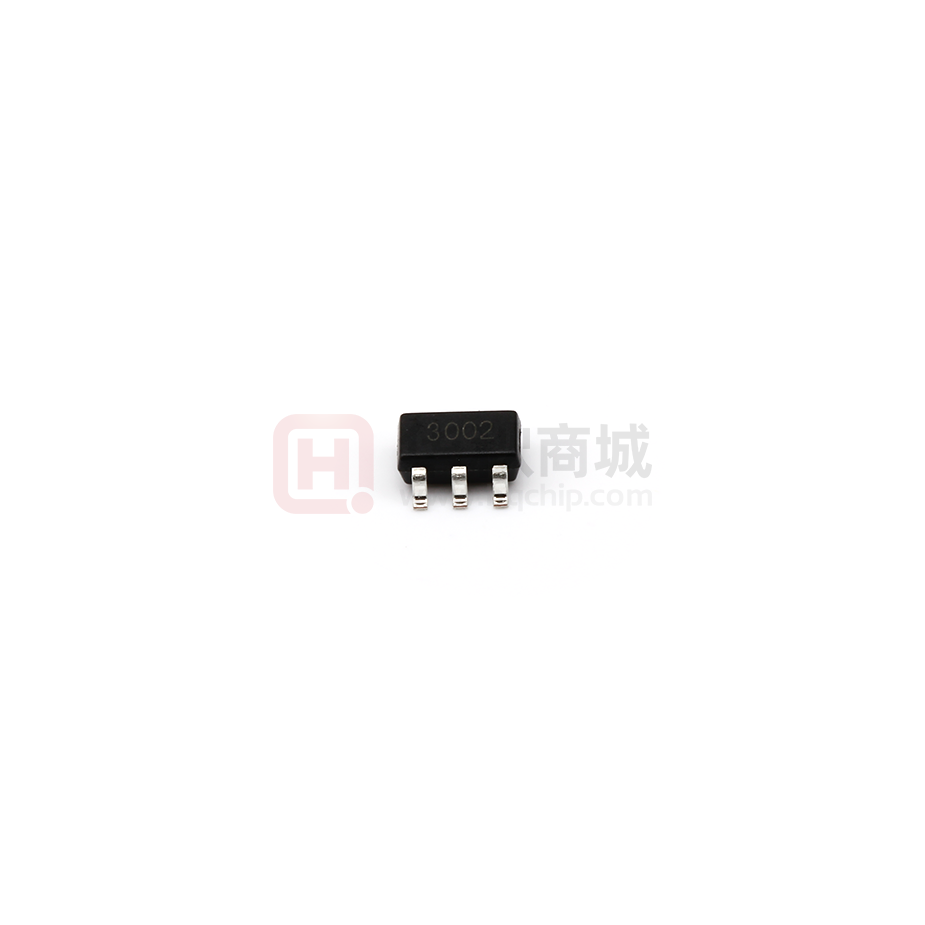
PJ3002SE
USB Charging Controller
Description
The PJ3002SE is the USB decated charging port controller IC. The IC is used to facilitate charging procedure when
most of the mainstream handheld devices are detected. The PJ3002SE is suitable for all the charger products using
USB interface like power bank, wall adapter and even MID device with OTG function. The IC is provided with enhanced
ESD protection up to +/-8kV with application on D+/D- Pins.
Features
⚫ Supports USB DCP Shorting D+ Line to D– Line per USB Battery Charging
Specification, Revision 1.2 (BC1.2)
⚫ Supports Shorted Mode (Shorting D+ Line to D-Line) per Chinese
Telecommunication Industry Standard YD/T 1591-2009
⚫ Supports USB DCP Applying 2.7 V on D+ Line and 2.7 V on D- Line
⚫ Supports USB DCP Applying 1.2 V on D+ and D– Lines
⚫ Automatically Switch D+ and D- Lines Connections for an Attached Device
⚫ Operating Range: 4.5 V to 5.5 V
⚫ Available in SOT-23-5 Package
Applications
Power bank
USB Ports (Hosts and Hubs)
Wall Charging Adapters
Block Diagram
www.pingjingsemi.com
Revision:2.0 Aug-2021
1/5
�PJ3002SE
USB Charging Controller
Pin Function And Descriptions
SOT-23-5
5.DM
1.NC
4.DP
2.GND
3.VCC
DESCRIPTION
Pin
NAME
1
NC
2
GND
Ground
3
VCC
Power
4
DP
USB positive data-channel to external USB device
5
DM
USB negative data-channel to external USB device
No Connected
Application Circuits
2.4A Configuration / Typical application circuits
www.pingjingsemi.com
Revision:2.0 Aug-2021
2/5
�PJ3002SE
USB Charging Controller
Absolute Maximum Ratings (at TA = 25°C)
Characteristics
Symbol
Rating
Unit
VIN to GND
-0.3 to +7
V
DP1,DM1,DP2,DM2 to GND
-0.3 to +6
V
Operating Junction Temperature
-40 to +125
°C
Storage Junction Temperature
-55 to +150
°C
Junction to Ambient Thermal Resistance
RθJA
180
°C/W
Junction to board thermal resistance
RθJB
120
°C/W
Junction to case thermal resistance
RθJC
42
°C/W
Value
Unit
±8000
V
ESD Ratings
Electrostatic discharge
Human-body model (HBM)
Recommended Operating Conditions
Symbol
Min.
Max.
Unit
Input voltage of VCC
VCC
4.5
5.5
V
DP1,DP2 data line input voltage
VDP
0
5.5
V
DM1,DM2 data line input voltage
VDM
0
5.5
V
DP1,DP2 Continuous sink or source current
IDP
0
±10
mA
DM1,DM2 Continuous sink or source current
IDM
0
±10
mA
www.pingjingsemi.com
Revision:2.0 Aug-2021
3/5
�PJ3002SE
USB Charging Controller
Electrical Characteristics
(TJ=25°C. VCC=5V, unless otherwise specified)
Characteristics
Symbol
Conditions
Min.
Typ.
Max.
Units
Input Voltage
VCC
4.3
5
5.5
V
UVLO Voltage
VUVLO
3.1
3.7
4.3
V
UVLO Hysteresis
Quiescent Current
ICCQ
VCC=5V
0.1
V
220
uA
BC 1.2 DCP Mode
DP,DM Short Resistance
Resistance between DPX
and GND
Resistance between DMX
and GND
DPx threshold of Goes to
divider mode
RDPM
160
200
Ω
RDPG
VDPx=0.8V
650
1000
KΩ
RDMG
VDMx=0.8V
650
1000
KΩ
VDPX_TH
300
mV
Divider Mode
DPx output voltage
VDPX_2.7
2.6
2.7
2.8
V
DMx output voltage
VDMX_2.7
2.6
2.7
2.8
V
DPx output impedance
RDPX
24
30
36
KΩ
DMx output impedance
RDMX
24
30
36
KΩ
DPX output voltgage
VDPX_1.2
1.12
1.2
1.28
V
DMX output voltgage
VDMX_1.2
1.12
1.2
1.28
V
1.2V /1.2V Mode
Note: 1. DPX Stands for DP1 or DP2, DMX Stands for DM1 or DM2
www.pingjingsemi.com
Revision:2.0 Aug-2021
4/5
�PJ3002SE
USB Charging Controller
Package Outline
SOT-23-5
Dimensions in mm
2.92
±0.1
0.127 +0.05/-0.02
1.9±0.1
1.6
2.8
±0.1
± 0.1
10
12
R0.15MAX
0.95 ±0.1
0.35±0.05
R0.15MAX
0.06
12
± 0.05
0.65
±0.1
1.1
±0.1
10
Ordering Information
Device
Package
Shipping
PJ3002SE
SOT-23-5
3,000PCS/Reel&7inches
www.pingjingsemi.com
Revision:2.0 Aug-2021
5/5
�
很抱歉,暂时无法提供与“PJ3002SE”相匹配的价格&库存,您可以联系我们找货
免费人工找货- 国内价格
- 5+0.35700
- 20+0.32550
- 100+0.29400
- 500+0.26250
- 1000+0.24780
- 2000+0.23730
- 国内价格
- 10+0.22810
- 100+0.22281
- 300+0.21935
