Si53360/61/62/65 Data Sheet
Low-Jitter, LVCMOS Fanout Clock Buffers with up to 12 outputs
and Frequency Range from dc to 200 MHz
The Si53360/61/62/65 family of LVCMOS fanout buffers is ideal for clock/data distribution and redundant clocking applications. The family utilizes Silicon Labs advanced
CMOS technology to fanout clocks from dc to 200 MHz with guaranteed low additive
jitter, low skew, and low propagation delay variability. Built-in LDOs deliver high PSRR
performance and eliminates the need for external components simplifying low jitter
clock distribution in noisy environments.
The CMOS buffers are available in multiple configurations with 8 outputs
(Si53360/61/65), or dual banks of 6 outputs each (Si53362). These buffers can be
paired with the Si534x clock generators and Si5xx oscillators to deliver end-to-end
clock tree performance.
KEY FEATURES
• Low additive jitter: 120 fs rms
• Built-in LDOs for high PSRR performance
• Up to 12 LVCMOS Outputs from LVCMOS
inputs
• Frequency range: dc to 200 MHz
• Multiple configuration options
• Dual Bank option
• 2:1 Input MUX option
• RoHS compliant, Pb-free
• Temperature range: –40 to +85 °C
VDD
Power Supply
Filtering
VDDO (Si53361 only)
OEA
8
CLK0
CLK1
Si53360/61
8 Outputs
VDD
VDDOA
Power Supply
Filtering
0
OEA
1
6
OE
6 Outputs
Si53362
CLK_SEL
6
CLK
8
8 Outputs
Si53365
6 Outputs
OEB
VDDOB
1
Skyworks Solutions, Inc. • Phone [781] 376-3000 • Fax [781] 376-3100 • sales@skyworksinc.com • www.skyworksinc.com
Rev. 1.3 • Skyworks Proprietary Information • Products and Product Information are Subject to Change Without Notice • July 26, 2021
1
�Table of Contents
1. Ordering Guide
. . . . . . . . . . . . . . . . . . . . . . . . . . . . . . 3
2. Functional Description. . . . . . . . . . . . . . . . . . . . . . . . . . . . 4
2.1 LVCMOS Input Termination .
.
.
.
.
.
.
.
.
.
.
.
.
.
.
.
.
.
.
.
.
.
.
.
.
. 4
2.2 Input Mux .
.
.
.
.
.
.
.
.
.
.
.
.
.
.
.
.
.
.
.
.
.
.
.
.
. 4
2.3 Output Clock Termination Options
.
.
.
.
.
.
.
.
.
.
.
.
.
.
.
.
.
.
.
.
.
.
. 5
2.4 AC Timing Waveforms
.
.
.
.
.
.
.
.
.
.
.
.
.
.
.
.
.
.
.
.
.
.
.
.
.
.
.
.
.
.
.
.
. 6
2.5 Power Supply Noise Rejection.
.
.
.
.
.
.
.
.
.
.
.
.
.
.
.
.
.
.
.
.
.
.
.
. 6
2.6 Typical Phase Noise Performance: Single-Ended Input Clock .
.
.
.
.
.
.
.
.
.
.
.
.
. 7
2.7 Input Mux Noise Isolation
.
.
.
.
.
.
.
.
.
.
.
.
. 8
.
.
.
.
.
.
.
.
.
.
.
.
.
3. Electrical Specifications . . . . . . . . . . . . . . . . . . . . . . . . . . . 9
4. Detailed Block Diagrams . . . . . . . . . . . . . . . . . . . . . . . . . .
12
5. Si5336x Pin Descriptions . . . . . . . . . . . . . . . . . . . . . . . . . .
15
5.1 Si53360 Pin Descriptions
.
.
.
.
.
.
.
.
.
.
.
.
.
.
.
.
.
.
.
.
.
.
.
.
.
.15
5.2 Si53361 Pin Descriptions
.
.
.
.
.
.
.
.
.
.
.
.
.
.
.
.
.
.
.
.
.
.
.
.
.
.17
5.3 Si53362 Pin Descriptions
.
.
.
.
.
.
.
.
.
.
.
.
.
.
.
.
.
.
.
.
.
.
.
.
.
.19
5.4 Si53365 Pin Descriptions
.
.
.
.
.
.
.
.
.
.
.
.
.
.
.
.
.
.
.
.
.
.
.
.
.
.21
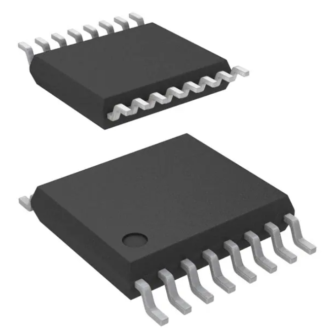
6. Package Outline . . . . . . . . . . . . . . . . . . . . . . . . . . . . .
22
6.1 16-Pin TSSOP Package .
.
.
.
.
.
.
.
.
.
.
.
.
.
.
.
.
.
.
.
.
.
.
.
.
.
.22
6.2 16-Pin QFN Package .
.
.
.
.
.
.
.
.
.
.
.
.
.
.
.
.
.
.
.
.
.
.
.
.
.
.
.24
6.3 24-Pin QFN Package .
.
.
.
.
.
.
.
.
.
.
.
.
.
.
.
.
.
.
.
.
.
.
.
.
.
.
.25
. . . . . . . . . . . . . . . . . . . . . . . . . . . .
26
7. PCB Land Pattern
7.1 16-Pin TSSOP Land Pattern .
.
.
.
.
.
.
.
.
.
.
.
.
.
.
.
.
.
.
.
.
.
.
.
.26
7.2 16-Pin QFN Land Pattern .
.
.
.
.
.
.
.
.
.
.
.
.
.
.
.
.
.
.
.
.
.
.
.
.
.27
7.3 24-Pin QFN Land Pattern .
.
.
.
.
.
.
.
.
.
.
.
.
.
.
.
.
.
.
.
.
.
.
.
.
.29
8. Top Markings . . . . . . . . . . . . . . . . . . . . . . . . . . . . . .
31
8.1 Si53360/65 Top Markings .
.
.
.
.
.
.
.
.
.
.
.
.
.
.
.
.
.
.
.
.
.
.
.
.
.31
8.2 Si53361 Top Marking .
.
.
.
.
.
.
.
.
.
.
.
.
.
.
.
.
.
.
.
.
.
.
.
.
.
.
.32
8.3 Si53362 Top Marking .
.
.
.
.
.
.
.
.
.
.
.
.
.
.
.
.
.
.
.
.
.
.
.
.
.
.
.33
9. Revision History . . . . . . . . . . . . . . . . . . . . . . . . . . . . .
34
2
Skyworks Solutions, Inc. • Phone [781] 376-3000 • Fax [781] 376-3100 • sales@skyworksinc.com • www.skyworksinc.com
Rev. 1.3 • Skyworks Proprietary Information • Products and Product Information are Subject to Change Without Notice • July 26, 2021
2
�Si53360/61/62/65 Data Sheet • Ordering Guide
1. Ordering Guide
Table 1.1. Si5336x Ordering Guide
3
Part Number
Input
LVCMOS Output
Output Enable
Frequency Range
Package
Si53360-B-GT
2:1 selectable MUX
LVCMOS
1 bank / 8 Outputs
Single
dc to 200 MHz
16-TSSOP
Si53361-B-GM
2:1 selectable MUX
LVCMOS
1 bank / 8 Outputs
(Settable VDDO)
Single
dc to 200 MHz
16-QFN
3x3 mm
Si53362-B-GM
2:1 selectable MUX
LVCMOS
2 banks / 6 Outputs
1 per bank
dc to 200 MHz
24-QFN
4x4 mm
SI53365-B-GT
1 bank / 1 Input
LVCMOS
1 bank / 8 Outputs
Single
dc to 200 MHz
16-TSSOP
Skyworks Solutions, Inc. • Phone [781] 376-3000 • Fax [781] 376-3100 • sales@skyworksinc.com • www.skyworksinc.com
Rev. 1.3 • Skyworks Proprietary Information • Products and Product Information are Subject to Change Without Notice • July 26, 2021
3
�Si53360/61/62/65 Data Sheet • Functional Description
2. Functional Description
The Si53360/61/62/65 are a family of low-jitter, low skew, fixed format (LVMCOS) buffers. These devices are available in multiple
configurations customized for the end application (refer to 1. Ordering Guide for more details on configurations).
2.1 LVCMOS Input Termination
The table below summarizes the various ac- and dc-coupling options supported by the LVCMOS device, and the figure shows the
recommended input clock termination.
Table 2.1. LVCMOS Input Clock Options
LVCMOS
AC-Coupled
DC-Coupled
1.8 V
No
Yes
2.5/3.3 V
Yes
Yes
VDD
VDD = 3.3 V, 2.5 V, or 1.8 V
CMOS
Driver
Si53360/61/62/65
Rs
CLKx
50
Note: Value for Rs should be chosen so that the total source impedance matches the characteristic impedance of the PCB trace.
Figure 2.1. Recommended Input Clock Termination
2.2 Input Mux
The Si53360-61/62 provide two clock inputs for applications that need to select between one of two clock sources. The CLK_SEL pin
selects the active clock input. The following table summarizes the input and output clock based on the input mux settings.
Table 2.2. Input Mux Logic
4
CLK_SEL
CLK0
CLK1
Q
L
L
X
L
L
H
X
H
H
X
L
L
H
X
H
H
Skyworks Solutions, Inc. • Phone [781] 376-3000 • Fax [781] 376-3100 • sales@skyworksinc.com • www.skyworksinc.com
Rev. 1.3 • Skyworks Proprietary Information • Products and Product Information are Subject to Change Without Notice • July 26, 2021
4
�Si53360/61/62/65 Data Sheet • Functional Description
2.3 Output Clock Termination Options
The recommended output clock termination options are shown below. Unused outputs should be left unconnected.
CMOS
Receivers
VDD
Si5336x
Zout
Rs
Zo
50
Note:
Rs = 33 ohm for 3.3 V and 2.5 V operation.
Rs = 0 ohm for 1.8 V operation.
Figure 2.2. LVCMOS Output Termination
5
Skyworks Solutions, Inc. • Phone [781] 376-3000 • Fax [781] 376-3100 • sales@skyworksinc.com • www.skyworksinc.com
Rev. 1.3 • Skyworks Proprietary Information • Products and Product Information are Subject to Change Without Notice • July 26, 2021
5
�Si53360/61/62/65 Data Sheet • Functional Description
2.4 AC Timing Waveforms
TPHL
CLK
TSK
QN
VPP/2
Q
VPP/2
QM
VPP/2
VPP/2
TPLH
TSK
Propagation Delay
Output-Output Skew
TF
Q
80% VPP
20% VPP
80% VPP
Q
20% VPP
TR
Rise/Fall Time
Figure 2.3. AC Timing Waveforms
2.5 Power Supply Noise Rejection
The device supports on-chip supply voltage regulation to reject power supply noise and simplify low-jitter operation in real-world environments. This feature enables robust operation alongside FPGAs, ASICs and SoCs and may reduce board-level filtering requirements.
See “AN491: Power Supply Rejection for Low-Jitter Clocks” for more information.
6
Skyworks Solutions, Inc. • Phone [781] 376-3000 • Fax [781] 376-3100 • sales@skyworksinc.com • www.skyworksinc.com
Rev. 1.3 • Skyworks Proprietary Information • Products and Product Information are Subject to Change Without Notice • July 26, 2021
6
�Si53360/61/62/65 Data Sheet • Functional Description
2.6 Typical Phase Noise Performance: Single-Ended Input Clock
Each of the phase noise plots superimposes Source Jitter and Total Jitter on the same diagram.
• Source Jitter - Reference clock phase noise (measured Single-ended to PNA).
• Total Jitter - Combined source and clock buffer phase noise measured as a single-ended output to the phase noise analyzer and
integrated from 12 kHz to 20 MHz. For more information, see 3. Electrical Specifications.
Note: To calculate the total RMS phase jitter when adding a buffer to your clock tree, use the root-sum-square (RSS).
Total jitter
measured here
AG E5052 Phase Noise
Analyzer
CLKx
CLK SYNTH
SMA103A
Si5336x
DUT
50
50 Ohm
Source jitter
measured here
Figure 2.4. Single-ended Measurement Method
The following figure shows three phase noise plots superimposed on the same diagram.
Frequency (MHz)
Single-Ended
Input Slew Rate (V/ns)
Source Jitter (fs)
Total Jitter
(SE) (fs)
Additive Jitter
(SE) (fs)
156.25
1.0
40.3
130.28
123.89
Figure 2.5. Total Jitter Single-Ended Input (156.25 MHz)
7
Skyworks Solutions, Inc. • Phone [781] 376-3000 • Fax [781] 376-3100 • sales@skyworksinc.com • www.skyworksinc.com
Rev. 1.3 • Skyworks Proprietary Information • Products and Product Information are Subject to Change Without Notice • July 26, 2021
7
�Si53360/61/62/65 Data Sheet • Functional Description
2.7 Input Mux Noise Isolation
The input clock mux is designed to minimize crosstalk between the CLK0 and CLK1. This improves phase jitter performance when
clocks are present at both the CLK0 and CLK1 inputs. The following figure shows a measurement of the input mux’s noise isolation.
Figure 2.6. Input Mux Noise Isolation (Single-ended Input Clock, 16QFN Package)
8
Skyworks Solutions, Inc. • Phone [781] 376-3000 • Fax [781] 376-3100 • sales@skyworksinc.com • www.skyworksinc.com
Rev. 1.3 • Skyworks Proprietary Information • Products and Product Information are Subject to Change Without Notice • July 26, 2021
8
�Si53360/61/62/65 Data Sheet • Electrical Specifications
3. Electrical Specifications
Table 3.1. Recommended Operating Conditions
Parameter
Symbol
Ambient Operating Temperature
TA
Test Condition
VDD
Supply Voltage Range
LVCMOS
Min
Typ
Max
Unit
–40
—
85
°C
1.71
1.8
1.89
V
2.38
2.5
2.63
V
2.97
3.3
3.63
V
Min
Typ
Max
Unit
Table 3.2. Input Clock Specifications
VDD = 1.8 V ± 5%, 2.5 V ± 5%, or 3.3 V ± 10%, TA = –40 to 85 °C
Parameter
Symbol
Test Condition
LVCMOS Input High Voltage
VIH
VDD x 0.7
—
—
V
LVCMOS Input Low Voltage
VIL
—
—
VDD x 0.3
V
Input Capacitance
CIN
—
5
—
pF
CLK0 and CLK1 pins with respect to GND
Table 3.3. DC Common Characteristics (CLK_SEL, OEx)
VDD = 1.8 V ± 5%, 2.5 V ± 5%, or 3.3 V ± 10%, TA = –40 to 85 °C
Parameter
Symbol
Core Supply Current
IDD1
Output Supply Current (per
clock output, Si53361/62 only)
IDDO1
Test Condition
Min
Typ
Max
Unit
VDD = 3.3 V, Si53360/65
—
150
—
mA
VDD = 3.3 V, Si53361/62
—
35
—
mA
VDDOX = 1.8 V
—
7
—
mA
VDDOX = 2.5 V
—
10
—
mA
VDDOX = 3.3 V
—
13
—
mA
Input High Voltage
VIH
VDD x 0.8
—
—
V
Input Low Voltage
VIL
—
—
VDD x 0.2
V
Internal Pull-up Resistor
RUP
—
25
—
kΩ
OEX, CLK_SEL
Note:
1. Frequency = 200 MHz, Cload = 0 pF
9
Skyworks Solutions, Inc. • Phone [781] 376-3000 • Fax [781] 376-3100 • sales@skyworksinc.com • www.skyworksinc.com
Rev. 1.3 • Skyworks Proprietary Information • Products and Product Information are Subject to Change Without Notice • July 26, 2021
9
�Si53360/61/62/65 Data Sheet • Electrical Specifications
Table 3.4. Output Characteristics (LVCMOS)
VDD = 1.8 V ± 5%, 2.5 V ± 5%, or 3.3 V ± 10%, TA = –40 to 85 °C
Parameter
Symbol
Test Condition
Min
Typ
Max
Unit
VDD x 0.8
—
—
V
—
—
VDD x 0.2
V
IOH = –12 mA, VDD = 3.3 V
Output Voltage High
VOH
IOH = –9 mA, VDD = 2.5 V
IOH = –6 mA, VDD = 1.8 V
IOL = 12 mA, VDD = 3.3 V
Output Voltage Low
VOL
IOL = 9 mA, VDD = 2.5 V
IOL = 6 mA, VDD = 1.8 V
Table 3.5. AC Characteristics
VDD = 1.8 V ± 5%, 2.5 V ± 5%, or 3.3 V ± 10%, TA = –40 to 85 °C
Parameter
Symbol
Test Condition
Min
Typ
Max
Unit
Frequency
F
LVCMOS
dc
—
200
MHz
DC
200 MHz, 2pF load TR/TF