PJM2310NSC
N-Channel Enhancement Mode Power MOSFET
Features
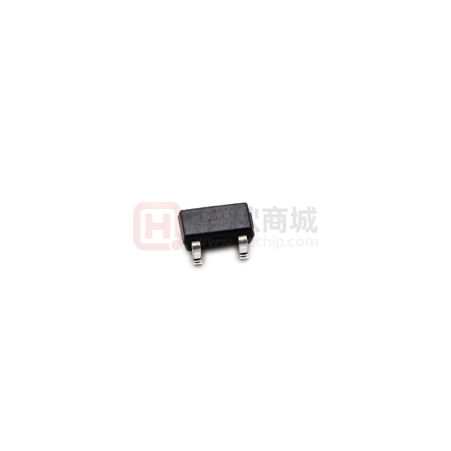
SOT-23-3
⚫ High power and current handing capability
⚫ VDS= 60V,ID= 3A
RDS(on)< 105mΩ @VGS= 10V
2
3
1
Application
1. Gate
2.Source
3.Drain
Marking Code:Q10
Battery switch
DC/DC converter
Schematic Diagram
3.Drain
1.Gate
2.Source
Absolute Maximum Ratings
Ratings at 25℃ ambient temperature unless otherwise specified.
Parameter
Symbol
Value
Unit
Drain-Source Voltage
VDS
60
V
Gate-Source Voltage
VGS
±20
V
Drain Current-Continuous
ID
3
A
Drain Current-Pulsed Note1
IDM
10
A
Maximum Power Dissipation
PD
1
W
Junction Temperature
TJ
150
°C
TSTG
-55 to +150
°C
RθJA
125
°C/W
Storage Temperature Range
Thermal Characteristics
Thermal Resistance,Junction-to-Ambient Note2
www.pingjingsemi.com
Revision:2.0 Aug-2021
1/7
�PJM2310NSC
N-Channel Enhancement Mode Power MOSFET
Electrical Characteristics
(Ta=25℃ unless otherwise specified)
Parameter
Symbol
Test Condition
Min.
Typ.
Max.
Unit
Drain-Source Breakdown Voltage
V(BR)DSS
VGS=0V,ID=250μA
60
--
--
V
Zero Gate Voltage Drain Current
IDSS
VDS=60V,VGS=0V
--
--
1
μA
Gate-Body Leakage Current
IGSS
VGS=±20V,VDS=0V
--
--
±100
nA
Gate Threshold Voltage Note3
VGS(th)
VDS=VGS,ID=250μA
1
1.35
2.5
V
Drain-Source On-Resistance Note3
RDS(on)
VGS=10V,ID=3A
--
78
105
mΩ
VGS=4.5V,ID=3A
--
96
125
mΩ
VDS=15V,ID=2A
--
3
--
S
--
510
--
pF
--
34
--
pF
Static Characteristics
Forward Transconductance Note3
gFS
Dynamic Characteristics
Input Capacitance
Ciss
Output Capacitance
Coss
Reverse Transfer Capacitance
Crss
--
26
--
pF
Turn-on Delay Time
td(on)
--
6
--
nS
Turn-on Rise Time
tr
VDD=30V, ID=3A
--
15
--
nS
Turn-off Delay Time
td(off)
VGS=10V,RGEN=1Ω
--
15
--
nS
VDS=30V,VGS=0V,f=1MHz
Switching Characteristics
Turn-off Fall Time
tf
--
10
--
nS
Total Gate Charge
Qg
--
14.6
--
nC
Gate-Source Charge
Qgs
--
1.6
--
nC
Gate-Drain Charge
Qgd
--
3
--
nC
--
--
1.2
V
--
--
3
A
VDS=30V,ID=3A,VGS=10V
Source-Drain Diode Characteristics
Diode Forward Voltage Note3
VSD
Diode Forward Current Note2
IS
VGS=0V,IS=3A
Note: 1. Repetitive Rating: Pulse width limited by maximum junction temperature.
2. Surface Mounted on FR4 Board, t ≤ 10 sec.
3. Pulse Test: Pulse width≤300μs, duty cycle≤2%.
www.pingjingsemi.com
Revision:2.0 Aug-2021
2/7
�PJM2310NSC
N-Channel Enhancement Mode Power MOSFET
ID Drain Current (A)
RDS(on) On-Resistance (Ω)
Typical Characteristic Curves
ID Drain Current (A)
ID Drain Current (A)
Normalized On-Resistance
VDS Drain-Source Voltage (V)
TJ Junction Temperature (℃)
C Capacitance (pF)
RDS(on) On-Resistance (Ω)
VGS Gate-Source Voltage (V)
VGS Gate-Source Voltage (V)
www.pingjingsemi.com
Revision:2.0 Aug-2021
VDS Drain-Source Voltage (V)
3/7
�VGS Gate-Source Voltage (V)
IS Reverse Drain Current (A)
PJM2310NSC
N-Channel Enhancement Mode Power MOSFET
VSD Source-Drain Voltage (V)
ID Drain Current (A)
Qg Gate Charge (nC)
r(t),Normalized Effective
Transient Thermal Impedance
VDS Drain-Source Voltage (V)
Square Wave Pluse Duration (sec)
www.pingjingsemi.com
Revision:2.0 Aug-2021
4/7
�PJM2310NSC
N-Channel Enhancement Mode Power MOSFET
Package Outline
SOT-23-3
Dimensions in mm
10
1.6
2.8
±0.1
0.127 +0.05/-0.02
±0.1
±0.1
2.92
12
R0.15MAX
0.95±0.1
0.35±0.05
R0.15MAX
0.06
12
± 0.05
0.65
±0.1
1.1
±0.1
10
Ordering Information
Device
Package
Shipping
PJM2310NSC
SOT-23-3
3,000PCS/Reel&7inches
www.pingjingsemi.com
Revision:2.0 Aug-2021
5/7
�PJM2310NSC
N-Channel Enhancement Mode Power MOSFET
Conditions of Soldering and Storage
Recommended condition of reflow soldering
Recommended peak temperature is over 245 OC. If peak temperature is below 245 OC, you may adjust
the following parameters:
Time length of peak temperature (longer)
Time length of soldering (longer)
Thickness of solder paste (thicker)
Conditions of hand soldering
Temperature: 370 OC
Time: 3s max.
Times: one time
Storage conditions
Temperature
5 to 40 OC
Humidity
30 to 80% RH
Recommended period
One year after manufacturing
www.pingjingsemi.com
Revision:2.0 Aug-2021
6/7
�PJM2310NSC
N-Channel Enhancement Mode Power MOSFET
Package Specifications
The method of packaging
Cover Tape
3,000 pcs per reel
SOT-23-3
Carrier Tape
30,000 pcs per box
10 reels per box
120,000 pcs per carton
4 boxes per carton
Embossed tape and reel data
D
A
T2
T1
Symbol
A
B
C
E
F
D
T1
T2
B
C
E
Value (unit: mm)
Ø 177.8±1
2.7±0.2
Ø 13.5±0.2
Ø 54.5±0.2
12.3±0.3
9.6+2/-0.3
1.0±0.2
1.2±0.2
F
Reel (7'')
www.pingjingsemi.com
Revision:2.0 Aug-2021
7/7
�
很抱歉,暂时无法提供与“PJM2310NSC”相匹配的价格&库存,您可以联系我们找货
免费人工找货- 国内价格
- 10+0.37120
- 100+0.29344
- 300+0.25456