RCLAMP0521P
ESD Protection Diode
RoHS Device
Halogen Free
Features
- Bi-directional ESD protection.
- IEC61000-4-2 Level 4 ESD protection.
- Working Voltage: 5V
- Typical capacitance: 0.3pF
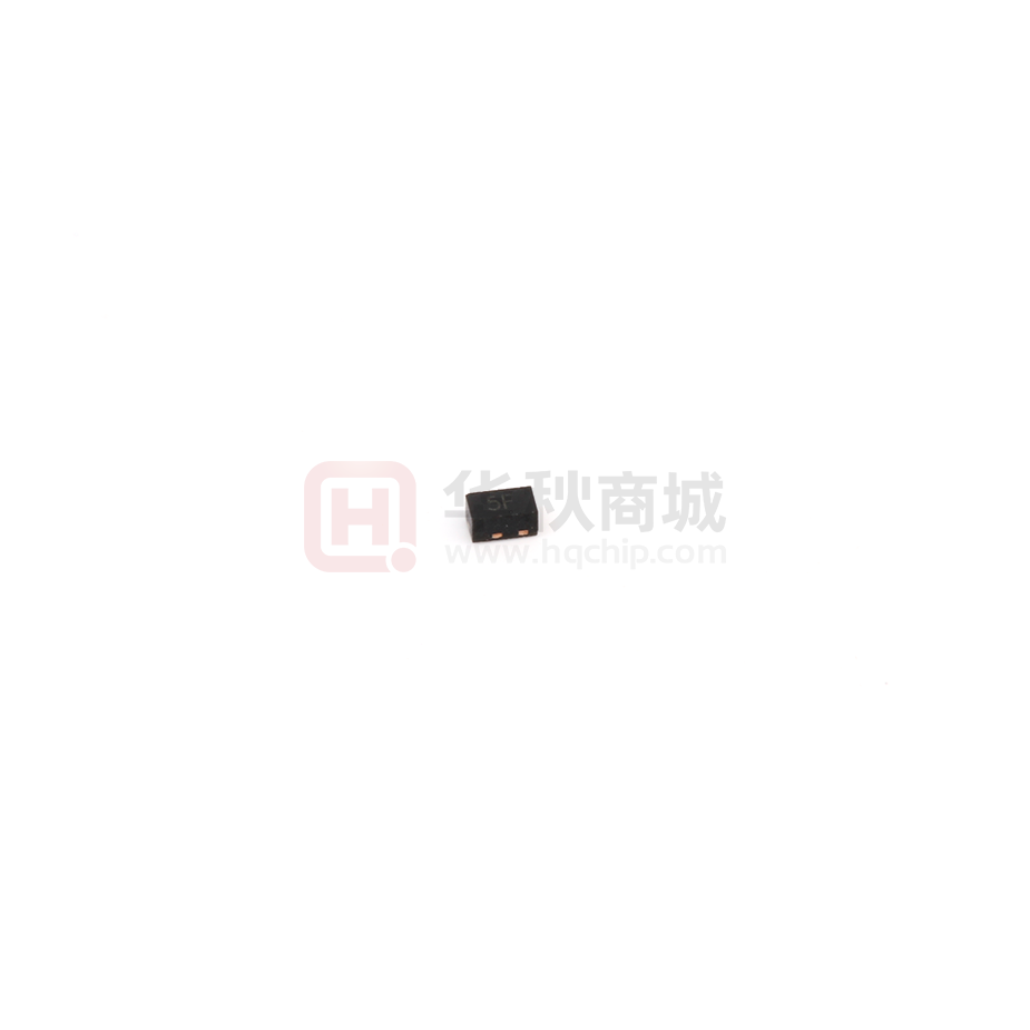
DNF1006-2L
0.041(1.05)
0.037(0.95)
0.026(0.65)
0.022(0.55)
Mechanical data
- Case: DFN1006-2L/0402 small outline plastic package.
molded plastic.
- Terminals: Gold plated, solderable per
MIL-STD-750, method 2026.
0.022(0.55)
0.018(0.45)
- Mounting position: Any.
0.001(0.02)
Max.
- High temperature soldering guaranteed:
260°C/10 second.
- Weight: 0.001 grams(approx.).
0.026(0.65)
BSC.
0.022(0.55)
0.018(0.45)
Circuit diagram
0.012(0.30)
0.008(0.20)
Dimensions in inches and (millimeter)
Maximum Rating ( at T =25°C unless otherwise noted )
A
Parameter
Peak pulse power ( tp = 8/20µs waveform)
ESD per IEC 61000-4-2(Air)
ESD per IEC 61000-4-2(Contact)
Symbol
Value
Unit
PPP
63
W
±15
±8
kV
TJ
-55 to +150
°C
TSTG
-55 to +150
°C
VESD
Operating temperature rang
Storage temperature rang
(1)
Electrical Characteristics ( at T =25°C unless otherwise noted )
A
Parameter
Conditions
Reverse stand-off voltage
Symbol
Min
Typ
Max
Unit
VRWM
-
-
5
V
Reverse leakage current
VR = 5 V
IR
-
-
100
nA
Reverse breakdown voltage
IR = 1 mA
V(BR)
6
-
10
V
VC
-
13
15
V
-
19
21
V
-
0.3
0.6
pF
IPP= 1 A
Clamping voltage
IPP= 3A
Junction capacitance
VC
VR= 0V , F=1MHz
(2)
CJ
Notes: 1. Device stressed with ten non-repetitive ESD pulses.
2. Non-Repetitive current pulse 8/20us exponential decay waveform according to IEC61000-4-5
1
�RCLAMP0521P
ESD Protection Diode
RATING AND CHARACTERISTIC CURVES (RCLAMP0521P)
Fig.1 - 8/20us Peak Pulse Current Wave
Form Acc. IEC 61000-4-5
Ta=25°C
Peak Valur Ipp
Percentage of Ipp
100%
0.60
Test Waveform
parameters
tf=8us
td=20us
Capacitance Between Terminals, (pF)
120%
Fig.2 - Typical Capacitance Between
Terminals Characteristics
e-t
80%
60%
40%
td= t Ipp/2
20%
0%
0.50
0.40
0.30
0.20
0.10
0
5
10
15
20
25
30
0
1
2
3
4
5
Time, (us)
Reverse Voltage, (V)
Fig.3 - Clamping Voltage Vs.
Peak Pulse Current
Fig.4 - Power Rating Derating Curve
30
Mounting on glass epoxy PCBs
100
Power Rating, (%)
Clamping voltage, (V)
25
20
15
10
Waveform
Parameters:
tr=8us
td=20us
5
80
60
40
20
0
0
1
2
0
3
25
50
75
100
125
Peak Pulse Current, (A)
Peak Pulse Current, (A)
2
150
�RCLAMP0521P
ESD Protection Diode
Reel Taping Specification
d
P0
P1
T
E
Index hole
F
W
B
P
C
A
12
o
0
D2
D1 D
W1
Trailer
Device
.......
.......
End
.......
.......
Leader
.......
.......
.......
.......
160mm (min)
Start
400mm (min)
Direction of Feed
DFN1006-2L
SYMBOL
A
B
C
d
D
D1
D2
(mm)
0.75 ± 0.05
1.17 ± 0.05
0.65 ± 0.05
1.50 + 0.10
- 0
178.00 ± 1.00
60.00 ± 0.50
13.50 ± 0.20
(inch)
0.030 ± 0.002
0.046 ± 0.002
0.026 ± 0.002
0.059 + 0.004
- 0
7.008 ± 0.039
2.362 ± 0.020
0.531 ± 0.008
SYMBOL
E
F
P
P0
P1
T
W
W1
(mm)
1.75 ± 0.10
3.50 ± 0.10
4.00 ± 0.10
4.00 ± 0.10
2.00 ± 0.10
0.20 + 0.02
- 0.05
8.00 ± 0.20
12.00 + 0.50
- 0
(inch)
0.069 ± 0.004
0.138 ± 0.004
0.157 ± 0.004
0.157 ± 0.004
0.079 ± 0.004
0.008 + 0.001
- 0.002
0.315 ± 0.008
0.472 + 0.020
- 0
DFN1006-2L
3
�RCLAMP0521P
ESD Protection Diode
Suggested PAD Layout
DFN1006-2L
SIZE
(mm)
(inch)
A
0.70
0.028
B
0.40
0.016
C
0.60
0.024
D
1.10
0.043
E
0.30
0.012
D
A
E
C
B
Standard Packaging
REEL PACK
Case Type
DFN1006-2L
REEL
Reel Size
( p cs )
(inch)
10,000
7
4
�
很抱歉,暂时无法提供与“RCLAMP0521P”相匹配的价格&库存,您可以联系我们找货
免费人工找货- 国内价格
- 10+0.16000
- 100+0.14950
- 500+0.13900
- 2000+0.12850
- 5000+0.12115
- 10000+0.11800