USBLC6-2SC6
ESD Protection Array
Description
Features
The usblc6-2sc6 is a low capacitance ESD Array,
utilizing leading monolithic silicon technology to
provide fast response time and low ESD clamping
voltage, making this device an ideal solution for
protecting voltage sensitive high-speed data lines.
The usblc6-2sc6 has an ultra low capacitance with a
typical value at 0.4pF, and complies with the IEC
61000-4-2 (ESD) standard with ±30kV air and
±25kV contact discharge. It is assembled into a
6-pin lead-free SOT23-6 package. The low
capacitance array make it ideal for four high speed
data and transmission line. This device is optimized
for ESD protection of portable electronics.
Mechanical Characteristics
Applications
Package: SOT23-6
Lead Finish: Matte Tin
UL Flammability Classification Rating 94V-0
Case Material: “Green” Molding Compound
Moisture Sensitivity: Level 3 per J-STD-020
Terminal Connections: See Diagram Below
Marking Information: See Below
Dimensions and Pin Configuration
I/O 1
VCC
6
5
Ultra low capacitance: 0.4pF typical (I/O to I/O)
Ultra low leakage: nA level
Low operating voltage: 5V
Low clamping voltage
2 data lines and one power line protects
Complies with following standards:
– IEC 61000-4-2 (ESD) immunity test
Air discharge: ±30kV
Contact discharge: ±25kV
– IEC61000-4-4 (EFT) 40A (5/50ns)
– IEC61000-4-5 (Lightning) : 5A(8/20μs)
ROHS Compliant
USB 2.0 Ports
Digital video interface(DVI)
Monitor and Flat Panel Displays
Gigabit Ethernet
Marking Information
I/O 2
4
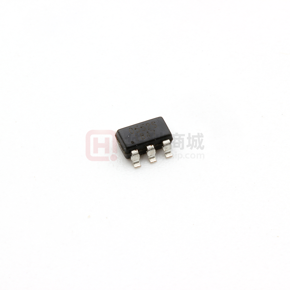
0552S
YYWW
1
2
3
I/O 1
GND
I/O 2
0552S = Device Marking Code
YYWW=Date Code
Dot denotes Pin1
Circuit and Pin Schematic
1/4
�USBLC6-2SC6
ESD Protection Array
Absolute Maximum Ratings (TA=25°C unless otherwise specified)
Parameter
Symbol
Value
Unit
Peak Pulse Power(tp=8/20μs)
PPP
100
W
Peak Pulse Current(tp=8/20μs)
IPP
5
A
ESD per IEC 61000−4−2 (Air)
±30
VESD
ESD per IEC 61000−4−2 (Contact)
Operating Temperature Range
Storage Temperature Range
±25
kV
TJ
−55 to +125
°C
Tstg
−55 to +150
°C
Electrical Characteristics (TA=25°C unless otherwise specified)
Parameter
Reverse Working Voltage
Breakdown Voltage
Symbol
Min
Typ
VRWM
VBR
Max
Unit
5
V
6
Test Condition
V
IT = 1mA
Reverse Leakage Current
IR
0.5
µA
VRWM = 5V
Clamping Voltage
VC
10
V
IPP = 1A (8 x 20µs pulse)
Clamping Voltage
VC
20
V
IPP = 5A (8 x 20µs pulse)
Junction Capacitance
CJ
0.6
0.8
pF
VR = 0V, f = 1MHz, any I/O pin to
ground
Junction Capacitance
CJ
0.3
0.4
pF
VR = 0V, f = 1MHz, between I/O pins
2/4
�USBLC6-2SC6
ESD Protection Array
10
2.0
Peak Pulse Power_Ppp (W)
Juncxtion Capacitance_Cj (pF)
Typical Performance Characteristics (TA=25℃ unless otherwise Specified)
1.6
1.2
0.8
0.4
0.0
1
0.1
0.01
0
1
2
3
4
5
0.1
10
100
1000
Pulse Duration_tp (us)
Peak Pulse Power vs. Pulse Time
50
120
40
100
% of Rated Power
Clamping Voltage_Vc (V)
Reverse Voltage_VR (V)
Junction Capacitance vs. Reverse Voltage
1
30
20
10
80
60
40
20
0
0
2
4
6
8
Peak Pulse Current_Ipp (A)
0
10
0
25
50
75
100 125
Ambient Temperature_Ta(℃)
Power Derating Curve
Clamping Voltage vs. Peak Pulse Current
8 X 20μs Pulse Waveform
ESD Clamping Voltage
8 kV Contact per IEC61000−4−2
3/4
150
�USBLC6-2SC6
ESD Protection Array
SOT23-6 Package Outline Drawing
SYM
A
A1
A2
b
c
D
E1
E
e
e1
N
aaa
ccc
DIMENSIONS
MILLIMETERS
MIN
NOM
MAX
MIN
0.90
1.45
0.035
0.00
0.15
0.000
0.90
1.15
1.30
0.035
0.25
0.50
0.010
0.08
0.22
0.003
2.80
2.90
3.10
0.110
1.50
1.60
1.75
0.060
2.80 BSC
0.95 BSC
1.90 BSC
6
0.10
0.20
INCHES
NOM
0.045
0.114
0.063
0.110 BSC
0.037 BSC
0.075 BSC
6
0.004
0.008
Suggested Land Pattern
DIMENSIONS
MILLIMETERS
2.50
1.40
0.95
0.60
1.10
3.60
SYM
C
G
P
X
Y
Z
4/4
INCHES
0.098
0.055
0.037
0.024
0.043
0.141
MAX
0.057
0.006
0.051
0.020
0.009
0.122
0.069
�
很抱歉,暂时无法提供与“USBLC6-2SC6”相匹配的价格&库存,您可以联系我们找货
免费人工找货