PJ1117SQ
Low Dropout Regulators
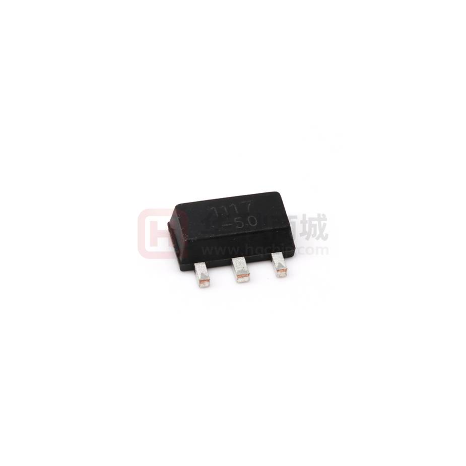
SOT-89
Description
PJ1117SQ is a low-dropout three-terminal Linear regulator circuit with positive
2.VOUT
voltage output. It is divided into two versions, Fixed voltage output version and
Adjustable voltage output version:The fixed output voltage is
1.2V、1.8V、2.5V、3.3V、5V and the adjustable version can provide the
output voltage from 1.25V to 5V with only 2 external resistors.
1.GND/ADJ 2.VOUT
3.VIN
Features
⚫ Range of operation input voltage : Max.15V
⚫ Current limiting function
⚫ Thermal Shutdown
⚫ Operation Ambient Temperature : -40~85°C
Applications
⚫ LCD Monitor and LCD TV
⚫ DVD Decode Boar
⚫ ADSL Modem
Functional Pin Description
Pin Name
GND/ADJ
VOUT
VIN
Pin Function
Ground/Adjustable Pin
Output Voltage
Power Input Voltage
Marking Code
1117
-XX
XX:Output Voltage
e.g. 18:1.8V 33:3.3V
www.pingjingsemi.com
Revision:4.0 Nov-2021
1/7
�PJ1117SQ
Low Dropout Regulators
Ordering Information
PJ1117SQ-
Output Voltage
12 : 1.2V 18 : 1.8V 25 : 2.5V
33 : 3.3V 50 : 5.0V
Package Type
SQ : SOT-89
Function Block Diagram
www.pingjingsemi.com
Revision:4.0 Nov-2021
2/7
�PJ1117SQ
Low Dropout Regulators
Absolute Maximum Ratings
Ratings at 25℃ ambient temperature unless otherwise specified.
Parameter
Symbol
Rating
Unit
Supply Voltage
VIN
18
V
Junction Temperature
TJ
150
°C
Storage Temperature
TSTG
-40 to +150
°C
Thermal Resistance Junction-to-Ambient
RθJA
45
°C/W
Note: These are stress ratings only. Stresses exceeding the range specified under Absolute Maximum Ratings may cause
substantial damage to the device. Functional operation of this device at other conditions beyond those listed in the specification is
not implied and prolonged exposure to extreme conditions may affect device reliability.
Recommended Operating Conditions
Parameter
Symbol
Rating
Unit
Recommended Maximum Input Voltage
VIN
15
V
Recommended Operating Junction Temperature
Topr
-40 to +85
°C
www.pingjingsemi.com
Revision:4.0 Nov-2021
3/7
�PJ1117SQ
Low Dropout Regulators
Fixed Voltage Output Version
Electrical Characteristics
(TA=25℃ , unless otherwise noted.)
Parameter
Symbol
Test Conditions
Min.
Typ.
Max.
Unit
Output Voltage Accuracy
∆VOUT
0≤IOUT≤1A,VIN=VOUT+2V
-2
--
+2
%
--
2
5
mA
--
2
5
mA
IOUT=100mA
--
1.15
1.3
V
IOUT=1A
--
1.3
1.5
V
--
0.03
0.2
VOUT=1.2V
Quiescent Current
IQ
IOUT=0mA, VIN=10V
1.8V≤VOUT≤5V
IOUT=0mA, VIN=12V
Dropout Voltage
VDROP
VOUT=1.2V
Line Regulation
∆VLINE
IOUT=10mA, 2.7V≤VIN≤10V
1.8V≤VOUT≤5V
IOUT=10mA, VOUT+1.5V≤VIN≤12V
Load Regulation
∆VLOAD
Temperature coefficien
∆V/∆T
10mA≤IOUT≤1A,
VIN=VOUT+1.5V
%/V
--
0.03
0.2
--
--
36
mV
--
+100
--
ppm
Adjustable Voltage Output Version
Electrical Characteristics
(TA=25℃ , unless otherwise noted.)
Parameter
Symbol
Test Conditions
Min.
Typ.
Max.
Unit
Vref
10mA≤IOUT≤1A , VIN=3.25V
1.225
1.25
1.275
V
Line Regulation
∆VLINE
IOUT=10mA, 2.75V≤VIN≤12V
--
0.03
0.2
%/V
Load Regulation
∆VLOAD
10mA≤IOUT≤1A,VIN=2.75V
--
2
8
mV
--
2
10
mA
Reference voltage
Minimum load current
Imin
Adjust pin current
Iadj
10mA≤IOUT≤1A, VIN=5V
--
55
120
μA
Ichange
10mA≤IOUT≤1A, VIN=5V
--
0.2
10
μA
Iadj change
www.pingjingsemi.com
Revision:4.0 Nov-2021
4/7
�PJ1117SQ
Low Dropout Regulators
Typical Application Circuit
PJ1117SQ has an adjustable version and six fixed versions (1.2V, 1.8V, 2.5V, 3.3V and 5V)
Fixed Voltage Output Version
PJ1117SQ
C1:10uF
C2:10uF
1. Recommend using 10uF tan capacitor as bypass capacitor (C1) for all application circuit.
2. Recommend using 10uF tan capacitor to assure circuit stability.
Adjustable Voltage Output Version
PJ1117SQ
C1:10uF
C2:10uF
The output voltage of adjustable version follows the equation: VOUT=1.25×(1+R2/R1)+IAdj×R2. We can ignore IAdj
because IAdj (about 50uA) is much less than the current of R1 (about 2~10mA).
(1). To meet the minimum load current (>10mA) requirement, R1 is recommended to be 125ohm or lower. As
PJ1117SQ-ADJ can keep itself stable at load current about 2mA, R1 is not allowed to be higher than 625Ω.
(2). Using a bypass capacitor (CADJ) between the ADJ pin and ground can improve ripple rejection. This bypass
capacitor prevents ripple from being amplified as the output voltage is increased. The impedance of CADJ should be
less than R1 to prevent ripple from being amplified. As R1 is normally in the range of 100Ω~500Ω, the value of CADJ
should satisfy this equation: 1/(2π×fripple×CADJ)
很抱歉,暂时无法提供与“PJ1117SQ-5.0”相匹配的价格&库存,您可以联系我们找货
免费人工找货- 国内价格
- 5+0.35237
- 20+0.32072
- 100+0.28907
- 500+0.25742
- 1000+0.24265
- 2000+0.23210
- 国内价格
- 5+0.56916
- 50+0.44993
- 150+0.39032