Ap
pplicatiions Noote: SY
Y7701
H
High
Effi
ficiency 500kHz,
5
25V PW
WM Contrroller
For WLED backligh
ht application
Generral Descrription
Feeatures
SY7701 is a current moode boost conntroller targetedd for
d
has a wide
WLED backlight appliication. The device
input volltage range of
o 3V to 255V. The external
compensaation provides flexible adjuustment of coontrol
loop for different appllications. The internal low side
driver is capable of sourcing
s
1.5A
A and sinkingg 3A
current.
Orderring Infoormation
n
SY7701 □(□□)□
Temperature Coode
T
P
Package
Code
O
Optional
Spec Code
C
Orderingg Number
SY7701DBC
SY77701FHC
Package type
DFN3x3-10
SOP10
•
•
•
•
Input
I
voltage range
r
3V to 255V
500kHz fixed switching freqquency
d
frequuency
100Hz~1kHz dimming
10%~100% dimming duty cyycle @200Hz dimming
frequency
f
• External
E
comppensation
• Integrated
I
low
w side driver: 1.5A sourcing and
a 3A
sinking
• OVP,
O
OTP funnctions
• RoHS
R
Compliant and Halogeen Free
• Compact
C
packkage: DFN3x3--10,SOP10
Ap
pplicatioons
Note
----
• Monitor
M
LCD Panel Backligght
• TV
T LCD Paneel Backlight
• LED
L
Lighting
Typiccal Applications
SY7701
Figure 1. Schematic Diagram
SY77011 Rev. 0.2A
Silergyy Corp. Connfidential- Prrepared for Internal
I
Usee Only
1
SY7
7701
Pinou
ut (top vieew)
(DF
FN3x3-10)
(SOP10)
Top
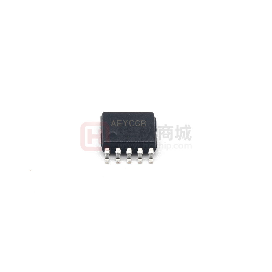
p Mark: GOxyyz for SY7701DBC (Device code:GO, x=yyear code, y=w
week code, z= loot number cod
de)
AEYxxyz for SY7701FHC (Devicee code:AEY, x=year
x
code, y=
=week code, z=
= lot number code)
c
Pin Nam
me
Pinn Number
Pin Desccription
IN
10
Input pin. Decouple
D
this pin
p to GND pinn with at least 1uF ceramic capacitor
5V Internall LDO output from
f
VIN. Connnect a 4.7 uF ccapacitor from
m this pin
VCC
C
9
to GND
GATE
E
8
Driver pin. Connect to thee gate of power MOSFET
Current sennse pin. Connecct an external current
c
sensingg resistor RS frrom this
pin to GND
D. The voltage on this pin is used
u
to providee mosfet curren
nt
CS
7
feedback inn the control loop and cycle by
b cycle peak ccurrent limit. Peak
P
current limiit is triggered when
w
the senseed voltage pluss the slope
compensation exceed 340
0mV
Feedback pin. The LED current
c
equals to:
t
ILED= 100mmV
FB
6
RISEET
GND
D
5(Expposed Paddle)
COMP
4
OVP
P
3
SS
2
EN/PW
WM
1
Ground pinn
External compensation pin. Connect RC
C network from
m this pin to GN
ND to
oop
compensatee the control lo
Over Voltagge Protection input
i
pin.The OVP
O
set point equals to :
VOVP=
1
ROV22
(R
OV!
+R
OV2
)
Soft start piin. Connect a capacitor
c
from this pin to GN
ND to program the soft
start time
Enable and PWM dimmin
ng input pin. Puull it high to tuurn on the chip
p. Do not
float this pin
Absolu
ute Maxim
mum Ratin
ngs (Note 1)
IN,EN -------------------------------------------------------------------------------------------------------------------------------------------V
GATE------------------------------------------------------------------------------------------------------------------------------ VC
CC+0.3V
All other pins
p --------------------------------------------------------------------------------------------------------------------------------- V
Power Disssipation, PD @ TA = 25°C, DFN3x3-10,SOP10 ------------------------------------------------------------ 2.6W/TBD
Package Thermal
T
Resisttance (Note 2)
θJA ---------------------------------------------------------------------------------------------------------------------------------------------------------------------- 38°C
C/W/TBD
θJC -------------------------------------------------------------------------------------------------------------------------------------------------------------------- 130°C
C/W/TBD
Junction Temperature
T
R
Range
-------------------------------------------------------------------------------------------------------- 125°C
Lead Tem
mperature (Solddering, 10 sec.) ------------------------------------------------------------------------------------------- 260°C
Storage Temperature
T
Raange ---------------------------------------------------------------------------------------------- 65°C to 150°C
Recom
mmended Operating
O
g Conditioons (Note 3)
IN ------------------------------------------------------------------------------------------------------------------------------------- V to 25V
Junction Temperature
T
R
Range
--------------------------------------------------------------------------------------------- 40°C to 125°C
Ambient Temperature
T
R
Range
--------------------------------------------------------------------------------------------- 40°C
C to 85°C
SY77011 Rev. 0.2A
Silergyy Corp. Connfidential- Prrepared for Internal
I
Usee Only
2
SY7701
Electrical Characteristics
(VIN = 12V, TA = 25°C, unless otherwise specified)
Parameter
Input Voltage Range
Quiescent Current
Shutdown Current
OVP Threshold
FB Input Current
Feedback Reference Voltage
Internal Slope Compensation
Gate Driver Output Peak Current
EN Rising Threshold
EN Falling Threshold
Input UVLO threshold
UVLO hysteresis
Oscillator Frequency
Min On Time
Min Off Time
Internal LDO Output
Thermal Shutdown
Thermal Hysteresis
Symbol
VIN
IQ
ISHDN
VOVP
IFB
VREF
VSLOPE
ISOURCE
ISINK
VENH
VENL
VUVLO
VHYS
FOSC
VVCC
TSD
THYST
Conditions
Min
3
VOVP=1.1V
EN=0
0.98
-50
98
Typ
170
0.1
1
100
40
1.5
3
Max
25
1.02
50
102
1.5
0.4
2.9
VIN=5.5V
4.9
0.3
500
200
200
5
150
20
5.1
Unit
V
uA
uA
V
nA
mV
mV/uS
A
A
V
V
V
V
kHz
ns
ns
V
℃
℃
Note 1: Stresses beyond the “Absolute Maximum Ratings” may cause permanent damage to the device. These are
stress ratings only. Functional operation of the device at these or any other conditions beyond those indicated in the
operational sections of the specification is not implied. Exposure to absolute maximum rating conditions for
extended periods may affect device reliability.
Note 2: θ JA is measured in the natural convection at TA = 25°C on a low effective single layer thermal conductivity
test board of JEDEC 51-3 thermal measurement standard.Test condition: Device mounted on 2” x 2” FR-4 substrate
PCB, 2oz copper, with minimum recommended pad on top layer and thermal vias to bottom layer ground plane.
Note 3: The device is not guaranteed to function outside its operating conditions.
SY7701 Rev. 0.2A
Silergy Corp. Confidential- Prepared for Internal Use Only
3
SY7701
Block Diagram
COMP
CS
IN
5V
LDO
1V
FB
VCC
Slope
Comp
100mV
Control
Logic
Driver
GATE
ISEN
Soft-start
Thermal
Protection
GND
SY7701 Rev. 0.2A
SS
EN
Silergy Corp. Confidential- Prepared for Internal Use Only
4
SY7701
Typical Performance Characteristics
SY7701 Rev. 0.2A
Silergy Corp. Confidential- Prepared for Internal Use Only
5
SY7701
SY7701 Rev. 0.2A
Silergy Corp. Confidential- Prepared for Internal Use Only
6
SY7701
Operation
SY7701 is a boost controller targetted for white LED
lighting. It integrates a low side driver which is capable
of sourcing 1.5A and sinking 3A current. External
compensation can supply a flexible adjustment of
control loop under different applications. OVP function
can protect the part from LED open event, OVP point
can be programmed using a voltage divider.
Inductor L:
There are several considerations in choosing this
inductor.
1) Choose the inductance to provide the desired
ripple current. It is suggested to choose the ripple
current to be about 40% of the maximum average input
current. The inductance is calculated as:
L=
Applications Information
LED current programming resister RISET
LED current is programmed by a resistor which is in
series with the LED string. LED current is calculated as:
ILED=100mV/Riset
LED may be shorted if the current is higher than its
rating. SY7701 will fold back the LED current from 100%
to 30% when the OVP pin voltage changes from 0.5V to
0.15V. For typical application, it is recommended the
OVP point is less than twice of the LED string voltage
OVP point programming divider ROV1 and ROV2:
Choose proper resistor ROV1 and ROV2 to program the
output voltage OVP point. VOVP is calculated as:
VOVP=1V*(1+ROV1/ROV2)
Make sure the resister will not exceed its power rating
when output voltage reaches the OVP point.
Peak Current Sense Resistor
An external sensing resistor Rsen is used to sense the
current flow through the MOSFET. The sensed voltage
is for peak current mode control and cycle by cycle
peak current limit. Peak current limit will be triggered
when the voltage on CS pin plus the internal slop
compensation exceed 340mV, which is the typical
clamping voltage of the PWM comparator. It is
desirable to make the maximum value of sensing
voltage plus the slope compensation to be about 70%
of the clamping voltage during normal operation. Thus,
Rs=
70% × 0.34-Vslope× D× Ts
IPEAK
Vslope is the slew rate of the internal compensation,
IPEAK is the peak current through MOSFET.
.
SY7701 Rev. 0.2A
⎛ VIN ⎞2
(VOUT − VIN)
⎟
⎜
⎝ VOUT ⎠ FSW × IOUT, MAX × 40%
where FSW is the switching frequency and IOUT,MAX is
the maximum load current.
The SY7701 regulator IC is quite tolerant of different
ripple current amplitude. Consequently, the final choice
of inductance can be slightly off the calculation value
without significantly impacting the performance.
2)
The saturation current rating of the inductor must
be selected to be greater than the peak inductor
current under full load conditions.
ISAT,MIN >
3)
⎛ VOUT ⎞
× IOUT_MAX + VIN(VOUT − VIN)
⎜ V ⎟IN
2 × FSW × L× VOUT
⎝
⎠
The DCR of the inductor and the core loss at the
switching frequency must be low enough to
achieve the desired efficiency requirement. It is
desirable to choose an inductor
with
DCR