Datasheet – epc901
CCD line sensor 1024x1 pixel
General Description
Features
The epc901 is a high-performance CCD line sensor capable of
storing a total of 4 frames in the frame store elements for ultra
high-speed image acquisition. The acquisition of the image is controlled by a control signal SHUTTER. The epc901 flags when a
frame is ready for read-out by asserting the DATA_RDY signal.
The transmission of the frame over the video amplifier is controlled
by the external control signal READ. When a read-out is initiated
by a pulse on the READ signal, it is sampled by a CDS stage. After
a fixed delay the frame can be shifted out through the video amplifier by applying the appropriate amount of read clock edges.
■ Photosensitive CCD array backside illuminated with 1024x1 pixel
■ Very high frame rate
■ Very high sensitivity due to 100% fill factor and ESPROS' unique
OHC15L process technology
■ Pixel size 7.5 x 120μm
■ On-chip correlated-double sampling
■ Single-ended or differential analog output
■ Simple 5-pin control interface for acquisition and read-out
■ I2C bus interface
■ Internal clock source, trimmable
■ Two on-chip temperature sensors
■ Single supply voltage
■ 32 Pin space saving CSP package
■ Chip size L x W x T: 8.0 x 1.3 x 0.23 mm
The device offers various configuration options:
■ Gain of the read-out stage selectable of 1, 2 or 4
■ Transmission direction left to right and right to left
■ Region of interest (ROI) center region (pixel 256 to 767)
■ Binning of 2 or 4 pixels to reduce transmission time and noise
■ Single- or multi-frame acquisition
■ Clearing of frames stored and periodic flushing of pixel array to
avoid blooming
Applications
■ Linear and rotary encoder
■ Triangulation light barrier / distance measurement
■ Line sensor / camera
■ Business card readers & portable scanners
■ Multi-touch displays / electronic white boards
■ Finger print readers
■ Spectrometers
■ Check & ticket readers
■ Speed measurement
■ Bar code readers
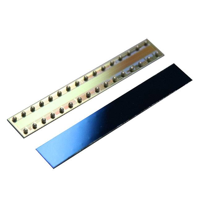
Figure 1: Backside illuminated CMOS/CCD imager
CCD 1024x1
Configuration
Inputs
Logic
Frame store 1
Frame store 2
Frame store 3
Frame store 4
Configuration
I2C-bus
I2C-Interface
1024 : 1 MUX
Analog output
Figure 2: Block diagram
© 2020 ESPROS Photonics Corporation
Characteristics subject to change without notice
1 / 32
Datasheet_epc901-V7.00
www.espros.com
�Table of Contents
1. Block diagram.....................................................................................................................................................3
2. Pin-out................................................................................................................................................................3
2.1. Power domains....................................................................................................................................................................................5
3. Electrical, optical and timing characteristics............................................................................................................6
3.1. Electrical and other characteristics......................................................................................................................................................6
3.2. Temperature sensor characteristics....................................................................................................................................................7
3.3. Timing parameters...............................................................................................................................................................................7
3.4. Absolute maximum ratings..................................................................................................................................................................8
3.5. Optical characteristics..........................................................................................................................................................................9
3.6. Frequency response..........................................................................................................................................................................10
3.7. Video amplifier frequency response..................................................................................................................................................10
4. Configuration.................................................................................................................................................... 11
5. Imager operation................................................................................................................................................12
5.1. General remarks................................................................................................................................................................................12
5.2. Single frame acquisition.....................................................................................................................................................................12
5.3. Multi frame acquisition.......................................................................................................................................................................13
5.4. Image readout....................................................................................................................................................................................13
5.5. ROI / binning read clock....................................................................................................................................................................14
5.6. Flush..................................................................................................................................................................................................14
6. Various features.................................................................................................................................................15
6.1. Temperature sensor..........................................................................................................................................................................15
6.2. Power-down.......................................................................................................................................................................................15
6.3. Oscillator clock trimming....................................................................................................................................................................15
6.4. Reset..................................................................................................................................................................................................15
7. I2C interface......................................................................................................................................................16
7.1. I2C communication............................................................................................................................................................................16
7.1.1. Device addressing..........................................................................................................................................................................16
7.1.2. Single-byte write.............................................................................................................................................................................16
7.1.3. Multi-byte write................................................................................................................................................................................16
7.1.4. Single-byte read..............................................................................................................................................................................17
7.1.5. Multi-byte read................................................................................................................................................................................17
7.1.6. Software reset.................................................................................................................................................................................17
7.1.7. Device address sampling...............................................................................................................................................................17
7.1.8. Setup latency..................................................................................................................................................................................17
7.2. I2C bus timing....................................................................................................................................................................................18
8. Register description...........................................................................................................................................19
8.1. Binning, amplifier gain, ROI, read direction.......................................................................................................................................19
8.2. Video Amplifier bandwidth.................................................................................................................................................................20
8.3. Video amplifier bandwidth, noise and current consumption..............................................................................................................20
8.4. Configuration control, video amplifier on/off......................................................................................................................................20
8.5. Video amplifier SE/Diff, charge pump on/off, 5V regulator on/off.....................................................................................................21
8.6. Oscillator trimming (fine)....................................................................................................................................................................21
8.7. Oscillator trimming (coarse)...............................................................................................................................................................22
8.8. Temperature sensors read................................................................................................................................................................22
8.8.1. Left temperature sensor.................................................................................................................................................................22
8.8.2. Right temperature sensor...............................................................................................................................................................22
8.9. Temperature sensors control.............................................................................................................................................................23
8.10. I2C error flag....................................................................................................................................................................................23
8.11. Chip revision....................................................................................................................................................................................23
9. Application information......................................................................................................................................24
9.1. Differential mode................................................................................................................................................................................24
9.2. Single ended mode............................................................................................................................................................................25
9.3. External components.........................................................................................................................................................................25
9.4. Low noise operation...........................................................................................................................................................................25
9.4.1. Charge pump noise........................................................................................................................................................................25
9.4.2. Video amplifier noise......................................................................................................................................................................25
9.4.3. Layout recommendations...............................................................................................................................................................26
10. Power consumption considerations....................................................................................................................27
10.1. General considerations....................................................................................................................................................................27
10.2. Low power operation.......................................................................................................................................................................27
11. Layout and packaging information......................................................................................................................28
11.1. Mechanical dimensions...................................................................................................................................................................28
11.2. PCB design and SMD manufacturing process considerations.......................................................................................................29
11.3. Tape & Reel Information..................................................................................................................................................................29
11.4. Soldering and IC handling...............................................................................................................................................................29
12. Self-test mode by fill-and-spill............................................................................................................................30
13. Ordering Information........................................................................................................................................31
14. IMPORTANT NOTICE........................................................................................................................................32
© 2020 ESPROS Photonics Corporation
Characteristics subject to change without notice
2 / 32
Datasheet_epc901-V7.00
www.espros.com
�1. Block diagram
CCD
Control
CCD pixel field 1024 x 1
FS4
FS3
FS2
FS1
CCD frame store buffer FS1..4
Floating diffusion / source follower / CDS
Shift
Control
1024:4 multiplexer
4:1 multiplexer
VDD_OA
analog in
VIDEO_P
VIDEO_CM
VIDEO_N
AMP
CLR_DATA
digital control
SHUTTER
READ
GND_OA
DATA_RDY
Control
ROI_SEL
VDD
Charge pump
RD_DIR
HOR_BIN
VDD_7V0
AGND
Oscillator
I2C Interface
CS0
TEST_MODE
ANA_TEST_0
PWR_DOWN
I_BIAS
GAIN
BW0
BW1
DGND
Temperature
Sensor
1&2
Test
Control
AMP
Control
Power supply /
Power on
Reset
ANA_TEST_1
AGND
SCL
1.8V regulator
CS1
5V regulator
VDD_1V8
SDA
VDD_5V0
Figure 3: Block diagram
2. Pin-out
32
31
30
29
28
27
26
25
24
23
22
21
20
19
18
17
11
12
13
14
15
16
epc901
1
2
3
4
5
6
7
8
9
10
Figure 4: Pin-out, view to the photo-sensitive side (top-view)
© 2020 ESPROS Photonics Corporation
Characteristics subject to change without notice
3 / 32
Datasheet_epc901-V7.00
www.espros.com
�Pin no. Pin name
Digital pins
2
PWR_DOWN
3
CLR_DATA
5
CLR_PIX
6
SHUTTER
12
READ
4
DATA_RDY
13
SDA
14
SCL
15
ROI_SEL
17
CS1
19
CS0
21
GAIN
22
BW0
23
BW1
24
RD_DIR
25
HOR_BIN
30
TEST_MODE
Analog pins
8
VIDEO_N
9
VIDEO_P
11
VIDEO_CM
27
I_BIAS
28
ANA_TEST_1
29
ANA_TEST_0
Supply pins
26
VDD
10
VDD_OA
32
VDD_1V8
18
VDD_5V0
20
VDD_7V0
16
AGND
1
AGND
7
GND_OA
31
DGND
Pin type
DI
DI
DI
DI
DI
Default [V] Description
0
0
0
0
0
DO
DIOD
DIOD
DI
TER
TER
TER
TER
TER
DI
TER
DI
AO
AO
AI
AI
AIO
AIO
Supply
Supply
AO / Supply
Supply
Supply
Supply
Supply
VDD
VDD
0
VDD/2
VDD/2
VDD/2
VDD/2
VDD/2
0
VDD/2
0
Power-down mode enable
Clear internal data memory controller
Rising edge resets pixels and its controller
Exposure active when SHUTTER set
Read-out control and read clock
Flag when data on video interface is ready. Used as a strap pin to turn on/off
the charge pump
I2C serial data (open drain)
I2C serial clock (open drain)
Region of interest selection
I2C chip select 1
I2C chip select 0
Select gain of read-out path
LSB of bandwidth of video amplifier
MSB of bandwidth of video amplifier
Read-out direction
Horizontal binning selection
Chip test
Negative terminal of video output
Positive terminal of video output
VDD/2 or 0 Voltage to set video output common-mode
Bias current
0
Analog test in-/output 1
0
Analog test in-/output 0, rising edge indicates the last pixel in a frame
Positive chip supply voltage
Positive supply of video amplifier
Decoupling
Decoupling / external 5V supply for low power consumption (refer to 10.2.)
Decoupling
Analog ground
Analog ground
Video amplifier ground
Digital ground
Definitions:
■ DI:
■ DO:
■ DIOD:
■ AO:
■ AI:
■ AIO:
■ TER:
Digital input pin, with an internal pull-down resistor of approx. 100-250kΩ
Digital output pin
General purpose bidirectional digital pin with open-drain output, requires external pull-up resistor
Analog output
Analog input
Analog input and output
Ternary input pin, with a pull-down and an equal pull-up resistor of approx. 100-250kΩ which tie the pin to the VDD/2 state.
© 2020 ESPROS Photonics Corporation
Characteristics subject to change without notice
4 / 32
Datasheet_epc901-V7.00
www.espros.com
�2.1. Power domains
VDD
VDD_5V0
VDD_7V0
VDD_OA
VDD_1V8
The epc901 chip has internally 5 different power domains and 3 ground references which are interconnected with ESD protection diodes.
All pins are also equipped with ESD protection diodes. Figure 5 shows this functional circuit. The diodes have a breakthrough voltage of
0.3V. The designer has to take care that none of these diodes become conductive either at power-up, power-down or normal operation.
epc 901
VIDEO_P
VIDEO_N
VIDEO_CM
I_BIAS
ANA_TEST_0
ANA_TEST_1
analog pins
DGND
all others
TEST_MODE
GND_OA
digital pins
AGND
GND_OA
DGND
AGND
Figure 5: ESD protection diode circuit
© 2020 ESPROS Photonics Corporation
Characteristics subject to change without notice
5 / 32
Datasheet_epc901-V7.00
www.espros.com
�3. Electrical, optical and timing characteristics
(TA = 25°C, VDD = 3.0V unless otherwise noted)
3.1. Electrical and other characteristics
Parameter
Description
Min
Typ
Max
Unit
VDD Nominal
Nominal supply voltage on VDD and VDD_OA
2.70
3.00
3.45
V
Supply voltage on VDD and VDD_OA
with Read Clock of max. 1 MHz.
2.45
PSRR
Power supply rejection ratio VDD and VDD_OA.
Differential
13
dB
IDD+IDD_OA 1
Total current consumption on pins VDD and VDD_OA
(refer to section 10.)
Single ended
9
dB
Differential mode,
full video bandwidth, 46kfps 2,
Charge pump:
ON
Temperature sensors:
ON
Idle mode (READ = L)
26
39
mA
Peak, during read-out
48
72
mA
Differential mode,
full video bandwidth, 46kfps 2,
external VDD5V0 supply 3
Charge pump:
OFF
Temperature sensors:
OFF
Idle mode (READ = L)
10
15
mA
Peak, during read-out
16
24
mA
Differential mode,
low video bandwidth, 1kfps 4,
external VDD5V0 supply 3
Charge pump:
OFF
Temperature sensors:
OFF
Idle mode (READ = L)
6.0
9.0
mA
Peak, during read-out
6.0
9.0
mA
Single-ended mode,
low video bandwidth, 1kfps 4
Charge pump:
ON
Temperature sensors:
ON
Idle mode (READ = L)
21
30
mA
Peak, during read-out
40
60
mA
Single-ended mode,
low video bandwidth, 1kfps 4,
external VDD5V0 supply 3
Charge pump:
OFF
Temperature sensors:
OFF
Idle mode (READ = L)
5.0
10.0
mA
Peak during read-out
5.0
10.0
mA
Power-Save mode (POWR_DOWN = H, shutter still working),
external VDD5V0 supply 3
Charge pump:
OFF
Temperature sensors:
OFF
1.3
2
mA
In-rush current at power-up during approximately 5ms
Charge pump:
ON
60
90
mA
In-rush current at power-up during approximately 2ms,
external VDD5V0 supply 3
Charge pump:
OFF
50
75
mA
1.2
2.5
mA
0.2*VDD
V
IDD_5V
Current consumption on pin VDD_5V0 3,
Differential/single-ended mode, full video bandwidth, 46kfps
external VDD5V0 supply 3)
Charge pump:
OFF
VDIL
Low voltage level on binary digital inputs 5 (Level L)
VDIH
High voltage level on binary digital inputs (Level H)
VDOL, VTERIL
Low voltage level on binary and ternary digital outputs (Level L)
VDOH, VTERIH
High voltage level on binary and ternary digital outputs (Level H)
0.8*VDD
VTERIM
Centre voltage level on ternary digital inputs (Level M)
0.4*VDD
IDI
Sink current at digital inputs
RDI
Internal pull-down resistor
RTER
Internal voltage dividing resistors which force the input to VDD/2
IDO
Sink / source current at digital outputs
VVDD1V8
Internally generated voltage on pin VDD1V8
1.62
1.8
VVDD5V0
Internally generated voltage on pin VDD5V0
4.5
5.0
5.5
V
VVDD7V0
Internally generated voltage on pin VDD7V0
6.0
6.5
7.0
V
VVIDEO_P,N
Voltage range at output of video amplifier (@ gain 1)
0.25
VDD-0.25
V
VCM_SE
Voltage at VIDEO_CM to select single-ended mode
0.4
V
2
5
© 2020 ESPROS Photonics Corporation
Characteristics subject to change without notice
6 / 32
0.5*VDD
V
0.2*VDD
V
V
0.6*VDD
V
10
μA
100
250
kΩ
100
250
kΩ
3
mA
1.98
V
Datasheet_epc901-V7.00
www.espros.com
�Parameter
Description
Min
Typ
Max
Unit
VCM_D
Common-mode voltage in differential mode, set on pin
VIDEO_CM. Note: For VCM_D>1V, differential mode is detected automatically by default. For VCM_D Frame Store Buffers --> CDS
VIDEO_CM
GND_OA
I_BIAS
7
27
DGND
31
AGND
16
1
AGND
VIDEO_N
RBIAS
9
ADC
11
8
Pins 8 and 11:
Can be left not
connected.
Refer to the note
below.
Figure 16: Single ended mode application diagram
If VIDEO_N and VIDEO_CM are tied to GND at power-up or RESET, single-ended mode is enabled. The output signal is available at
VIDEO_P.
Note:
If the pins VIDEO_N and VIDEO_CM are not connected, the epc901 is in differential mode after power-up or RESET. In this case, singleended mode can be selected via I2C register setting FORCE_ANA_CTRL_SIGS, bit AMP_OVR (see Table 14 and Table 15).
Illumination
VIDEO_P (typ.)
Dark voltage
0.4V
Maximum video output
2.0V
Table 28: Video amplifier output in single-ended mode
9.3. External components
The external components in Figure 15 and Figure 16 shall be as follows:
Parameter
Description
Value
Units
Tolerance Comments
RBIAS
Bias resistor
56k
kΩ
±1%
Temperature coefficient max. ±100ppm/K
CVDD1V8
Decoupling capacitor
1.0
μF
±20%
low ESR
CVDD5V0, CVDD7V0 Decoupling capacitors
2.2
μF
±20%
low ESR
CVDD, CVDD_OA
Decoupling capacitors
1.0
μF
±20%
low ESR
L
Decoupling inductor
600
Ω
@100MHz, e.g. Taiyo Yuden BK1005HR601-T
9.4. Low noise operation
9.4.1. Charge pump noise
The internal charge pump generates some noise, especially in single-ended mode. The noise performance can be optimized by turning off
the charge pump and supplying the chip with an external 5V supply. Refer to section 10.2.
9.4.2. Video amplifier noise
Another noise source is the video amplifier which can be used in two different modes. Single ended mode is the lower noise operation
mode. Thus, use the chip in single ended mode for low noise applications. In addition, operate the video amplifier at lowest possible band width and lowest current consumption. Refer to 8.2. and 8.3.
© 2020 ESPROS Photonics Corporation
Characteristics subject to change without notice
25 / 32
Datasheet_epc901-V7.00
www.espros.com
�9.4.3. Layout recommendations
The epc901 line imager is a very high sensitivity analog/digital chip. Due to its high conversion gain, just a few electrons collected by
coupling to signal lines close to the chip generate a significant voltage at the output. Thus, do not place any signal lines underneath the
chip without shielding. It is highly recommended to place a stable AGND plane underneath the epc901 chip (on the top layer of the PCB)
and not to place any signal tracks close to the chip.
Also very important is a clean noise-free power supply. Especially decouple the VDD from VDD_OA with capacitor so the output modula tion of the video amplifier does not modulate the VDD of the chip. Make sure all the capacitors used for decoupling are low ESR types.
The READ signal line can also be a major source of noise or coupling to the output signal. Figure 17 shows a scope screen shot of such a
coupling problem.
VIDEO_P
READ
Figure 17: READ signal coupling to the output by a ground loop
The source of such problems is usually a ground loop. Especially if there is a significant distance 'd' as shown in Figure 18 (starting from a
few cm only) between the video output of the epc901 chip and the input of the ADC. Care has to be taken that the layout of the GND lines
is exactly like shown in Figure 18. Make sure that the digital GND has a separate track as shown by the blue ground line!
d
VDD
VDD_OA
VDD_5V0
VIDEO_P
31
1
GND_OA
epc 901
VDD_7V0
GNDD
20
VDD_1V8
GNDA
18
GNDA
32
12
READ
10
VDD
26
16
VIDEO_N
VDD
9
ADC
8
AGND
7
GND
Common AGND
connection
Digital
control
Common GND
connection
READ
DGND
Figure 18: Recommended ground and power supply connections
Make also sure that the thick lines in Figure 18 are as short and as thick as possible.
© 2020 ESPROS Photonics Corporation
Characteristics subject to change without notice
26 / 32
Datasheet_epc901-V7.00
www.espros.com
�10. Power consumption considerations
10.1. General considerations
There are several options to control the power consumption. However, a trade-off between performance and power consumption has to be
considered. The following section describes the various options. The most power-consuming blocks are
•
Temperature sensors (approx. 3mA)
•
Video amplifier (approx. 3.5mA)
•
Charge pump and 5V regulator (approx. 13.5mA)
The wake-up time of the video amp is typ. 3µs only. Thus, in most applications it can be turned off during illumination in order to reduce the
average power consumption.
10.2. Low power operation
The lowest possible power consumption of the epc901 can be achieved if it is supplied with 3V and 5V since the highest power consumption is the internal charge pump which generates the 5V from VDD. In this case, the chip-internal charge pump and the internal 5V regu lator shall be turned off. The power consumption in this configuration is less than 20mW compared to 80mW in the standard mode. The
following application information shows how this can be achieved. Follow carefully the instructions in order to avoid damage of the chip.
Use protection diodes according to circuit diagram below. The diodes have to be low voltage Schottky devices with a forward current of at
least 100mA (i.e. BAT74).
IN_+3.0V
Ext. supply
+3.0V
VDD
26
epc 901
D1
VDD_OA
DGND
VDD_7V0
31
GND_OA
20
D2
10
VDD_5V0
AGND
18
D3
AGND
Ext. supply
+5.0V
IN_+5.0V
32
VDD_1V8
1
16
7
GND
Common GND
connection
Common AGN
connection
Make sure that external 5V supply (VDD_5V0) is delayed by at least 100µs to the VDD.
1. Power up VDD (3V)
2.
3.
Wait for at least 100µs
Power up VDD_5V0
VDD
VDD_5V0
>100µs
Figure 19: Power up sequence in low power configuration
© 2020 ESPROS Photonics Corporation
Characteristics subject to change without notice
27 / 32
Datasheet_epc901-V7.00
www.espros.com
�11. Layout and packaging information
11.1. Mechanical dimensions
(0.050)
The packaging technology is a CSP with a uBGA. All measures which do not have an explicit tolerance are meant +/-0.001mm.
Photosensitive side
(top view)
Solder balls Sn96.5Ag3.0Cu0.5
(SAC305)
0.190 ±0.020
PCB side
8.080 ±0.040
4.080 ±0.020
1024 x 0.0075 = 7.680
0.0075
photosensitive area
center of pixel-field
17
0.618
Pixel #1023
top view (view to photosensitive side)
(ball size: 0.200)
(0.232 ±0.020)
1
(0.330 ±0.020)
0.860
Pixel #0
0.850 ±0.020
1.324 ±0.040
0.120
32
16
0.090
0.500
3.750
15 x 0.500 = 7.500
Weight: 4.57 mg
- dimensions in mm
- not specified tolerances ±0.001
The photosensitive area is not marked neither on the front nor on the backside of the IC. As a visible reference, the metal ring of the IC can
be used which is visible from the back side (solder ball side). Also from the front side (photosensitive area) it can be seen with a camera
which is sensitive in the near infrared wavelength domain (950 .. 1150nm).
Figure 20 shows the epc901 chip from the bottom side with view to the solder balls. Please note the location of pin 1.
Pin 1
Figure 20: Bottom view
© 2020 ESPROS Photonics Corporation
Characteristics subject to change without notice
28 / 32
Datasheet_epc901-V7.00
www.espros.com
�11.2. PCB design and SMD manufacturing process considerations
The epc901 chip comes in a very small 32 pin chip scale package, the PCB layout should be made with special care. The silicon chip is
small and light weight compared to its solder balls. It is highly recommended that all tracks to the chip should come straight from the side.
A consequent symmetrical PCB layout design is highly recommended to achieve high production yield.
The pads and the tracks should also have exactly the same width. The tracks shall be covered by a solder resist mask in order to avoid
drain of the solder tin alloy to the track.
solder resist mask opening
solder resist mask
1.324
ø0.3
min. 0.25
solder paste resist coverage
8.000
track
(straight only for 0.25mm!)
landing pad
max. 0.15
ø0.4
chip perimeter
all measures in mm
Figure 21: Recommended PCB layout
Underfill of the components reduces stress to the solder pads caused by e.g. temperature cycling or mechanical bending. The thermal and
mechanical fatigue will be reduced and the longterm reliability will be increased. Underfill and underfill selection is application specific. It
shall follow JEDEC-STD JEP150: Stress-Test-Driven Qualification of and Failure Mechanisms Associated with Assembled Solid State
Surface- Mount Components.
Please refer to the application note AN08_Process-Rules_CSP_Assembly. Please follow carefully the recommendations in this application
note to achieve a high manufacturing yield.
11.3. Tape & Reel Information
The devices are packed in tape on reel for automatic placement systems. The tape is wound on 178 mm (7 inch) or 330 mm (13 inch)
reels and individually packaged for shipment. General tape-and-reel specification data are available in a separate data sheet and indicate
the tape sizes for various package types. Further tape-and-reel specifications can be found in the Electronic Industries Association (EIA)
standard 481-1, 481-2, 481-3.
CSP32 Tape
12
Pin 1
4
ESPROS does not guaranteeCSP6
that there
Thus, the pick-and-place
machine should check the presence of a chip dur Tape are no empty cavities.
QFN16 Tape
Pin 1
Pin 1
ing picking.
8
11.4. Soldering and IC handling
12
Since the chip is only 50μm thick and has a high aspect ratio (length to width), a careful handling during the surface mount assembly
process shall be taken in order to avoid mechanical damage. In addition to that, careful PCB layout is needed in order to achieve reliable
assembly results with a high yield. Please refer to the application note AN08_Process-Rules_CSP_Assembly which contains most up to
date and comprehensive information to these topics. This application note can be downloaded at www.espros.com/application-notes.
4
8
© 2020 ESPROS Photonics Corporation
Characteristics subject to change without notice
29 / 32
Datasheet_epc901-V7.00
www.espros.com
�12. Self-test mode by fill-and-spill
The CCD and the readout chain functionality of the epc901 chip can be tested without optical stimulation. This function is useful in a factory test of the final product or in safety applications. The concept is to inject electrically stimulated charge into the pixel instead of photon
generated charge by the as-called fill-and-spill circuitry.
The basic behavior of the IC by the fill-and-spill circuitry is exactly the same as when the IC is illuminated. I.e. also when fill-and-spill is
used, the acquisition is controlled by SHUTTER, the internal flush and shift operation are similar and the signal DATA_RDY is asserted at
the end of the internal shift operation.
If the CCD is stimulated by the fill-and-spill, the on-chip test controller coordinates the operation of the fill-and-spill and the CCD.
Fill-and-spill procedure:
1. Select differential readout mode.
2. Apply the following voltages:
TEST_MODE = VDD
ROI_SEL = 0V or VDD
RD_DIR = 0V or VDD
3. Access the test mode configuration registers. Write access remains available until next reset:
Addr 0xD0: 0x4A
Addr 0xD1: 0x66
Addr 0xD2: 0x02
Addr 0xD4: 0x20
Addr 0xD5: 0x21
4. Select the pattern of pixels to be stimulated by writing to register Addr 0xD3 (see Table 29):
Bit select
Stimulation
7
not used
6
all odd pixels
5
pixels 2, 6, 10 etc.
4
pixels 4, 12, 20 etc.
3
pixels 0, 8, 16 etc.
2:0
Set these bits to 0x1
Table 29: Bit select description of register Addr 0xD3 in fill-and-spill test mode
5. Apply the following voltages to the test pins. Note that Vout varies from production lot to lot:
ANA_TEST_0 = 1 VDC
ANA_TEST_1 (VIDEO_P – VIDEO_N):
◦
◦
3.0 VDC for Vout of approx. -0.3V
3.6 VDC for Vout of approx. +0.5V
6. Wait 10 µs
7. Acquire a frame by using a 20µs SHUTTER signal. A different integration time is not allowed.
8. Read the frame as described in section 5.4.
9. Disconnect external voltage sources from pins ANA_TEST_0/1.
10. Configure test mode registers to their initial values:
Addr 0xD4: 0x00
Addr 0xD5: 0x01
Addr 0xD2: 0x00
Addr 0xD3: 0x00
11. Apply the following voltages:
TEST_MODE = 0V
ROI_SEL → application dependent
RD_DIR → application dependent
Important notes:
■ The chip does not operate correctly if the procedure and the write sequences described above are not exactly executed.
■ ANA_TEST* are bi-directional pins, by default output pins. Thus, the voltages V IN and VDC may only be applied once the chip is in fill-andspill mode. Otherwise, it can get damaged!
© 2020 ESPROS Photonics Corporation
Characteristics subject to change without notice
30 / 32
Datasheet_epc901-V7.00
www.espros.com
�13. Ordering Information
Part Number
Part Name
Package
RoHS
Packaging
Method
P100 401
epc901-CSP32-033
CSP32
Yes
Reel
P100 208
epc901 Evaluation Board V2
PCB 70.00 x 65.00 mm
Yes
Anti static bag
P100 209
epc901 Chip Carrier Board V2
PCB 36.00 x 42.75 mm
Yes
Anti static bag
Table 30: Ordering information
Application notes can be downloaded from the ESPROS website at www.espros.com/downloads/09_Application_notes.
© 2020 ESPROS Photonics Corporation
Characteristics subject to change without notice
31 / 32
Datasheet_epc901-V7.00
www.espros.com
�14. IMPORTANT NOTICE
ESPROS Photonics AG and its subsidiaries (ESPROS) reserve the right to make corrections, modifications, enhancements, improvements, and other changes to its products and services at any time and to discontinue any product or service without notice. Customers
should obtain the latest relevant information before placing orders and should verify that such information is current and complete. All products are sold subject to ESPROS’ terms and conditions of sale supplied at the time of order acknowledgment.
ESPROS warrants performance of its hardware products to the specifications applicable at the time of sale in accordance with epc’s stan dard warranty. Testing and other quality control techniques are used to the extent ESPROS deems necessary to support this warranty. Except where mandated by government requirements, testing of all parameters of each product is not necessarily performed.
ESPROS assumes no liability for applications assistance or customer product design. Customers are responsible for their products and
applications using ESPROS components. To minimize the risks associated with customer products and applications, customers should
provide adequate design and operating safeguards.
ESPROS does not warrant or represent that any license, either express or implied, is granted under any ESPROS patent right, copyright,
mask work right, or other ESPROS intellectual property right relating to any combination, machine, or process in which ESPROS products
or services are used. Information published by ESPROS regarding third-party products or services does not constitute a license from ESPROS to use such products or services or a warranty or endorsement thereof. Use of such information may require a license from a third
party under the patents or other intellectual property of the third party, or a license from ESPROS under the patents or other intellectual
property of ESPROS.
Resale of ESPROS products or services with statements different from or beyond the parameters stated by ESPROS for that product or
service voids all express and any implied warranties for the associated ESPROS product or service. ESPROS is not responsible or liable
for any such statements.
ESPROS products are not authorized for use in safety-critical applications (such as life support) where a failure of the ESPROS product
would reasonably be expected to cause severe personal injury or death, unless officers of the parties have executed an agreement specifically governing such use. Buyers represent that they have all necessary expertise in the safety and regulatory ramifications of their appli cations, and acknowledge and agree that they are solely responsible for all legal, regulatory and safety-related requirements concerning
their products and any use of ESPROS products in such safety-critical applications, notwithstanding any applications-related information or
support that may be provided by epc. Further, Buyers must fully indemnify ESPROS and its representatives against any damages arising
out of the use of ESPROS products in such safety-critical applications.
ESPROS products are neither designed nor intended for use in military/aerospace applications or environments unless the ESPROS prod ucts are specifically designated by ESPROS as military-grade. Only products designated by ESPROS as military-grade meet military spec ifications. Buyers acknowledge and agree that any such use of ESPROS products which ESPROS has not designated as military-grade is
solely at the Buyer's risk, and that they are solely responsible for compliance with all legal and regulatory requirements in connection with
such use.
ESPROS products are neither designed nor intended for use in automotive applications or environments unless the specific ESPROS
products are designated by ESPROS as compliant with ISO/TS 16949 requirements. Buyers acknowledge and agree that, if they use any
non-designated products in automotive applications, ESPROS will not be responsible for any failure to meet such requirements.
© 2020 ESPROS Photonics Corporation
Characteristics subject to change without notice
32 / 32
Datasheet_epc901-V7.00
www.espros.com
�