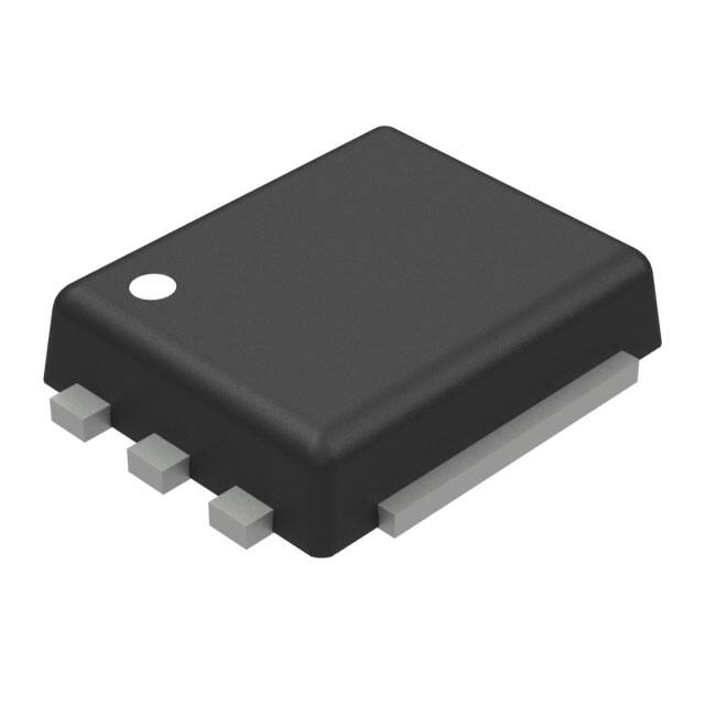
S-57RB S Series
www.ablic.com
AUTOMOTIVE, 150°C OPERATION,
HIGH-WITHSTAND VOLTAGE, HIGH-SPEED,
BIPOLAR HALL EFFECT LATCH IC
Rev.1.4_00
© ABLIC Inc., 2019-2021
This IC, developed by CMOS technology, is a high-accuracy Hall effect latch IC that operates with high temperature and
high-withstand voltage.
The output voltage level changes when this IC detects the intensity level of magnetic flux density and a polarity change.
Using this IC with a magnet makes it possible to detect the rotation status in various devices.
ABLIC Inc. offers a "magnetic simulation service" that provides the ideal combination of magnets and our Hall effect ICs
for customer systems. Our magnetic simulation service will reduce prototype production, development period and
development costs. In addition, it will contribute to optimization of parts to realize high cost performance.
For more information regarding our magnetic simulation service, contact our sales representatives.
ABLIC Inc. offers FIT rate calculated based on actual customer usage conditions in order to support customer functional
safety design.
For more information regarding our FIT rate calculation, contact our sales representatives.
Caution
This product can be used in vehicle equipment and in-vehicle equipment. Before using the product for
these purposes, it is imperative to contact our sales representatives.
Features
• Uses a thin (t0.80 mm max.) TSOT-23-3S or ultra-thin (t0.50 mm max.) HSNT-6(2025) package, allowing for device
miniaturization
• Contributes to reduction of mechanism operation dispersion with high-accuracy magnetic characteristics
(Typ. value ± 1.0 mT) (Refer to " Magnetic Characteristics" for details.)
• Our production system certifies automotive application quality, which allows for use in devices which require high
quality
• Contributes to device safe design with a built-in reverse voltage protection circuit and output current limit circuit
Specifications
• Pole detection:
• Output logic*1:
• Output form*1:
• Magnetic sensitivity*1:
Applications
Bipolar latch
VOUT = "L" at S pole detection
VOUT = "H" at S pole detection
Nch open-drain output
Nch driver + built-in pull-up resistor (1.2 kΩ typ.)
BOP = 0.5 mT typ.
BOP = 2.2 mT typ.
BOP = 3.0 mT typ.
BOP = 6.0 mT typ.
BOP = 10.0 mT typ.
fC = 500 kHz typ.
tD = 8.0 μs typ.
VDD = 2.7 V to 26.0 V
• Chopping frequency:
• Output delay time:
• Power supply voltage range*2:
• Built-in regulator
• Built-in reverse voltage protection circuit
• Built-in output current limit circuit
• Operation temperature range:
Ta = −40°C to +150°C
• Lead-free (Sn 100%), halogen-free
• AEC-Q100 qualified*3
• DC brushless motor for
automotive applications
• Automobile equipment
• Housing equipment
• Industrial equipment
Packages
• TSOT-23-3S
• HSNT-6(2025)
*1. The option can be selected.
*2. VDD = 2.7 V to 5.5 V when output form is Nch driver + built-in pull-up resistor (1.2 kΩ typ.)
*3. Contact our sales representatives for details.
1
�AUTOMOTIVE, 150°C OPERATION, HIGH-WITHSTAND VOLTAGE, HIGH-SPEED, BIPOLAR HALL EFFECT LATCH IC
S-57RB S Series
Rev.1.4_00
Block Diagrams
1.
Nch open-drain output product
VDD
Reverse voltage
protection circuit
Regulator
OUT
Chopping
stabilized
amplifier
*1
Output current limit circuit
VSS
*1. Parasitic diode
Figure 1
2.
Nch driver + built-in pull-up resistor product
VDD
Reverse voltage
protection circuit
Regulator
Chopping
stabilized
amplifier
*1
Output current limit circuit
VSS
*1. Parasitic diode
Figure 2
2
OUT
�AUTOMOTIVE, 150°C OPERATION, HIGH-WITHSTAND VOLTAGE, HIGH-SPEED, BIPOLAR HALL EFFECT LATCH IC
Rev.1.4_00
S-57RB S Series
AEC-Q100 Qualified
This IC supports AEC-Q100 for operation temperature grade 0.
Contact our sales representatives for details of AEC-Q100 reliability specification.
Product Name Structure
1.
Product name
S-57RB
x x x S - xxxx U
Environmental code
U: Lead-free (Sn 100%), halogen-free
Package abbreviation and IC packing specifications*1
L3T2: TSOT-23-3S, Tape
A6T8: HSNT-6(2025), Tape
Operation temperature
S: Ta = −40°C to +150°C
Magnetic sensitivity
9: BOP = 0.5 mT typ.
8: BOP = 2.2 mT typ.
1: BOP = 3.0 mT typ.
3: BOP = 6.0 mT typ.
4: BOP = 10.0 mT typ.
Output logic
L: VOUT = "L" at S pole detection
H: VOUT = "H" at S pole detection
Output form
N: Nch open-drain output
1: Nch driver + built-in pull-up resistor (1.2 kΩ typ.)
*1. Refer to the tape drawing.
2.
Packages
Table 1
Package Name
TSOT-23-3S
HSNT-6(2025)
Dimension
MP003-E-P-SD
PJ006-B-P-SD
Package Drawing Codes
Tape
MP003-E-C-SD
PJ006-B-C-SD
Reel
MP003-E-R-SD
PJ006-B-R-SD
Land
−
PJ006-B-LM-SD
Stencil Opening
−
PJ006-B-LM-SD
3
�AUTOMOTIVE, 150°C OPERATION, HIGH-WITHSTAND VOLTAGE, HIGH-SPEED, BIPOLAR HALL EFFECT LATCH IC
S-57RB S Series
Rev.1.4_00
3.
Product name list
3. 1
TSOT-23-3S
Table 2
Output Form
Product Name
Power Supply
Voltage Range
S-57RBNL9S-L3T2U Nch open-drain output
VDD = 2.7 V to 26.0 V
S-57RBNL8S-L3T2U Nch open-drain output
VDD = 2.7 V to 26.0 V
S-57RBNL1S-L3T2U Nch open-drain output
VDD = 2.7 V to 26.0 V
S-57RB1L8S-L3T2U
Remark
3. 2
Nch driver + built-in pull-up resistor
VDD = 2.7 V to 5.5 V
(1.2 kΩ typ.)
Output Logic
VOUT = "L" at
S pole detection
VOUT = "L" at
S pole detection
VOUT = "L" at
S pole detection
VOUT = "L" at
S pole detection
Magnetic
Sensitivity (BOP)
0.5 mT typ.
2.2 mT typ.
3.0 mT typ.
2.2 mT typ.
Please contact our sales representatives for products other than the above.
HSNT-6(2025)
Table 3
Product Name
Power Supply
Voltage Range
S-57RBNL9S-A6T8U Nch open-drain output
VDD = 2.7 V to 26.0 V
S-57RBNL8S-A6T8U Nch open-drain output
VDD = 2.7 V to 26.0 V
S-57RBNL1S-A6T8U Nch open-drain output
VDD = 2.7 V to 26.0 V
S-57RB1L8S-A6T8U
Remark
4
Output Form
Nch driver + built-in pull-up resistor
VDD = 2.7 V to 5.5 V
(1.2 kΩ typ.)
Output Logic
VOUT = "L" at
S pole detection
VOUT = "L" at
S pole detection
VOUT = "L" at
S pole detection
VOUT = "L" at
S pole detection
Please contact our sales representatives for products other than the above.
Magnetic
Sensitivity (BOP)
0.5 mT typ.
2.2 mT typ.
3.0 mT typ.
2.2 mT typ.
�AUTOMOTIVE, 150°C OPERATION, HIGH-WITHSTAND VOLTAGE, HIGH-SPEED, BIPOLAR HALL EFFECT LATCH IC
Rev.1.4_00
S-57RB S Series
Pin Configurations
1.
TSOT-23-3S
Top view
Table 4
1
Pin No.
1
2
3
2
Symbol
VSS
VDD
OUT
Description
GND pin
Power supply pin
Output pin
3
Figure 3
2.
HSNT-6(2025)
Top view
1
2
3
6
5
4
Bottom view
6
5
4
1
2
3
Pin No.
1
2
3
4
5
6
Table 5
Symbol
VDD
NC*2
OUT
NC*2
VSS
NC*2
Description
Power supply pin
No connection
Output pin
No connection
GND pin
No connection
*1
Figure 4
*1. Connect the heatsink of backside at shadowed area to the board, and set electric potential open or GND.
However, do not use it as the function of electrode.
*2. The NC pin is electrically open.
The NC pin can be connected to the VDD pin or the VSS pin.
5
�AUTOMOTIVE, 150°C OPERATION, HIGH-WITHSTAND VOLTAGE, HIGH-SPEED, BIPOLAR HALL EFFECT LATCH IC
S-57RB S Series
Rev.1.4_00
Absolute Maximum Ratings
Table 6
Item
Power supply voltage
Symbol
Nch open-drain output product
Nch driver + built-in pull-up resistor
(1.2 kΩ typ.) product
VDD
Power supply current
Output current
IDD
IOUT
Nch open-drain output product
Nch driver + built-in pull-up resistor
(1.2 kΩ typ.) product
Output voltage
VOUT
Junction temperature
Operation ambient temperature
Storage temperature
Caution
Tj
Topr
Tstg
Absolute Maximum Rating
VSS − 28.0 to VSS + 28.0
Unit
VSS − 9.0 to VSS + 9.0
V
±10
±10
VSS − 0.3 to VSS + 28.0
mA
mA
V
VSS − 0.3 to VDD + 0.3
V
−40 to +170
−40 to +150
−40 to +170
°C
°C
°C
V
The absolute maximum ratings are rated values exceeding which the product could suffer
physical damage. These values must therefore not be exceeded under any conditions.
Thermal Resistance Value
Table 7
Item
Symbol
Condition
TSOT-23-3S
Junction-to-ambient thermal resistance*1 θJA
HSNT-6(2025)
*1. Test environment: compliance with JEDEC STANDARD JESD51-2A
Remark
6
Refer to " Power Dissipation" and "Test Board" for details.
Board A
Board B
Board C
Board D
Board E
Board A
Board B
Board C
Board D
Board E
Min.
−
−
−
−
−
−
−
−
−
−
Typ.
225
190
−
−
−
180
128
43
44
36
Max.
−
−
−
−
−
−
−
−
−
−
Unit
°C/W
°C/W
°C/W
°C/W
°C/W
°C/W
°C/W
°C/W
°C/W
°C/W
�AUTOMOTIVE, 150°C OPERATION, HIGH-WITHSTAND VOLTAGE, HIGH-SPEED, BIPOLAR HALL EFFECT LATCH IC
Rev.1.4_00
S-57RB S Series
Electrical Characteristics
1.
Nch open-drain output product
Table 8
(Ta = −40°C to +150°C, VDD = 2.7 V to 26.0 V, VSS = 0 V unless otherwise specified)
Item
Power supply voltage
Current consumption
Current consumption
during reverse connection
Low level output voltage
Leakage current
Output limit current
Output delay time*2
Chopping frequency*2
Start up time*2
Output rise time*2
Output fall time*2
*1.
*2.
2.
Symbol
Condition
Min.
Typ.*1
Max.
Unit
−
−
2.7
−
12.0
4.0
26.0
4.5
V
mA
Test
Circuit
−
1
−0.1
−
−
mA
1
−
−
11
−
250
−
−
−
−
−
−
8
500
25
−
−
0.4
10
35
16
−
40
1.0
1.0
V
μA
mA
μs
kHz
μs
μs
μs
2
3
3
−
−
4
5
5
VDD
IDD
VDD = −26.0 V
IDDREV
VOL
IOUT = 5 mA, VOUT = "L"
ILEAK
VOUT = "H"
IOM
VOUT = 12.0 V
tD
−
fC
−
−
tPON
C = 20 pF, R = 820 Ω
tR
C = 20 pF, R = 820 Ω
tF
Typ. value when Ta = +25°C, VDD = 12.0 V.
This item is guaranteed by design.
Nch driver + built-in pull-up resistor (1.2 kΩ typ.) product
Table 9
(Ta = −40°C to +150°C, VDD = 2.7 V to 5.5 V, VSS = 0 V unless otherwise specified)
Item
Symbol
Condition
−
Power supply voltage
VDD
Current consumption
IDD
VOUT = "H"
Low level output voltage
VOL
IOUT = 0 mA, VOUT = "L"
High level output voltage
VOH
IOUT = 0 mA, VOUT = "H"
Output limit current
IOM
VDD = VOUT = 5.0 V
−
Output delay time*2
tD
Chopping frequency*2
fC
−
−
Start up time*2
tPON
Output rise time*2
tR
C = 20 pF
Output fall time*2
tF
C = 20 pF
−
Pull-up resistor
RL
*1. Typ. value when Ta = +25°C, VDD = 5.0 V.
*2. This item is guaranteed by design.
Caution
Min.
Typ.*1
Max.
Unit
2.7
−
−
VDD × 0.9
11
−
250
−
−
−
0.9
5.0
4.0
−
−
−
8
500
25
−
−
1.2
5.5
4.5
0.4
−
35
16
−
40
1.0
1.0
1.5
V
mA
V
V
mA
μs
kHz
μs
μs
μs
kΩ
Test
Circuit
−
1
2
2
3
−
−
4
5
5
−
Due to limitation of the power dissipation, these values may not be satisfied. Attention should be paid
to the power dissipation when using in high temperature operation environments.
7
�AUTOMOTIVE, 150°C OPERATION, HIGH-WITHSTAND VOLTAGE, HIGH-SPEED, BIPOLAR HALL EFFECT LATCH IC
S-57RB S Series
Rev.1.4_00
S pole
Magnetic flux
density applied
to this IC (B)
BOP
0
BRP
N pole
tD
tD
tF
Output voltage
(VOUT)
(Product with
VOUT = "L"
at S pole
detection)
90%
10%
tD
tD
tR
Output voltage
(VOUT)
(Product with
VOUT = "H"
at S pole
detection)
90%
10%
Figure 5 Operation Timing
8
tR
tF
�AUTOMOTIVE, 150°C OPERATION, HIGH-WITHSTAND VOLTAGE, HIGH-SPEED, BIPOLAR HALL EFFECT LATCH IC
Rev.1.4_00
S-57RB S Series
Magnetic Characteristics
1.
TSOT-23-3S
1. 1
Product with BOP = 0.5 mT typ.
1. 1. 1
Ta = +25°C
Table 10
Item
Operation point*1
Release point*2
Hysteresis width*3
1. 1. 2
S pole
N pole
Symbol
Condition
−
BOP
−
BRP
BHYS = BOP − BRP
BHYS
(VDD = 5.0 V, VSS = 0 V unless otherwise specified)
Min.
Typ.
Max.
Unit
Test Circuit
−0.5
0.5
1.5
mT
4
−1.5
−0.5
0.5
mT
4
−
−
1.0
mT
4
Ta = −40°C to +150°C*4
Table 11
(VDD = 2.7 V to 26.0 V, VSS = 0 V unless otherwise specified)
Item
Operation point*1
Release point*2
Hysteresis width*3
1. 2
S pole
N pole
Symbol
Condition
−
BOP
−
BRP
BHYS = BOP − BRP
BHYS
Min.
−1.0
−2.0
−
Typ.
0.5
−0.5
1.0
Max.
2.0
1.0
−
Unit
mT
mT
mT
Test Circuit
4
4
4
Product with BOP = 2.2 mT typ.
1. 2. 1
Ta = +25°C
Table 12
Item
Operation point*1
Release point*2
Hysteresis width*3
1. 2. 2
S pole
N pole
Symbol
Condition
−
BOP
−
BRP
BHYS = BOP − BRP
BHYS
(VDD = 5.0 V, VSS = 0 V unless otherwise specified)
Min.
Typ.
Max.
Unit
Test Circuit
1.2
2.2
3.2
mT
4
−3.2
−2.2
−1.2
mT
4
−
−
4.4
mT
4
Ta = −40°C to +150°C*4
Table 13
Item
Operation point*1
Release point*2
Hysteresis width*3
S pole
N pole
(VDD = 2.7 V to 26.0 V, VSS = 0 V unless otherwise specified)
Symbol
Condition
Min.
Typ.
Max.
Unit
Test Circuit
−
BOP
0.5
2.2
4.0
mT
4
−
−4.0
−2.2
−0.5
BRP
mT
4
BHYS = BOP − BRP
−
−
BHYS
4.4
mT
4
9
�AUTOMOTIVE, 150°C OPERATION, HIGH-WITHSTAND VOLTAGE, HIGH-SPEED, BIPOLAR HALL EFFECT LATCH IC
S-57RB S Series
Rev.1.4_00
1. 3
Product with BOP = 3.0 mT typ.
1. 3. 1
Ta = +25°C
Table 14
Item
Operation point*1
Release point*2
Hysteresis width*3
1. 3. 2
S pole
N pole
Symbol
Condition
−
BOP
−
BRP
BHYS = BOP − BRP
BHYS
(VDD = 5.0 V, VSS = 0 V unless otherwise specified)
Min.
Typ.
Max.
Unit
Test Circuit
2.0
3.0
4.0
mT
4
−4.0
−3.0
−2.0
mT
4
−
−
6.0
mT
4
Ta = −40°C to +150°C*4
Table 15
(VDD = 2.7 V to 26.0 V, VSS = 0 V unless otherwise specified)
Item
Operation point*1
Release point*2
Hysteresis width*3
1. 4
S pole
N pole
Symbol
Condition
−
BOP
−
BRP
BHYS = BOP − BRP
BHYS
Min.
1.0
−5.0
−
Typ.
3.0
−3.0
6.0
Max.
5.0
−1.0
−
Unit
mT
mT
mT
Test Circuit
4
4
4
Product with BOP = 6.0 mT typ.
1. 4. 1
Ta = +25°C
Table 16
Item
Operation point*1
Release point*2
Hysteresis width*3
1. 4. 2
S pole
N pole
Symbol
Condition
−
BOP
−
BRP
BHYS = BOP − BRP
BHYS
(VDD = 5.0 V, VSS = 0 V unless otherwise specified)
Min.
Typ.
Max.
Unit
Test Circuit
4.0
6.0
8.0
mT
4
−8.0
−6.0
−4.0
mT
4
−
−
12.0
mT
4
Ta = −40°C to +150°C*4
Table 17
(VDD = 2.7 V to 26.0 V, VSS = 0 V unless otherwise specified)
Item
Operation point*1
Release point*2
Hysteresis width*3
10
S pole
N pole
Symbol
Condition
−
BOP
−
BRP
BHYS = BOP − BRP
BHYS
Min.
3.0
−9.0
−
Typ.
6.0
−6.0
12.0
Max.
9.0
−3.0
−
Unit
mT
mT
mT
Test Circuit
4
4
4
�AUTOMOTIVE, 150°C OPERATION, HIGH-WITHSTAND VOLTAGE, HIGH-SPEED, BIPOLAR HALL EFFECT LATCH IC
Rev.1.4_00
S-57RB S Series
1. 5
Product with BOP = 10.0 mT typ.
Ta = +25°C
1. 5. 1
Table 18
Item
Operation point*1
Release point*2
Hysteresis width*3
1. 5. 2
S pole
N pole
Symbol
Condition
−
BOP
−
BRP
BHYS = BOP − BRP
BHYS
(VDD = 5.0 V, VSS = 0 V unless otherwise specified)
Min.
Typ.
Max.
Unit
Test Circuit
7.2
10.0
12.6
mT
4
−12.6
−10.0
−7.2
mT
4
−
−
20.0
mT
4
Ta = −40°C to +150°C*4
Table 19
(VDD = 2.7 V to 26.0 V, VSS = 0 V unless otherwise specified)
Item
Operation point*1
Release point*2
Hysteresis width*3
*1.
*2.
*3.
*4.
S pole
N pole
Symbol
Condition
−
BOP
−
BRP
BHYS = BOP − BRP
BHYS
Min.
5.6
−13.8
−
Typ.
10.0
−10.0
20.0
Max.
13.8
−5.6
−
Unit
mT
mT
mT
Test Circuit
4
4
4
BOP: Operation point
BOP is the value of magnetic flux density when the output voltage (VOUT) changes after the magnetic flux density
applied to this IC by the magnet (S pole) is increased (by moving the magnet closer).
VOUT retains the status until a magnetic flux density of the N pole higher than BRP is applied.
BRP: Release point
BRP is the value of magnetic flux density when the output voltage (VOUT) changes after the magnetic flux density
applied to this IC by the magnet (N pole) is increased (by moving the magnet closer).
VOUT retains the status until a magnetic flux density of the S pole higher than BOP is applied.
BHYS: Hysteresis width
BHYS is the difference of magnetic flux density between BOP and BRP.
This item is guaranteed by design.
Caution Due to limitation of the power dissipation, these values may not be satisfied. Attention should be
paid to the power dissipation when using in high temperature operation environments.
Remark
The unit of magnetic density mT can be converted by using the formula 1 mT = 10 Gauss.
11
�AUTOMOTIVE, 150°C OPERATION, HIGH-WITHSTAND VOLTAGE, HIGH-SPEED, BIPOLAR HALL EFFECT LATCH IC
S-57RB S Series
Rev.1.4_00
2.
HSNT-6(2025)
2. 1
Product with BOP = 0.5 mT typ.
2. 1. 1
Ta = +25°C
Table 20
Item
Operation point*1
Release point*2
Hysteresis width*3
2. 1. 2
S pole
N pole
Symbol
Condition
−
BOP
−
BRP
BHYS = BOP − BRP
BHYS
(VDD = 5.0 V, VSS = 0 V unless otherwise specified)
Min.
Typ.
Max.
Unit
Test Circuit
−1.1
0.5
2.1
mT
4
−2.1
−0.5
1.1
mT
4
−
−
1.0
mT
4
Ta = −40°C to +150°C*4
Table 21
(VDD = 2.7 V to 26.0 V, VSS = 0 V unless otherwise specified)
Item
Operation point*1
Release point*2
Hysteresis width*3
2. 2
S pole
N pole
Symbol
Condition
−
BOP
−
BRP
BHYS = BOP − BRP
BHYS
Min.
−1.6
−2.6
−
Typ.
0.5
−0.5
1.0
Max.
2.6
1.6
−
Unit
mT
mT
mT
Test Circuit
4
4
4
Product with BOP = 2.2 mT typ.
2. 2. 1
Ta = +25°C
Table 22
Item
Operation point*1
Release point*2
Hysteresis width*3
2. 2. 2
S pole
N pole
Symbol
Condition
−
BOP
−
BRP
BHYS = BOP − BRP
BHYS
(VDD = 5.0 V, VSS = 0 V unless otherwise specified)
Min.
Typ.
Max.
Unit
Test Circuit
1.1
2.2
4.2
mT
4
−4.2
−2.2
−1.1
mT
4
−
−
4.4
mT
4
Ta = −40°C to +150°C*4
Table 23
Item
Operation point*1
Release point*2
Hysteresis width*3
12
S pole
N pole
(VDD = 2.7 V to 26.0 V, VSS = 0 V unless otherwise specified)
Symbol
Condition
Min.
Typ.
Max.
Unit
Test Circuit
−
BOP
0.1
2.2
4.8
mT
4
−
−4.8
−2.2
−0.1
BRP
mT
4
BHYS = BOP − BRP
−
−
BHYS
4.4
mT
4
�AUTOMOTIVE, 150°C OPERATION, HIGH-WITHSTAND VOLTAGE, HIGH-SPEED, BIPOLAR HALL EFFECT LATCH IC
Rev.1.4_00
S-57RB S Series
2. 3
Product with BOP = 3.0 mT typ.
2. 3. 1
Ta = +25°C
Table 24
Item
Operation point*1
Release point*2
Hysteresis width*3
2. 3. 2
S pole
N pole
Symbol
Condition
−
BOP
−
BRP
BHYS = BOP − BRP
BHYS
(VDD = 5.0 V, VSS = 0 V unless otherwise specified)
Min.
Typ.
Max.
Unit
Test Circuit
1.0
3.0
5.0
mT
4
−5.0
−3.0
−1.0
mT
4
−
−
6.0
mT
4
Ta = −40°C to +150°C*4
Table 25
(VDD = 2.7 V to 26.0 V, VSS = 0 V unless otherwise specified)
Item
Operation point*1
Release point*2
Hysteresis width*3
2. 4
S pole
N pole
Symbol
Condition
−
BOP
−
BRP
BHYS = BOP − BRP
BHYS
Min.
0.4
−5.6
−
Typ.
3.0
−3.0
6.0
Max.
5.6
−0.4
−
Unit
mT
mT
mT
Test Circuit
4
4
4
Product with BOP = 6.0 mT typ.
2. 4. 1
Ta = +25°C
Table 26
Item
Operation point*1
Release point*2
Hysteresis width*3
2. 4. 2
S pole
N pole
Symbol
Condition
−
BOP
−
BRP
BHYS = BOP − BRP
BHYS
(VDD = 5.0 V, VSS = 0 V unless otherwise specified)
Min.
Typ.
Max.
Unit
Test Circuit
3.6
6.0
8.4
mT
4
−8.4
−6.0
−3.6
mT
4
−
−
12.0
mT
4
Ta = −40°C to +150°C*4
Table 27
(VDD = 2.7 V to 26.0 V, VSS = 0 V unless otherwise specified)
Item
Operation point*1
Release point*2
Hysteresis width*3
S pole
N pole
Symbol
Condition
−
BOP
−
BRP
BHYS = BOP − BRP
BHYS
Min.
2.6
−9.4
−
Typ.
6.0
−6.0
12.0
Max.
9.4
−2.6
−
Unit
mT
mT
mT
Test Circuit
4
4
4
13
�AUTOMOTIVE, 150°C OPERATION, HIGH-WITHSTAND VOLTAGE, HIGH-SPEED, BIPOLAR HALL EFFECT LATCH IC
S-57RB S Series
Rev.1.4_00
2. 5
Product with BOP = 10.0 mT typ.
Ta = +25°C
2. 5. 1
Table 28
Item
Operation point*1
Release point*2
Hysteresis width*3
2. 5. 2
S pole
N pole
Symbol
Condition
−
BOP
−
BRP
BHYS = BOP − BRP
BHYS
(VDD = 5.0 V, VSS = 0 V unless otherwise specified)
Min.
Typ.
Max.
Unit
Test Circuit
7.4
10.0
13.0
mT
4
−13.0
−10.0
−7.4
mT
4
−
−
20.0
mT
4
Ta = −40°C to +150°C*4
Table 29
(VDD = 2.7 V to 26.0 V, VSS = 0 V unless otherwise specified)
Item
Operation point*1
Release point*2
Hysteresis width*3
*1.
*2.
*3.
*4.
S pole
N pole
Symbol
Condition
−
BOP
−
BRP
BHYS = BOP − BRP
BHYS
Min.
5.5
−14.6
−
Typ.
10.0
−10.0
20.0
Max.
14.6
−5.5
−
Unit
mT
mT
mT
Test Circuit
4
4
4
BOP: Operation point
BOP is the value of magnetic flux density when the output voltage (VOUT) changes after the magnetic flux density
applied to this IC by the magnet (S pole) is increased (by moving the magnet closer).
VOUT retains the status until a magnetic flux density of the N pole higher than BRP is applied.
BRP: Release point
BRP is the value of magnetic flux density when the output voltage (VOUT) changes after the magnetic flux density
applied to this IC by the magnet (N pole) is increased (by moving the magnet closer).
VOUT retains the status until a magnetic flux density of the S pole higher than BOP is applied.
BHYS: Hysteresis width
BHYS is the difference of magnetic flux density between BOP and BRP.
This item is guaranteed by design.
Caution Due to limitation of the power dissipation, these values may not be satisfied. Attention should be
paid to the power dissipation when using in high temperature operation environments.
Remark
14
The unit of magnetic density mT can be converted by using the formula 1 mT = 10 Gauss.
�AUTOMOTIVE, 150°C OPERATION, HIGH-WITHSTAND VOLTAGE, HIGH-SPEED, BIPOLAR HALL EFFECT LATCH IC
Rev.1.4_00
S-57RB S Series
Test Circuits
A
R*1
820 Ω
VDD
VDD
OUT
OUT
VSS
V
VSS
*1.
A
Resistor (R) is unnecessary for Nch driver +
built-in pull-up resistor product.
Figure 6
Figure 7
Test Circuit 1
VDD
VDD
VSS
R*1
820 Ω
OUT
A
OUT
VSS
V
*1.
Figure 8
Test Circuit 2
Test Circuit 3
V
Resistor (R) is unnecessary for Nch driver +
built-in pull-up resistor product.
Figure 9
Test Circuit 4
R*1
820 Ω
VDD
OUT
VSS
*1.
C
20 pF
V
Resistor (R) is unnecessary for Nch driver +
built-in pull-up resistor product.
Figure 10
Test Circuit 5
15
�AUTOMOTIVE, 150°C OPERATION, HIGH-WITHSTAND VOLTAGE, HIGH-SPEED, BIPOLAR HALL EFFECT LATCH IC
S-57RB S Series
Rev.1.4_00
Standard Circuit
VDD
CIN
0.1 μF
*1.
R*1
820 Ω
OUT
VSS
Resistor (R) is unnecessary for Nch driver + built-in pull-up resistor product.
Figure 11
Caution The above connection diagram and constants will not guarantee successful operation. Perform
thorough evaluation using the actual application to set the constants.
16
�AUTOMOTIVE, 150°C OPERATION, HIGH-WITHSTAND VOLTAGE, HIGH-SPEED, BIPOLAR HALL EFFECT LATCH IC
Rev.1.4_00
S-57RB S Series
Operation
1.
Direction of applied magnetic flux
This IC detects the magnetic flux density which is perpendicular to the package marking surface. A magnetic field is
defined as positive when marking side of the package is the S pole, and negative when it is the N pole.
Figure 12 and Figure 13 show polarity in a magnetic field and direction in which magnetic flux is being applied.
1. 1
TSOT-23-3S
1. 2
HSNT-6(2025)
N
S
N
S
Marking surface
Marking surface
Figure 12
2.
Figure 13
Position of Hall sensor
Figure 14 and Figure 15 show the position of Hall sensor.
The center of this Hall sensor is located in the area indicated by a circle, which is in the center of a package as
described below.
The following also shows the distance (typ. value) between the marking surface and the chip surface of a package.
2. 1
TSOT-23-3S
2. 2
HSNT-6(2025)
Top view
2
Top view
The center of Hall sensor,
in this φ0.3 mm
1
The center of Hall
sensor, in this φ0.3 mm
1
6
2
5
3
4
3
0.22 mm (typ.)
Figure 14
0.16 mm (typ.)
Figure 15
17
�AUTOMOTIVE, 150°C OPERATION, HIGH-WITHSTAND VOLTAGE, HIGH-SPEED, BIPOLAR HALL EFFECT LATCH IC
S-57RB S Series
Rev.1.4_00
3.
Basic operation
This IC changes the output voltage (VOUT) according to the level of the magnetic flux density (N pole or S pole) and a
polarity change applied by a magnet.
3. 1
Product with VOUT = "L" at S pole detection
When the magnetic flux density of the S pole perpendicular to the marking surface exceeds the operation point
(BOP) (B > BOP) after the S pole of a magnet is moved closer to the marking surface of this IC, VOUT changes from
"H" to "L". When the N pole of a magnet is moved closer to the marking surface of this IC and the magnetic flux
density of the N pole is higher than the release point (BRP) (B < BRP), VOUT changes from "L" to "H". In case of BRP
< B < BOP, VOUT retains the level. Figure 16 shows the relationship between the magnetic flux density and VOUT.
VOUT
BHYS
H
L
N pole
0
BRP
BOP
S pole
Magnetic flux density (B)
Figure 16
3. 2
Product with VOUT = "H" at S pole detection
When the magnetic flux density of the S pole perpendicular to the marking surface exceeds BOP (B > BOP) after
the S pole of a magnet is moved closer to the marking surface of this IC, VOUT changes from "L" to "H". When the
N pole of a magnet is moved closer to the marking surface of this IC and the magnetic flux density of the N pole is
higher than BRP (B < BRP), VOUT changes from "H" to "L". In case of BRP < B < BOP, VOUT retains the level.
Figure 17 shows the relationship between the magnetic flux density and VOUT.
VOUT
BHYS
H
L
N pole
BRP
0
Magnetic flux density (B)
Figure 17
18
BOP
S pole
�AUTOMOTIVE, 150°C OPERATION, HIGH-WITHSTAND VOLTAGE, HIGH-SPEED, BIPOLAR HALL EFFECT LATCH IC
Rev.1.4_00
S-57RB S Series
4.
Power-on operation
The output voltage (VOUT) of this IC immediately after power-on is "H". After the start up time (tPON) is passed, the IC
changes VOUT according to the level of the magnetic flux density (N pole or S pole) and a polarity change applied by a
magnet.
4. 1
Product with VOUT = "L" at S pole detection
Figure 18 shows the timing chart at power-on for product with VOUT = "L" at S pole detection.
The initial output voltage at rising of power supply voltage (VDD) is "H".
In case of B > BOP at the time when tPON is passed after rising of VDD, VOUT changes from "H" to "L".
In case of B < BOP at the time when tPON is passed after rising of VDD, VOUT retains "H".
Power supply voltage
(VDD)
tPON
Output voltage (VOUT)
(B > BOP)
"H"
Output voltage (VOUT)
(B < BOP)
"H"
"L"
Latching
Figure 18
4. 2
Product with VOUT = "H" at S pole detection
Figure 19 shows the timing chart at power-on for product with VOUT = "H" at S pole detection.
The initial output voltage at rising of power supply voltage (VDD) is "H".
In case of B > BRP at the time when tPON is passed after rising of VDD, VOUT retains "H".
In case of B < BRP at the time when tPON is passed after rising of VDD, VOUT changes from "H" to "L".
Power supply voltage
(VDD)
tPON
Output voltage (VOUT)
(B > BRP)
"H"
Output voltage (VOUT)
(B < BRP)
"H"
Latching
"L"
Figure 19
19
�AUTOMOTIVE, 150°C OPERATION, HIGH-WITHSTAND VOLTAGE, HIGH-SPEED, BIPOLAR HALL EFFECT LATCH IC
S-57RB S Series
Rev.1.4_00
Precautions
• If the impedance of the power supply is high, the IC may malfunction due to a supply voltage drop caused by
feed-through current. Take care with the pattern wiring to ensure that the impedance of the power supply is low.
• Note that the IC may malfunction if the power supply voltage rapidly changes. When the IC is used under the
environment where the power supply voltage rapidly changes, it is recommended to judge the output voltage of
the IC by reading it multiple times.
• Do not apply an electrostatic discharge to this IC that exceeds the performance ratings of the built-in electrostatic
protection circuit.
• Although this IC has a built-in output current limit circuit, it may suffer physical damage such as product
deterioration under the environment where the absolute maximum ratings are exceeded.
• Although this IC has a built-in reverse voltage protection circuit, it may suffer physical damage such as product
deterioration under the environment where the absolute maximum ratings are exceeded.
• The application conditions for the power supply voltage, the pull-up voltage, and the pull-up resistor should not
exceed the power dissipation.
• Large stress on this IC may affect the magnetic characteristics. Avoid large stress which is caused by the
handling during or after mounting the IC on a board.
• Since the package heat radiation differs according to the conditions of the application, perform thorough
evaluation with actual applications to confirm no problems occur.
• ABLIC Inc. claims no responsibility for any disputes arising out of or in connection with any infringement by
products including this IC of patents owned by a third party.
20
�AUTOMOTIVE, 150°C OPERATION, HIGH-WITHSTAND VOLTAGE, HIGH-SPEED, BIPOLAR HALL EFFECT LATCH IC
Rev.1.4_00
S-57RB S Series
Characteristics (Typical Data)
Electrical Characteristics
1. 1
S-57RBxxxS
1. 1. 1
Current consumption (IDD)
vs. Temperature (Ta)
VOUT = "H"
6.0
5.0
IDD [mA]
1. 1. 2
VDD = 5.5 V
3.0
2.0
VDD = 2.7 V
VDD = 12.0 V
1.0
0.0
−40 −25
2.0
1. 1. 4
VDD = 26.0 V
Ta = +150°C
15
20
25
VDD [V]
Output delay time (tD)
vs. Power supply voltage (VDD)
0
10
5
15
VDD = 5.5 V
tD [μs]
tD [μs]
3.0
5
10
30
20
15
5
Caution
VDD = 12.0 V
0
25
Ta = −40°C
10
VDD = 2.7 V
0
−40 −25
Ta = +150°C
Ta = +25°C
0
50 75 100 125 150
Ta [°C]
0
5
10
15
20
VDD [V]
25
30
VDD = 2.7 V to 5.5 V when output form is Nch driver + built-in pull-up resistor (1.2 kΩ typ.).
Comply with power supply voltage range and do not exceed absolute maximum ratings.
S-57RBNxxS
1. 2. 1
Low level output voltage (VOL)
vs. Temperature (Ta)
1. 2. 2
IOUT = 5 mA
0.6
IOUT = 5 mA
0.5
VDD = 12.0 V
VDD = 5.5 V
0.2
0.1
0.0
−40 −25
VDD = 2.7 V
VOL [V]
VDD = 26.0 V
0.4
0.3
Low level output voltage (VOL)
vs. Power supply voltage (VDD)
0.6
0.5
VOL [V]
4.0
0.0
25
20
1. 2
Ta = −40°C
Ta = +25°C
1.0
50 75 100 125 150
Ta [°C]
Output delay time (tD)
vs. Temperature (Ta)
1. 1. 3
0
VOUT = "H"
5.0
VDD = 26.0 V
4.0
Current consumption (IDD)
vs. Power supply voltage (VDD)
6.0
IDD [mA]
1.
0.4
Ta = +25°C
0.3
0.2
0.1
Ta = −40°C
0.0
0
25
50 75 100 125 150
Ta [°C]
Ta = +150°C
0
5
10
15
20
VDD [V]
25
30
21
�AUTOMOTIVE, 150°C OPERATION, HIGH-WITHSTAND VOLTAGE, HIGH-SPEED, BIPOLAR HALL EFFECT LATCH IC
S-57RB S Series
Rev.1.4_00
1. 3
S-57RB1xxS
1. 3. 1
Low level output voltage (VOL)
vs. Temperature (Ta)
1. 3. 2
IOUT = 0 mA
0.6
0.5
0.2
VDD = 5.5 V
VDD = 5.0 V
VDD = 2.7 V
VOL [V]
VOL [V]
0.3
0.0
−40 −25
25
0.2
50 75 100 125 150
Ta [°C]
High level output voltage (VOH)
vs. Temperature (Ta)
2
1. 3. 4
IOUT = 0 mA
VDD = 5.0 V VDD = 5.5 V
3.0
2.0
1.0
0.0
−40 −25
VDD = 2.7 V
4
VDD [V]
5
6
High level output voltage (VOH)
vs. Power supply voltage (VDD)
IOUT = 0 mA
5.0
VOH [V]
4.0
3
6.0
5.0
VOH [V]
Ta = +150°C
Ta = +25°C
Ta = −40°C
0.3
0.0
0
6.0
22
0.4
0.1
0.1
1. 3. 3
IOUT = 0 mA
0.6
0.5
0.4
Low level output voltage (VOL)
vs. Power supply voltage (VDD)
Ta = +150°C
4.0
3.0
Ta = +25°C
Ta = −40°C
2.0
1.0
0.0
0
25
50 75 100 125 150
Ta [°C]
2
3
4
VDD [V]
5
6
�AUTOMOTIVE, 150°C OPERATION, HIGH-WITHSTAND VOLTAGE, HIGH-SPEED, BIPOLAR HALL EFFECT LATCH IC
Rev.1.4_00
S-57RB S Series
Magnetic Characteristics
S-57RBxx9S-L3T2U
0.5
0.0
VDD = 2.7 V
−0.5
−1.0
VDD = 2.7 V VDD = 5.5 V
VDD = 12.0 V
BRP
−1.5
−40 −25
2. 2
VDD = 26.0 V
0
25
BOP, BRP [mT]
0.5
Ta = −40°C
0.0
Ta = −40°C
−0.5
−1.0
−1.5
50 75 100 125 150
Ta [°C]
BRP Ta = +25°C
0
5
10
Ta = +150°C
15
20
VDD [V]
25
30
S-57RBxx8S-L3T2U
Operation point, release point (BOP, BRP)
vs. Temperature (Ta)
6.0
BOP
VDD = 26.0 V
4.0
VDD = 5.5 V VDD = 12.0 V
2. 2. 1
2.0
0.0
VDD = 26.0 V
VDD = 2.7 V
−2.0
−4.0
VDD = 2.7 V VDD = 5.5 V
VDD = 12.0 V
BRP
−6.0
−40 −25
2. 3
2. 1. 2 Operation point, release point (BOP, BRP)
vs. Power supply voltage (VDD)
1.5
BOP
Ta = +150°C
Ta = +25°C
1.0
BOP, BRP [mT]
Operation point, release point (BOP, BRP)
vs. Temperature (Ta)
1.5
BOP
VDD = 26.0 V
1.0
VDD = 5.5 V VDD = 12.0 V
0
25
2. 2. 2 Operation point, release point (BOP, BRP)
vs. Power supply voltage (VDD)
6.0
BOP
Ta = +150°C
Ta = +25°C
4.0
BOP, BRP [mT]
BOP, BRP [mT]
2. 1. 1
2.0
50 75 100 125 150
Ta [°C]
Ta = −40°C
0.0
Ta = −40°C
−2.0
−4.0
−6.0
BRP Ta = +25°C
0
5
10
Ta = +150°C
15
20
VDD [V]
25
30
S-57RBxx1S-L3T2U
Operation point, release point (BOP, BRP)
vs. Temperature (Ta)
6.0
BOP
VDD = 26.0 V
VDD = 12.0 V
4.0
2. 3. 1
2.0
0.0
VDD = 2.7 V
VDD = 12.0 V
−2.0
−4.0
BRP VDD = 2.7 V
−6.0
−40 −25
Caution
VDD = 5.5 V
0
25
VDD = 26.0 V
VDD = 5.5 V
50 75 100 125 150
Ta [°C]
2. 3. 2 Operation point, release point (BOP, BRP)
vs. Power supply voltage (VDD)
6.0
BOP Ta = +25°C
Ta = +150°C
4.0
BOP, BRP [mT]
2. 1
BOP, BRP [mT]
2
2.0
0.0
Ta = −40°C
Ta = −40°C
−2.0
−4.0
−6.0
BRP Ta = +25°C
0
5
10
Ta = +150°C
15
20
VDD [V]
25
30
VDD = 2.7 V to 5.5 V when output form is Nch driver + built-in pull-up resistor (1.2 kΩ typ.).
Comply with power supply voltage range and do not exceed absolute maximum ratings.
23
�AUTOMOTIVE, 150°C OPERATION, HIGH-WITHSTAND VOLTAGE, HIGH-SPEED, BIPOLAR HALL EFFECT LATCH IC
S-57RB S Series
Rev.1.4_00
S-57RBxx3S-L3T2U
2. 5
Operation point, release point (BOP, BRP)
vs. Temperature (Ta)
9.0
BOP
6.0
VDD = 12.0 V
3.0
VDD = 2.7 V
VDD = 26.0 V
0.0
VDD = 12.0 V
VDD = 2.7 V
VDD = 26.0 V
−3.0
−6.0
BRP
−9.0
−40 −25
0
25
Ta = +150°C
0.0
−3.0
Ta = +150°C
−6.0
Ta = +25°C Ta = −40°C
Ta = +25°C Ta = −40°C
BRP
0
5
10
15
20
VDD [V]
25
30
S-57RBxx4S-L3T2U
Operation point, release point (BOP, BRP)
vs. Temperature (Ta)
13.5
BOP, BRP [mT]
3.0
−9.0
50 75 100 125 150
Ta [°C]
2. 5. 1
9.0
4.5
0.0
−4.5
−9.0
BOP
VDD = 12.0 V
VDD = 2.7 V
VDD = 26.0 V
VDD = 12.0 V
VDD = 2.7 V
VDD = 26.0 V
BRP
−13.5
−40 −25
Caution
24
2. 4. 2 Operation point, release point (BOP, BRP)
vs. Power supply voltage (VDD)
9.0
BOP
6.0
BOP, BRP [mT]
BOP, BRP [mT]
2. 4. 1
0
25
50 75 100 125 150
Ta [°C]
2. 5. 2 Operation point, release point (BOP, BRP)
vs. Power supply voltage (VDD)
13.5
BOP, BRP [mT]
2. 4
9.0
BOP
4.5
Ta = +150°C
0.0
−4.5
Ta = +150°C
BRP
−9.0
−13.5
0
5
10
Ta = +25°C Ta = −40°C
Ta = +25°C Ta = −40°C
15
20
VDD [V]
25
VDD = 2.7 V to 5.5 V when output form is Nch driver + built-in pull-up resistor (1.2 kΩ typ.).
Comply with power supply voltage range and do not exceed absolute maximum ratings.
30
�AUTOMOTIVE, 150°C OPERATION, HIGH-WITHSTAND VOLTAGE, HIGH-SPEED, BIPOLAR HALL EFFECT LATCH IC
Rev.1.4_00
S-57RB S Series
S-57RBxx9S-A6T8U
Operation point, release point (BOP, BRP)
vs. Temperature (Ta)
1.0
BOP
VDD = 26.0 V
VDD = 5.5 V VDD = 12.0 V
0.5
0.0
−0.5
−1.0
BRP
−1.5
−40 −25
2. 7
BOP, BRP [mT]
0
25
12.0 V
BOP
0.5
0.0
−0.5
BRP
−1.0
−1.5
50 75 100 125 150
Ta [°C]
Operation point, release point (BOP, BRP)
vs. Temperature (Ta)
6.0
4.0
BOP
VDD = 26.0 V
VDD = 5.5 V VDD = 12.0 V
2.0
0.0
26.0 V
VDD = 2.7 V
−2.0
−4.0
BRP
−6.0
−40 −25
5
0
10
15
20
VDD [V]
25
30
5.5 V
2.7 V
0
25
12.0 V
2. 7. 2 Operation point, release point (BOP, BRP)
vs. Power supply voltage (VDD)
Ta = +25°C
6.0
4.0
0.0
−2.0
BRP
−4.0
−6.0
50 75 100 125 150
Ta [°C]
BOP
2.0
5
0
10
15
20
VDD [V]
25
30
S-57RBxx1S-A6T8U
2. 8. 1
Operation point, release point (BOP, BRP)
vs. Temperature (Ta)
6.0
BOP, BRP [mT]
5.5 V
2.7 V
1.0
S-57RBxx8S-A6T8U
2. 7. 1
2. 8
26.0 V
VDD = 2.7 V
Ta = +25°C
1.5
BOP, BRP [mT]
BOP, BRP [mT]
1.5
2. 6. 2 Operation point, release point (BOP, BRP)
vs. Power supply voltage (VDD)
BOP, BRP [mT]
2. 6. 1
4.0
BOP
2.0
VDD = 12.0 V
VDD = 2.7 V
0.0
12.0 V
−2.0
−4.0
BRP
−6.0
−40 −25
Caution
2.7 V
0
25
2. 8. 2 Operation point, release point (BOP, BRP)
vs. Power supply voltage (VDD)
VDD = 26.0 V
VDD = 5.5 V
26.0 V
5.5 V
50 75 100 125 150
Ta [°C]
Ta = +25°C
6.0
BOP, BRP [mT]
2. 6
4.0
BOP
2.0
0.0
−2.0
BRP
−4.0
−6.0
0
5
10
15
20
VDD [V]
25
30
VDD = 2.7 V to 5.5 V when output form is Nch driver + built-in pull-up resistor (1.2 kΩ typ.).
Comply with power supply voltage range and do not exceed absolute maximum ratings.
25
�AUTOMOTIVE, 150°C OPERATION, HIGH-WITHSTAND VOLTAGE, HIGH-SPEED, BIPOLAR HALL EFFECT LATCH IC
S-57RB S Series
Rev.1.4_00
S-57RBxx3S-A6T8U
Operation point, release point (BOP, BRP)
vs. Temperature (Ta)
BOP, BRP [mT]
9.0
6.0
3.0
0.0
−3.0
−6.0
VDD = 26.0 V
VDD = 5.5 V
VDD = 12.0 V
VDD = 2.7 V
2.7 V
5.5 V
12.0 V
26.0 V
BRP
0
25
BOP
3.0
0.0
−3.0
BRP
−6.0
5
0
10
15
20
VDD [V]
25
30
S-57RBxx4S-A6T8U
13.5
BOP, BRP [mT]
6.0
−9.0
50 75 100 125 150
Ta [°C]
2. 10. 1 Operation point, release point (BOP, BRP)
vs. Temperature (Ta)
9.0
4.5
0.0
−4.5
−9.0
Caution
2. 10. 2 Operation point, release point (BOP, BRP)
vs. Power supply voltage (VDD)
Ta = +25°C
13.5
BOP
VDD = 26.0 V
VDD = 5.5 V
VDD = 12.0 V
VDD = 2.7 V
2.7 V
5.5 V
12.0 V
26.0 V
BRP
−13.5
−40 −25
26
Ta = +25°C
9.0
BOP
−9.0
−40 −25
2. 10
2. 9. 2 Operation point, release point (BOP, BRP)
vs. Power supply voltage (VDD)
BOP, BRP [mT]
2. 9. 1
0
25
50 75 100 125 150
Ta [°C]
BOP, BRP [mT]
2. 9
9.0
BOP
4.5
0.0
−4.5
BRP
−9.0
−13.5
0
5
10
15
20
VDD [V]
25
VDD = 2.7 V to 5.5 V when output form is Nch driver + built-in pull-up resistor (1.2 kΩ typ.).
Comply with power supply voltage range and do not exceed absolute maximum ratings.
30
�AUTOMOTIVE, 150°C OPERATION, HIGH-WITHSTAND VOLTAGE, HIGH-SPEED, BIPOLAR HALL EFFECT LATCH IC
Rev.1.4_00
S-57RB S Series
Power Dissipation
HSNT-6(2025)
TSOT-23-3S
Tj = +170°C max.
4
3
2
1 B
Tj = +170°C max.
5
Power dissipation (PD) [W]
Power dissipation (PD) [W]
5
E
4
C
3 D
2
B
1
A
A
0
0
25
50
75
100
125
150
175
0
0
25
Ambient temperature (Ta) [°C]
Board
A
B
C
D
E
Power Dissipation (PD)
0.64 W
0.76 W
−
−
−
50
75
100
125
150
175
Ambient temperature (Ta) [°C]
Board
A
B
C
D
E
Power Dissipation (PD)
0.81 W
1.13 W
3.37 W
3.30 W
4.03 W
27
�TSOT-23-3S Test Board
IC Mount Area
(1) Board A
Item
Size [mm]
Material
Number of copper foil layer
Copper foil layer [mm]
1
2
3
4
Thermal via
Specification
114.3 x 76.2 x t1.6
FR-4
2
Land pattern and wiring for testing: t0.070
74.2 x 74.2 x t0.070
-
(2) Board B
Item
Size [mm]
Material
Number of copper foil layer
Copper foil layer [mm]
Thermal via
1
2
3
4
Specification
114.3 x 76.2 x t1.6
FR-4
4
Land pattern and wiring for testing: t0.070
74.2 x 74.2 x t0.035
74.2 x 74.2 x t0.035
74.2 x 74.2 x t0.070
-
No. TSOT23x-A-Board-SD-1.0
ABLIC Inc.
�HSNT-6(2025) Test Board
IC Mount Area
(1) Board A
Item
Size [mm]
Material
Number of copper foil layer
Copper foil layer [mm]
1
2
3
4
Thermal via
Specification
114.3 x 76.2 x t1.6
FR-4
2
Land pattern and wiring for testing: t0.070
74.2 x 74.2 x t0.070
-
(2) Board B
Item
Size [mm]
Material
Number of copper foil layer
Copper foil layer [mm]
1
2
3
4
Thermal via
Specification
114.3 x 76.2 x t1.6
FR-4
4
Land pattern and wiring for testing: t0.070
74.2 x 74.2 x t0.035
74.2 x 74.2 x t0.035
74.2 x 74.2 x t0.070
-
(3) Board C
Item
Size [mm]
Material
Number of copper foil layer
Copper foil layer [mm]
Thermal via
1
2
3
4
Specification
114.3 x 76.2 x t1.6
FR-4
4
Land pattern and wiring for testing: t0.070
74.2 x 74.2 x t0.035
74.2 x 74.2 x t0.035
74.2 x 74.2 x t0.070
Number: 4
Diameter: 0.3 mm
No. HSNT6-B-Board-SD-1.0
enlarged view
ABLIC Inc.
�HSNT-6(2025) Test Board
IC Mount Area
(4) Board D
Item
Size [mm]
Material
Number of copper foil layer
Copper foil layer [mm]
1
2
3
4
Thermal via
Specification
114.3 x 76.2 x t1.6
FR-4
4
2
Pattern for heat radiation: 2000mm t0.070
74.2 x 74.2 x t0.035
74.2 x 74.2 x t0.035
74.2 x 74.2 x t0.070
-
enlarged view
(5) Board E
Item
Size [mm]
Material
Number of copper foil layer
Copper foil layer [mm]
Thermal via
1
2
3
4
Specification
114.3 x 76.2 x t1.6
FR-4
4
2
Pattern for heat radiation: 2000mm t0.070
74.2 x 74.2 x t0.035
74.2 x 74.2 x t0.035
74.2 x 74.2 x t0.070
Number: 4
Diameter: 0.3 mm
enlarged view
No. HSNT6-B-Board-SD-1.0
ABLIC Inc.
�2.9±0.2
1
2
3
0.16
0.95±0.1
+0.1
-0.06
1.9±0.2
0.42±0.1
No. MP003-E-P-SD-1.0
TITLE
TSOT233S-A-PKG Dimensions
No.
MP003-E-P-SD-1.0
ANGLE
UNIT
mm
ABLIC Inc.
�ø1.5
+0.1
-0
4.0±0.1
2.0±0.05
ø1.0
+0.1
-0
0.25±0.1
(0.4)
4.0±0.1
0.95±0.2
3.23±0.2
(1.0)
1
2
3
Feed direction
No. MP003-E-C-SD-1.0
TITLE
TSOT233S-A-Carrier Tape
No.
MP003-E-C-SD-1.0
ANGLE
UNIT
mm
ABLIC Inc.
�9.0
+1.0
- 0.0
11.4±1.0
Enlarged drawing in the central part
ø13±0.2
(60°)
(60°)
No. MP003-E-R-SD-1.0
TITLE
TSOT233S-A-Reel
No.
MP003-E-R-SD-1.0
ANGLE
QTY.
UNIT
mm
ABLIC Inc.
3,000
�1.96±0.05
1.78±0.1
6
5
0.5
1
4
2
3
0.5
0.5
0.12±0.04
0.48±0.02
0.22±0.05
The heat sink of back side has different electric
potential depending on the product.
Confirm specifications of each product.
Do not use it as the function of electrode.
No. PJ006-B-P-SD-1.0
TITLE
HSNT-6-C-PKG Dimensions
No.
PJ006-B-P-SD-1.0
ANGLE
UNIT
mm
ABLIC Inc.
�ø1.5
+0.1
-0
2.0±0.05
4.0±0.1
ø0.5±0.1
0.25±0.05
0.65±0.05
4.0±0.1
2.25±0.05
3 21
0.5
0.5
0.5
0.5
0.5
0.5
4 5 6
Feed direction
No. PJ006-B-C-SD-1.0
TITLE
HSNT-6-C-Carrier Tape
No.
PJ006-B-C-SD-1.0
ANGLE
UNIT
mm
ABLIC Inc.
�9.0
+1.0
- 0.0
11.4±1.0
Enlarged drawing in the central part
ø13±0.2
(60°)
(60°)
No. PJ006-B-R-SD-1.0
TITLE
HSNT-6-C-Reel
No.
PJ006-B-R-SD-1.0
QTY.
ANGLE
UNIT
mm
ABLIC Inc.
5,000
�Land Recommendation
0.50
0.35
0.50
1.44
1.78
2.10
Caution It is recommended to solder the heat sink to a board in order to ensure the heat radiation.
PKG
Stencil Opening
1.40
0.50
0.50
No. PJ006-B-LM-SD-1.0
0.35
Caution
Mask aperture ratio of the lead mounting part is 100~120%.
Mask aperture ratio of the heat sink mounting part is 30%.
Mask thickness: t0.12 mm
Reflow atmosphere: Nitrogen atmosphere is recommended.
(Oxygen concentration: 1000ppm or less)
100~120%
30%
t0.12 mm
TITLE
HSNT-6-C
-Land &Stencil Opening
PJ006-B-LM-SD-1.0
No.
ANGLE
UNIT
mm
1000ppm
ABLIC Inc.
�Disclaimers (Handling Precautions)
1.
All the information described herein (product data, specifications, figures, tables, programs, algorithms and
application circuit examples, etc.) is current as of publishing date of this document and is subject to change without
notice.
2.
The circuit examples and the usages described herein are for reference only, and do not guarantee the success of
any specific mass-production design.
ABLIC Inc. is not liable for any losses, damages, claims or demands caused by the reasons other than the products
described herein (hereinafter "the products") or infringement of third-party intellectual property right and any other
right due to the use of the information described herein.
3.
ABLIC Inc. is not liable for any losses, damages, claims or demands caused by the incorrect information described
herein.
4.
Be careful to use the products within their ranges described herein. Pay special attention for use to the absolute
maximum ratings, operation voltage range and electrical characteristics, etc.
ABLIC Inc. is not liable for any losses, damages, claims or demands caused by failures and / or accidents, etc. due to
the use of the products outside their specified ranges.
5.
Before using the products, confirm their applications, and the laws and regulations of the region or country where they
are used and verify suitability, safety and other factors for the intended use.
6.
When exporting the products, comply with the Foreign Exchange and Foreign Trade Act and all other export-related
laws, and follow the required procedures.
7.
The products are strictly prohibited from using, providing or exporting for the purposes of the development of
weapons of mass destruction or military use. ABLIC Inc. is not liable for any losses, damages, claims or demands
caused by any provision or export to the person or entity who intends to develop, manufacture, use or store nuclear,
biological or chemical weapons or missiles, or use any other military purposes.
8.
The products are not designed to be used as part of any device or equipment that may affect the human body, human
life, or assets (such as medical equipment, disaster prevention systems, security systems, combustion control
systems, infrastructure control systems, vehicle equipment, traffic systems, in-vehicle equipment, aviation equipment,
aerospace equipment, and nuclear-related equipment), excluding when specified for in-vehicle use or other uses by
ABLIC, Inc. Do not apply the products to the above listed devices and equipments.
ABLIC Inc. is not liable for any losses, damages, claims or demands caused by unauthorized or unspecified use of
the products.
9.
In general, semiconductor products may fail or malfunction with some probability. The user of the products should
therefore take responsibility to give thorough consideration to safety design including redundancy, fire spread
prevention measures, and malfunction prevention to prevent accidents causing injury or death, fires and social
damage, etc. that may ensue from the products' failure or malfunction.
The entire system in which the products are used must be sufficiently evaluated and judged whether the products are
allowed to apply for the system on customer's own responsibility.
10. The products are not designed to be radiation-proof. The necessary radiation measures should be taken in the
product design by the customer depending on the intended use.
11. The products do not affect human health under normal use. However, they contain chemical substances and heavy
metals and should therefore not be put in the mouth. The fracture surfaces of wafers and chips may be sharp. Be
careful when handling these with the bare hands to prevent injuries, etc.
12. When disposing of the products, comply with the laws and ordinances of the country or region where they are used.
13. The information described herein contains copyright information and know-how of ABLIC Inc. The information
described herein does not convey any license under any intellectual property rights or any other rights belonging to
ABLIC Inc. or a third party. Reproduction or copying of the information from this document or any part of this
document described herein for the purpose of disclosing it to a third-party is strictly prohibited without the express
permission of ABLIC Inc.
14. For more details on the information described herein or any other questions, please contact ABLIC Inc.'s sales
representative.
15. This Disclaimers have been delivered in a text using the Japanese language, which text, despite any translations into
the English language and the Chinese language, shall be controlling.
2.4-2019.07
www.ablic.com
�