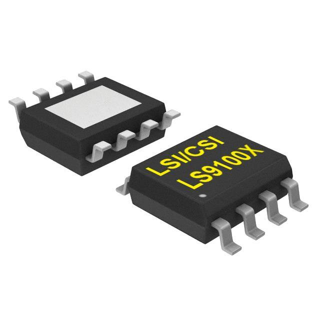
LS9100
Dimmable High Voltage LED Archimedes Series
Direct AC Driver
Features
•
•
•
•
•
•
•
•
•
Integrated Bridge Rectifier and MOSFET Driver
Wide AC input range up to 310 Vac 50/60Hz
50mA DC output current
Ultra simple circuit solution. Requires Only One R
passive component
Thermal Turndown Protections
Voltage Shutdown Protections
Thermal Enhanced SOP-8 and Heat Sink PAD package
TRIAC Dimmable (Leading/Trailing Edge)
Programmable LED Current with an external sense
resistor
Applications
•
•
•
•
L1
1
8
L2
RS0
2
7
HS
RS1
3
6
LS1
RS2
4
5
LS0
LED Driver
Current Source limiter
General Illumination
Commercial and Industrial Lighting
Description
The LS9100 is a High Voltage full-bridge rectifier combined with a current limiter source
circuit and protection circuit. Its rugged design is optimized for driving LED banks directly
from the main utility line eliminating external components by merging them into a
monolithic package, drastically reducing the board space and cost. The thermal turndown
located in the center of the IC protects itself from operating in atypical conditions. The
voltage shutdown protection circuit safeguards the IC and the system’s LEDs from voltage
surges that can overstress the system.
Ordering Information
Part Number
Description
LS9100X-S
LS9100X-STR
SOP-8: Tape and Reel (1000/Reel)
LS9100-170306-A-1
© 2016 LSI Computer Systems, Inc.
�PIN Configuration
L1
1
8
L2
RS0
2
7
HS
RS1
3
6
LS1
RS2
4
5
LS0
Top View
PIN
#
Name
Description
1
L1
Input 1 AC
2
RS0
Current sense resistor input 0
3
RS1
Current sense resistor input 1
4
RS2
Current sense resistor input 2
5
LS0
Low Side input 0
6
LS1
Low Side input 1
7
HS
High side output
8
L2
Input 2 AC
PAD
xPAD
Current sense resistor input 0
Block Diagram
HS
7
LS0
5
High Voltage
Protection
Ckt
L1
1
Current
Control
Ckt
Bridge Rectifier
Ckt
L2
8
LS9100
LS9100-170306-2
LS1
6
Thermal
Turndown
Ckt
RS0
2
RS1
3
RS2
4
�Maximum Rating And Electrical Characteristics
Rating at 25°C ambient temperature unless otherwise specified (Note).
Parameter
Symbol
Min
Typ
Max
Unit
Repetitive peak reverse voltage (Input L1-L2)
Vrrm
500
V
DC Blocking voltage (Input L1-L2)
Vdc
500
V
RMS Voltage (Input L1-L2)
Vrms
310
V
Instantaneous forward voltage (L1-2/HV)
Vf
Average forward current (L1-2/HV)
Iav
50
mA
Peak Forward surge current (Note 2)
Ifsm
80
mA
DC reverse current
@TA=25°C
@TA=100°C
Ir
.5
1.00
uA
Low Side peak voltage (Input LS0-1)
Vls
100
350
V
130
145
V
50
140
mA
Low Side Voltage Shutdown Protection
(Input LS0-1)
Vshdw
0.75
115
Total Low Side Current (Input LS0-1)
V
Package Power Dissipation (Note 3)
PDpkd
2500
mW
Typical Thermal resistance (Note 3)
Rɵja
45
°C/W
Typical Junction capacitance (PIN 1,8)
Cj
Operating Junction Temperature
Tj
Current Thermal turndown
Itdw
Storage temperature
Tstrg
Junction Temperature
Lead Temperature (10 second soldering)
45
-40
pF
+125
-0.32
-55
%A/°C
+125
°C
Tjmax
+150
°C
Tsld
+300
°C
Notes:
1. Stresses above these ratings may cause permanent damage. Exposure to absolute maximum
conditions for extended periods may degrade device reliability.
2. 1msec half sine wave superimposed on rated load
3. Power dissipated from junction to lead PCB mounted on suggested PAD Layout. Derate 20mW/°C
when the ambient temperature is above 25 °C. Special care of the thermal dissipation in the PCB
design must be taken.
4. ESD protection. HBM : 1kV at all Pins.
LS9100-170306-3
°C
�Electrostatic Discharge Sensitivity
This integrated circuit can be damaged by ESD. LSI/CSI recommends
that all integrated circuits be handled with appropriate
precautions. Failure to observe proper handling and installation
procedures can cause damage. ESD damage can range from subtle
performance degradation to complete device failure. Precision
integrated circuits may be more susceptible to damage because
very small parametric changes could cause the device not to meet
its published specifications.
7
6
5
HS
LS1
LS0
RS0
RS1
RS2
2
3
4
L
8
N
L2
Surge
Protection
CKT
L1
110VAC
60HZ
1
Typical Application
Rsns
DANGER!: THE READER IS WARNED THAT
CAUTION MUST BE USED IN THE CONSTRUCTION,
TESTING AND USE OF THIS CIRCUIT. LETHAL HIGH
VOLTAGE POTENTIALS ARE PRESENT IN THIS
CIRCUIT. EXTREME CAUTION MUST BE USED IN
WORKING WITH, AND MAKING CONNECTIONS
TO, THIS CIRCUIT. USE CAUTION.
LS9100-170306-4
�Typical Characteristics
At Tamb = + 25, unless otherwise noted.
Output Current (Icsns) vs. External Resistor (Rcsns)
Tj,+125°C
Tj,+85°C
100
Tj,+25°C
Tj, 0°C
Rcsns (Ω)
Tj,-40°C
10
1
1
10
100
Icsns (mA)
Total Power Dissipation (mW) vs. Ambient Temperature (Ta)
3000
Power Dissipation (mW)
2500
2000
1500
1000
500
0
0
20
40
60
Ambient Temperature (°C)
LS9100-170306-5
80
100
120
�Package Information 8-Lead SOP Exposed Pad Plastic Package
Notes:
A. All linear dimension are in inches.
B. The thermal pad is design to be solder on the PCB.
C. This drawing is subject to change without notice.
LS9100-170306-6
�Package Mounting
The figure below provides the minimum
recommended PCB layout for the LS9100
device. For lowest overall thermal resistance, it
is best to solder the heat sink Pad directly to
the circuit board. Adding more area to the
heat sink improves heat dissipation.
0.05
0.600
Solder mask
over copper
0.112
Top Side 0.096
0.05
0.05
0.600
0.022
10x 0.012
Via Plated
holes
0.132
Bottom Side
0.600
Notes:
A. All linear dimension are in inches (not to scale).
B. This drawing is subject to change without notice.
C. This package mounting is a guideline example and does not cover all applications.
D. Conformal Coating material must be applied to act as protection against moisture and harsh
environments.
LS9100-170306-7
�IMPORTANT NOTICE
The information included herein is believed to be accurate and reliable. However, LSI Computer
Systems, Inc. assumes no responsibilities for inaccuracies, nor for any infringements of patent
rights of others which may result from its use. LSI Computer Systems reserves the right to change
circuitry and specifications at any time without notification to the customer. LSI Computer
Systems assumes no liability for applications assistance or the design of Buyers’ products. Buyers
are the only responsible for their products and applications using LSI Computer Systems
components. To minimize the risks associated with Buyers’ products and applications, Buyers
should provide adequate design and operating safeguards.
LS9100-170306-8
�
很抱歉,暂时无法提供与“LS9100X-S”相匹配的价格&库存,您可以联系我们找货
免费人工找货