IS31FL3801
Smart Integrated Matrix LED Driver with Touch Key Controller
GENERAL DESCRIPTION
FEATURES
The IS31FL3801 is a general purpose 16×8 or 15×9 LED
Matrix programmed via 1MHz I2C compatible interface.
Each LED can be dimmed individually with 8-bit PWM
data, and each CSx has 8-bit DC scaling (Color
Calibration) data which allowing 256 steps of linear PWM
dimming for each dot and 256 steps of DC current
adjustable level for each CSx.
Matrix LED Driver
Supply voltage range: 2.7V to 5.5V
16 current sinks
Support 16×n (n=1~8), 15×9 LED matrix
configurations
Individual 256 PWM control steps
256 DC current steps for each CSx
64 global current steps
SDB rising edge reset I2C module
32kHz PWM frequency
1MHz I2C-compatible interface
Individual open and short error detect function
PWM 180 degree phase shift
Spread spectrum
De-ghost
Capacitive Touch Sensor
Capacitive touch controller with readable key
value through shared GPIO
Individual sensitivity threshold setting for each
touch key
Optional multiple-key function
Press and hold function
Automatic calibration
Individual key calibration
Interrupt output with auto-clear and repeating
Auto sleep mode for extremely low power
Key wake up from sleep mode
400kHz fast-mode I²C interface
Provides Spread
Operating temperature between -40°C ~ +105°C
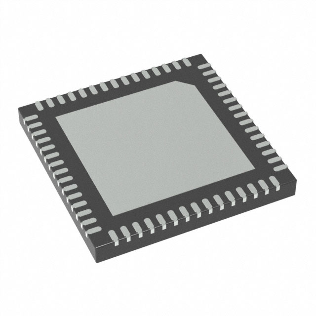
QFN-60 package
Additionally each LED open and short state can be
detected, IS31FL3801 store the open or short information
in Open-Short Registers. The Open-Short Registers
allowing MCU to read out via I2C compatible interface.
Inform MCU whether there are LEDs open or short and
the locations of open or short LEDs.
An eleven-channel capacitive touch controller is
integrated with on-chip calibration logic which
continuously monitors the environment and automatically
adjusts the threshold levels to prevent false triggers.
An on-chip I²C slave controller with 400kHz capability and
programmable slave addresses serves as the
communication port for the host MCU. An interrupt, INTB,
can be configured so it is generated when a trigger event
(touched or released) occurs. Trigger or clear condition
can be configured by setting the interrupt register.
IS31FL3801 is available in RoHS compliant package
QFN-60 (7mm×7mm). It operates from 2.7V to 5.5V over
the temperature range of -40°C to +105°C.
APPLICATIONS
Lumissil Microsystems – www.lumissil.com
Rev. 0B, 08/14/2020
Home appliance touch control keys
Industrial applications
Gaming devices
IoT devices
1
�IS31FL3801
BLOCK DIAGRAM
Block Diagram of IS31FL3801
Lumissil Microsystems – www.lumissil.com
Rev. 0B, 08/14/2020
2
�IS31FL3801
PACKAGE TYPE
Lumissil Microsystems – www.lumissil.com
Rev. 0B, 08/14/2020
3
�IS31FL3801
PIN CONFIGURATION
No.
Pin
Description
23
ISET
An external resistor to ground is required for setting the LED
current
1-3, 5-8, 52, 54-60
CS1-CS15
Current sinks for LED matrix
4, 14, 21, 22, 26, 33, 34,
41, 44-47, 53
VSS
Ground connection
19, 20, 24, 49
VDD
25
INTB
Power supply. Typical decoupling capacitors of 0.1uF and 10uF should
be connected between VDD and VSS
Interrupt output, active low.
27
AD
I2C address setting.
28-32,37-40,42-43
KEY0-KEY10
Input sense channel 0 -10
35
SDA
I2C data, need to pull up with 4.7K resistor
36
SCL
48
VDDC
50
RSTN
51
CREF
I2C clock, need to pull up with 4.7K resistor
Internal regulator output around 1.8V. Typical decoupling capacitors of
0.1uF and 10uF should be connected between VDDC and VSS
Low active. A resistor to VDD and a capacitor to VSS are typically
connected.
RSTN is pulled low when LVR occurs. The threshold of RSTN is set at
0.3VDD. RSTN is also used for special test mode and writer mode
entry.
External capacitor must be connected for touch key controller.
10-13, 15-18
SW8-SW1
Power SW.
9
CS16/SW9
Current sinks for LED matrix CS16 or power switch SW9
Lumissil Microsystems – www.lumissil.com
Rev. 0B, 08/14/2020
4
�IS31FL3801
ORDERING INFORMATION
Industrial Range: -40°C to +105°C
Order Part No.
Package
QTY
IS31FL3801-QFLS3-TR
QFN-60, Lead-free
2500
Copyright © 2020 Lumissil Microsystems. All rights reserved. Lumissil Microsystems reserves the right to make changes to this specification and its products
at any time without notice. Lumissil Microsystems assumes no liability arising out of the application or use of any information, products or services
described herein. Customers are advised to obtain the latest version of this device specification before relying on any published information and before
placing orders for products.
Lumissil Microsystems does not recommend the use of any of its products in life support applications where the failure or malfunction of the product can
reasonably be expected to cause failure of the life support system or to significantly affect its safety or effectiveness. Products are not authorized for use in
such applications unless Lumissil Microsystems receives written assurance to its satisfaction, that:
a.) the risk of injury or damage has been minimized;
b.) the user assume all such risks; and
c.) potential liability of Lumissil Microsystems is adequately protected under the circumstances
Lumissil Microsystems – www.lumissil.com
Rev. 0B, 08/14/2020
5
�IS31FL3801
TYPICAL APPLICATION CIRCUIT (QFN-60)
Figure 1 Typical Application Circuit (QFN-60)
Note 1: The chip should be placed far away from the noise points in order to prevent the EMI.
Note 2: The RS and CS should place as close to the chip as possible to reduce EMI.
Lumissil Microsystems – www.lumissil.com
Rev. 0B, 08/14/2020
6
�IS31FL3801
1.
DETAILED DESCRIPTION
1.1
IS31FL3801 GUI
IS31FL3801 GUI is a windows-based Integrated Design Environment (IDE). User can use it to develop touch key
applications without firmware coding. With the GUI user can design the touch key system easily. With the GUI you
can:
1. Monitor the Key value
2. Set touch threshold and enable keys
3. Switch the operating modes
4. Tune System parameters
5. Touch Key and GPIO Configuration
6. Matrix LED demo
7. Set Slider Electrodes
Lumissil Microsystems – www.lumissil.com
Rev. 0B, 08/14/2020
7
�IS31FL3801
Lumissil Microsystems – www.lumissil.com
Rev. 0B, 08/14/2020
8
�IS31FL3801
Please refer to the User’s Guide for other details.
Lumissil Microsystems – www.lumissil.com
Rev. 0B, 08/14/2020
9
�IS31FL3801
ABSOLUTE MAXIMUM RATINGS
Supply voltage, VCC (for LED driving)
-0.3V ~ +6.0V
Supply voltage, VDD
+5.5V
Voltage at any input pin
-0.3V ~ VCC+0.3V
Maximum junction temperature, TJMAX
+150°C
Storage temperature range, TSTG
-65°C ~ +150°C
Operating temperature range, TA=TJ
-40°C ~ +105°C
Junction Package thermal resistance, junction to ambient (4 layer standard
test PCB based on JESD 51-2A), θJA
35°C/W
ESD (HBM)
±2kV
ESD (CDM)
±750V
Note 4: Stresses beyond those listed under “Absolute Maximum Ratings” may cause permanent damage to the
device. These are stress ratings only and functional operation of the device at these or any other condition beyond
those indicated in the operational sections of the specifications is not implied. Exposure to absolute maximum rating
conditions for extended periods may affect device reliability.
1.2
ELECTRICAL CHARACTERISTICS
TA = 25°C, VDD = 2.7V ~ 5.5V, unless otherwise noted. Typical value are T A = 25°C, VDD = 5V.
Symbol
Parameter
Condition
Min.
Typ.
2.7
Max.
Unit
5.5
V
VDD
Supply voltage
IOUT
Maximum constant current of CSy
RISET =10kΩ, GCC=0xFF
SL=0xFF
34.5
mA
IDD, stop
Quiescent power supply current
VDD = 5.5V
2.5
mA
mA
Electrical Characteristics (LED Driver)
Average current on each LED
ILED = IOUT(PEAK)/Duty(4.14)
RISET =10kΩ, GCC=0xFF
SL=0xFF
4.22
Current switch headroom voltage
SWx
ISWITCH=612mA RISET =10kΩ,
GCC=0xFF, SL=0xFF
450
Current sink headroom voltage CSy
ISINK=34mA, RISET =10kΩ,
GCC=0xFF, SL=0xFF
250
tSCAN
Period of scanning
(Note 5)
33
µs
tNOL1
Non-overlap blanking time during
scan, the SWx and CSy are all off
during this time
0.83
µs
tNOL2
Delay total time for CS1 to CS 18,
during this time, the SWx is on but
CSy is not all turned on
0.3
µs
ILED
VHR
(Note 6)
mV
Electrical Characteristics (Touch Key)
∆CS
Normal detectable capacitance
40
pF
tscan, TK
Period of scanning for 11 Touch
Key channels
55
mS
Lumissil Microsystems – www.lumissil.com
Rev. 0B, 08/14/2020
10
�IS31FL3801
1.3
I2C SWITCHING CHARACTERISTICS
Symbol
fSCL
tBUF
tHD, STA
tSU, STA
tSU, STO
tHD, DAT
tSU, DAT
tLOW
tHIGH
tR
tF
IOL
Parameter
Serial-Clock frequency
Bus free time between a STOP and
a START condition
Hold time (repeated) START
condition
Repeated START condition setup
time
STOP condition setup time
Data hold time
Data setup time
SCL clock low period
SCL clock high period
Rise time of both SDA and SCL
signals, receiving
Fall time of both SDA and SCL
signals, receiving
Low level sink current
Condition
Min.
Typ.
Max.
Unit
400
kHz
1.3
μs
0.6
μs
0.6
μs
0.6
0.9
100
1.3
0.7
(Note 7)
(Note 7)
20+0.
1Cb
20+0.
1Cb
10
μs
μs
ns
μs
μs
300
ns
300
Ns
mA
VIH
Logic “0” input voltage
VDD = 5.5V
1.4
V
VIL
Logic “0” input voltage
VDD = 2.7V
0.4
V
Note 5: The period of SWx is turned on.
Note 6: Guaranteed by design.
Note 7: Cb = total capacitance of one bus line in pF. ISINK ≤ 6mA. tR and tF measured between 0.3 × VDD and 0.7 ×
VDD.
Lumissil Microsystems – www.lumissil.com
Rev. 0B, 08/14/2020
11
�IS31FL3801
1.4
I2C INTERFACE
IS31FL3801 uses a serial bus, which conforms to the I2C protocol, to control the chip’s functions with two wires: SCL
and SDA. IS31FL3801 has a 7-bit slave address (A7:A1), followed by the R/W bit, A0. Set A0 to “0” for a write
command and set A0 to “1” for a read command. The value of bits A1 and A2 are determined by the connection of the
AD pin, to GND, 1/3 VDD, 2/3VDD, and VDD.
The complete slave address is:
Bit
A7:A3
A2:A1
A0
Value
01101
AD
1/0
AD connected to GND, AD = 00;
AD connected to 1/3VDD, AD = 01;
AD connected to 2/3VDD = 10;
AD connected to VDD = 11;
AD pin can also be configured as a Touch Key channel. When then AD pin is used for a Touch Key channel, A2: A1 =
00.
The SCL and SDA are open-drain IO so an external pull-up resistor (typically 4.7kΩ) is required. The maximum clock
frequency specified by the I2C standard is 400kHz. In this discussion, the master is the host microcontroller and the
slave is IS31FL3801.
The timing diagram for the I2C is shown in Figure 2. When there is no interface activity, both the SDA and SCL should
be held high.
The “START” signal is generated by lowering the SDA signal while the SCL signal is high. The start signal will alert all
devices attached to the I2C bus to check the incoming address against their own chip address.
The 8-bit chip address is sent next, most significant bit first. Each address bit must be stable while the SCL level is
high.
After the last bit of the chip address is sent, the master checks for IS31FL3801’s acknowledge. The master releases
the SDA line which gets pulled to high (through a pull-up resistor). Then the master sends an SCL pulse. If
IS31FL3801 has received the address correctly, it holds the SDA line low during the SCL pulse. If the SDA line is not
low, the master should send a “STOP” signal (discussed later) and abort the transfer.
Following acknowledge of IS31FL3801, the header byte is sent, most significant bit first. IS31FL3801 must generate
another acknowledge indicating that the header has been received.
Following acknowledge of IS31FL3801, the commands or register address byte is sent, most significant bit first.
IS31FL3801 must generate another acknowledge indicating that the register address has been received.
Then 8-bit of data byte are sent next, most significant bit first. Each data bit should be valid while the SCL level is
stable high. After the data byte is sent, IS31FL3801 must generate another acknowledge to indicate that the data was
received.
The “STOP” signal ends the transfer. To signal “STOP”, the SDA signal goes high while the SCL signal is high.
SDA
tSU,DAT
tLOW
SCL
tHD,DAT
S
tHIGH
tSU,STA
tHD,STA
R
tSU,STO
tBUF
P
tHD,STA
tR
tF
Start Condition
Restart Condition
Stop Condition
Start Condition
Figure 2 Interface Timing
1.5
READING PORT REGISTERS
____
To read the device data, the bus master must first send to IS31FL3801’s address with the R/ W bit set to “0”, followed
by the header byte. The address of the register of interest is then specified. And then the bus master must then send
____
to IS31FL3801’s address with the R/W bit set to “1”. Data from the register defined by the command byte is then sent
from IS31FL3801 to the master.
Lumissil Microsystems – www.lumissil.com
Rev. 0B, 08/14/2020
12
�IS31FL3801
1.6
I2C Command Format
In the I2C bus, some devices are masters, and they have to generate the bus clock and initiate communication. To
select the IS31FL3801 device, they must choose the right slave address and follow it by a header. If the header is
55h, the commands and data that follows are for the matrix LED driver. If the header is AAh, the commands and data
that follows are for the Touch Key controller. If the header is A5h, IS31FL3801 will immediately save the current data
in the registers. Saved data will become the default value of IS31FL3801.
First byte
Second
byte
Slave
address
Header
55h
Bit
Value
Other bytes
Ending
Matrix LED Commands and
data
Stop signal
A7:A3 A2:A1 A0
01101
AD
SCL High
1/0
SDA Rising edge
AAh
Touch Key Commands and
data
Stop signal
A5h
A special header is no
following bytes. It is used for
saving parameters
Stop signal
Two examples for the I2C Command are as follows:
The waveforms of Touch Key Commands for Write data.
The waveforms of Touch Key Commands for Read data.
1.7
Matrix LED Operation
Register Definition
Address
Name
Function
Table
R/W
Default
01h~8Fh
PWM Register
Set PWM value for LED
6
W
0000 0000
90h~9Fh
Scaling Register
Control the DC output current of each
CSy
7
W
0000 0000
A0h
Configuration Register
Configure the operation mode
8
W
0000 0000
A1h
Global Current Control
Register
Set the global current
9
W
0000 0000
B0h
Pull Down/Up Resistor
Selection Register
Set the pull down resistor for SWx and
pull up resistor for CSy
10
W
0011 0011
Lumissil Microsystems – www.lumissil.com
Rev. 0B, 08/14/2020
13
�IS31FL3801
B1h
Spread Spectrum Register
Spread spectrum function enable
11
W
0000 0000
B2h
PWM Frequency Register
Set the PWM frequency
12
W
0000 0001
Open/Short Register
Store the open or short information
13
W
0000 0000
Reset Register
Reset all register to POR state
-
W
0000 0000
B3h~C4h
CFh
PWM Register
PWM Register 16x8
PWM Register 15x9
Figure 3 PWM Register
Lumissil Microsystems – www.lumissil.com
Rev. 0B, 08/14/2020
14
�IS31FL3801
01h ~ 8Fh PWM Register
Bit
D7:D0
Name
Default
PWM
0000 0000
Each dot has a byte to modulate the PWM duty in 256 steps.
The value of the PWM Registers decides the average current of each LED noted ILED.
ILED computed by Formula (1):
I LED
PWM
I OUT ( PEAK ) Duty (1)
256
Where Duty is the duty cycle of SWx,
Duty
30s
1
1
30s 0.8s 0.27 s 9 9.32
(2)
IOUT is the output current of CSy (y=1~16),
I OUT ( PEAK )
342 GCC SL
RISET 64 256
(3)
GCC is the Global Current Control Register (A1h) value, SL is the Scaling Register value as below and RISET is the
external resistor of ISET pin. D[n] stands for the individual bit value, 1 or 0, in location n.
For example: if D7:D0=1011 0101 (0xB5, 181), GCC= 100 0000, RISET=10kΩ, SL=1111 1111:
I LED
342
64 255
1
181
10k 64 256 9.32 256
Scaling Register
Figure 4 Scaling Register
Lumissil Microsystems – www.lumissil.com
Rev. 0B, 08/14/2020
15
�IS31FL3801
90h ~ 9Fh Scaling Register
Bit
D7:D0
Name
SL
Default
0000 0000
Scaling register control the DC output current of each dot. Each dot has a byte to modulate the scaling in 256 steps.
The value of the Scaling Register decides the peak current of each LED noted I OUT(PEAK). IOUT(PEAK) computed by
Formula (3).
A0h Configuration Register
Bit
D7:D4
D3
D2:D1
D0
Name
SWS
LGC
OSDE
SSD
Default
0001
0
00
0
The Configuration Register sets operating mode of IS31FL3801.
SSD
0
1
Software Shutdown Control
Software shutdown
Normal operation
OSDE Open Short Detection Enable
00
Disable open/short detection
01/11 Enable open detection
10
Enable short detection
LGC
0
1
H/L logic
1.4V/0.4V
2.4V/0.6V
SWS
0000
0001
0010
0011
0100
0101
0110
0111
1000
Others
SWx Setting
n=9, SW1~SW9, 9SW×15CS matrix
n=8, SW1~SW8, 8SW×16CS matrix
n=7, SW1~SW7, 7SW×16CS matrix, SW8 no-active
n=6, SW1~SW6, 6SW×16CS matrix, SW7~SW8 no-active
n=5, SW1~SW5, 5SW×16CS matrix, SW6~SW8 no-active
n=4, SW1~SW4, 4SW×16CS matrix, SW5~SW8 no-active
n=3, SW1~SW3, 3SW×16CS matrix, SW4~SW8 no-active
n=2, SW1~SW2, 2SW×16CS matrix, SW3~SW8 no-active
SW1~SW9 with same phase, all on.
SW1~SW9, SW1~SW9, 9SW×15CS matrix
When OSDE set to “01”, open detection will be trigger once, the user could trigger open detection again by set OSDE
from “00” to “01”.
When OSDE set “10”, short detection will be trigger once, the user could trigger short detection again by set OSDE
from “00” to “10”.
When SSD is “0”, IS31FL3801 works in software shutdown mode and to normal operate the SSD bit should set to “1”.
SWS control the duty cycle of the SWx, default mode is 1/8.
Lumissil Microsystems – www.lumissil.com
Rev. 0B, 08/14/2020
16
�IS31FL3801
A1h Global Current Control Register
Bit
D7
D6:D0
Name
-
GCC
Default
0
000 0000
The Global Current Control Register modulates all CSy (y=1~16) DC current which is noted as IOUT in 65 steps,
maximum GCC is “100 0000’, if GCC> “1000000”, GCC= “100 0000”.
IOUT is computed by the Formula (3):
I OUT ( PEAK )
342 GCC SL
RISET 64 256
7
GCC D[n] 2 n
n 0
Where D[n] stands for the individual bit value, 1 or 0, in location n.
B0h Pull Down/Up Resistor Selection Register
Bit
D7
D6:D4
D3
D2:D0
Name
PHC
SWPDR
-
CSPUR
Default
0
011
0
011
Set pull down resistor for SWx and pull up resistor for CSy.
PHC
0
1
Phase choice
0 degree phase delay
180 degree phase delay
SWPDR
000
001
010
011
100
101
110
111
SWx Pull down Resistor Selection Bit
No pull down resistor
0.5kΩ only in SWx off time
1.0kΩ only in SWx off time
2.0kΩ only in SWx off time
1.0kΩ all the time
2.0kΩ all the time
4.0kΩ all the time
8.0kΩ all the time
CSPUR CSy Pull up Resistor Selection Bit
000
No pull up resistor
001
0.5kΩ only in CSx off time
010
1.0kΩ only in CSx off time
011
2.0kΩ only in CSx off time
100
1.0kΩ all the time
101
2.0kΩ all the time
110
4.0kΩ all the time
111
8.0kΩ all the time
Lumissil Microsystems – www.lumissil.com
Rev. 0B, 08/14/2020
17
�IS31FL3801
B1h Spread Spectrum Register
Bit
D7:D6
D4
D3:D2
D1:D0
Name
-
SSP
RNG
CLT
Default
00
0
00
00
When SSP enable, the spread spectrum function will be enabled and the RNG & CLT bits will adjust the range and
cycle time of spread spectrum function.
SSP
0
1
Spread spectrum function enable
Disable
Enable
RNG
00
01
10
11
CLT
00
01
10
11
Spread spectrum range
±5%
±15%
±24%
±34%
Spread spectrum cycle time
1980μs
1200μs
820μs
660μs
B2h PWM Frequency
Bit
D7:D3
D2:D0
Name
-
PWMF
Default
00000
001
Set the PWM frequency, default is 32 kHz. In order to avoid LED display flicker, it is recommended PWM frequency ÷
n is higher than 100Hz, so when PWM frequency is 0.5 kHz, n cannot be more than 4, when PWM frequency is 0.25
kHz, n cannot be more than 2.
PWMF
000
001
010
011
100
101
110
111
PWM frequency setting
55kHz
32kHz
4kHz
2kHz
1kHz
0.5kHz, (n≤4)
0.25KHz, (n≤2)
80kHz
Lumissil Microsystems – www.lumissil.com
Rev. 0B, 08/14/2020
18
�IS31FL3801
B3h~C4h Open/Short Register (Read Only)
Bit
D7:D0
Name
CS16:CS09, CS08:CS01
Default
0000 0000
When OSDE (A0h) is set to “01”, open detection will be trigger once, and the open information will be stored at
B3h~C4h.
When OSDE (A0h) set to “10”, short detection will be trigger once, and the short information will be stored at
B3h~C4h.
Before set OSDE, the GCC should set to 0x01.
Figure 5 Open/Short Register
CFh Reset Register
Once user writes the Reset Register with 0xAE, IS31FL3801 will reset all the IS31FL3801 registers to their default
value. On initial power-up, the IS31FL3801 registers are reset to their default values for a blank display.
Lumissil Microsystems – www.lumissil.com
Rev. 0B, 08/14/2020
19
�IS31FL3801
APPLICATION INFORMATION
Scanning cycle T=62.14µs((30µs+0.8µs+0.27µs)×2) (n=2)
Scanning cycle T=248.56µs((30µs+0.8µs+0.27µs)×8) (n=8)
SW1
SW2
SW3
SW4
SW5
SW6
SW7
SW8
SW9
CS16
CS1
tNOL2=0.27µs
tSCAN=30µs
tNOL1=0.8µs
Scanning cycle T=279.63µs((30µs+0.8µs+0.27µs)×9) (n=9)
De-Ghost time
PWM Duty is variable from 0/256~255/256
I OUT
342 GCC SL
RISET 256 256
SCANNING TIMING
As shown in Figure above, the SW1~SW9 is turned on by serial, LED is driven 15 by 9 within the SWx (x=1~9) on
time (SWx, x=1~9 is source and it is high when LED on) , including the non-overlap blanking time during scan, the
duty cycle of SWx (active high, x=1~9) is (n=9):
Duty
30s
1
1
30s 0.8s 0.27 s 9 9.32
used the formula (2)
Duty
30s
1
1
30s 0.8s 0.27 s 8 8.29
used the formula (2)
Or (n=8):
Where 30μs is tSCAN, the period of scanning and 0.8μs is tNOL1, the non-overlap time and 0.27μs is the CSx delay time.
PWM CONTROL
After setting the IOUT and GCC, the brightness of each LEDs (LED average current (I LED)) can be modulated with 256
steps by PWM Register, as described in Formula (1).
I LED
PWM
I OUT ( PEAK ) Duty (1)
256
Where PWM is PWM Registers’ (01h~8Fh) data showing in PWM registers.
For example, in Figure 1, if RISET= 10kΩ, PWM= 1011 0101 (0xB5, 181), and GCC= 100 0000, SL= 1111 1111, then,
I OUT ( PEAK )
342 GCC SL
342
64 255
1
181
(n=9)
I LED
RISET 64 256
10k 64 256 9.32 256
Writing new data continuously to the registers can modulate the brightness of the LEDs to achieve a breathing effect.
Lumissil Microsystems – www.lumissil.com
Rev. 0B, 08/14/2020
20
�IS31FL3801
GAMMA CORRECTION
In order to perform a better visual LED breathing effect we recommend using a gamma corrected PWM value to set
the LED intensity. This results in a reduced number of steps for the LED intensity setting, but causes the change in
intensity to appear more linear to the human eye.
Gamma correction, also known as gamma compression or encoding, is used to encode linear luminance to match the
non-linear characteristics of display. Since the IS31FL3801 can modulate the brightness of the LEDs with 256 steps, a
gamma correction function can be applied when computing each subsequent LED intensity setting such that the
changes in brightness matches the human eye's brightness curve.
32 Gamma Steps with 256 PWM Steps
C(0)
C(1)
C(2)
C(3)
C(4)
C(5)
C(6)
C(7)
0
1
2
4
6
10
13
18
C(8)
C(9)
C(10)
C(11)
C(12)
C(13)
C(14)
C(15)
22
28
33
39
46
53
61
69
C(16)
C(17)
C(18)
C(19)
C(20)
C(21)
C(22)
C(23)
78
86
96
106
116
126
138
149
C(24)
C(25)
C(26)
C(27)
C(28)
C(29)
C(30)
C(31)
161
173
186
199
212
226
240
255
256
224
PWM Data
192
160
128
96
64
32
0
0
4
8
12
16
20
24
28
32
Intensity Steps
Figure 6 Gamma Correction (32 Steps)
Choosing more gamma steps provides for a more continuous looking breathing effect. This is useful for very long
breathing cycles. The recommended configuration is defined by the breath cycle T. When T=1s, choose 32 gamma
steps, when T=2s, choose 64 gamma steps. The user must decide the final number of gamma steps not only by the
LED itself, but also based on the visual performance of the finished product.
64 Gamma Steps with 256 PWM Steps
C(0)
C(1)
C(2)
C(3)
C(4)
C(5)
C(6)
C(7)
0
1
2
3
4
5
6
7
C(8)
C(9)
C(10)
C(11)
C(12)
C(13)
C(14)
C(15)
8
10
12
14
16
18
20
22
C(16)
C(17)
C(18)
C(19)
C(20)
C(21)
C(22)
C(23)
24
26
29
32
35
38
41
44
C(24)
C(25)
C(26)
C(27)
C(28)
C(29)
C(30)
C(31)
47
50
53
57
61
65
69
73
C(32)
C(33)
C(34)
C(35)
C(36)
C(37)
C(38)
C(39)
77
81
85
89
94
99
104
109
Lumissil Microsystems – www.lumissil.com
Rev. 0B, 08/14/2020
21
�IS31FL3801
C(40)
C(41)
C(42)
C(43)
C(44)
C(45)
C(46)
C(47)
114
119
124
129
134
140
146
152
C(48)
C(49)
C(50)
C(51)
C(52)
C(53)
C(54)
C(55)
158
164
170
176
182
188
195
202
C(56)
C(57)
C(58)
C(59)
C(60)
C(61)
C(62)
C(63)
209
216
223
230
237
244
251
255
256
224
PWM Data
192
160
128
96
64
32
0
0
8
16
24
32
40
48
56
64
Intensity Steps
Figure 7 Gamma Correction (64 Steps)
Note: The data of 32 gamma steps is the standard value and the data of 64 gamma steps is the recommended value.
OPERATING MODE
IS31FL3801 can only operate in PWM Mode. The brightness of each LED can be modulated with 256 steps by PWM
registers. For example, if the data in PWM Register is “0000 0100”, then the PWM is the fourth step.
Writing new data continuously to the registers can modulate the brightness of the LEDs to achieve a breathing effect.
OPEN/SHORT DETECT FUNCTION
IS31FL3801 has open and short detect bit for each LED.
By setting the OSDE bits of the Configuration Register (A0h) from “00” to “01” or “10”, the LED Open/short Register
will start to store the open/short information and after at least 2 scanning cycles and the MCU can get the open/short
information by reading the B3h~C4h, the open/short data will not get refreshed when setting the OSDE bit of the
Configuration Register.
The two configurations need to set before setting the OSDE bits:
1
. 0x0F≤GCC≤0x40, B0h=0x00
2
. 0x01≤GCC≤0x40, B0h=0x30
Where GCC is the Global Current Control Register (A1h) and both case 1 or two can get the correct open and short
information. B0h is the Pull Down/UP Resistor Selection Register and 0x30 is to enable the SWx pull-up function.
The detect action is one-off event and each time before reading out the open/short information, the OSDE bit of the
Configuration Register (A0h) need to be set from “0” to “1” (clear before set operation).
DE-GHOST FUNCTION
The “ghost” term is used to describe the behavior of an LED that should be OFF but instead glows dimly when another
LED is turned ON. A ghosting effect typically can occur when multiplexing LEDs. In matrix architecture any parasitic
capacitance found in the constant-current outputs or the PCB traces to the LEDs may provide sufficient current to dimly
light an LED to create a ghosting effect.
Lumissil Microsystems – www.lumissil.com
Rev. 0B, 08/14/2020
22
�IS31FL3801
To prevent this LED ghost effect, the IS31FL3801 has integrated Pull down resistors for each SWx (x=1~9) and Pull up
resistors for each CSy (y=1~16). Select the right SWx Pull down resistor (B0h) and CSy Pull up resistor (B0h) which
eliminates the ghost LED for a particular matrix layout configuration.
Typically, selecting the 2kΩ will be sufficient to eliminate the LED ghost phenomenon.
The SWx Pull down resistors and CSy Pull up resistors are active only when the CSy/SWx output working the OFF state
and therefore no power is lost through these resistors.
SHUTDOWN MODE
Shutdown mode can be used as a means of reducing power consumption. During shutdown mode all registers retain
their data.
Software Shutdown
By setting SSD bit of the Configuration Register (A0h) to “0”, the IS31FL3801 will operate in software shutdown mode.
When the IS31FL3801 is in software shutdown, all current sources are switched off, so that the matrix is blanked. All
registers can be operated. Typical current consume is 3μA.
Hardware Shutdown
The chip enters hardware shutdown when the SDB pin is pulled low. All analog circuits are disabled during hardware
shutdown, typical the current consume is 3μA.
The chip releases hardware shutdown when the SDB pin is pulled high. During hardware shutdown state Function
Register can be operated.
If VCC has risk drop below 1.75V but above 0.1V during SDB pulled low, please re-initialize all Function Registers
before SDB pulled high.
LAYOUT
As described in external resistor (RISET), the chip consumes lots of power. Please consider below factors when layout
the PCB.
1. The VCC capacitors need to close to the chip and the ground side should well connected to the GND of the chip.
2. RISET should be close to the chip and the ground side should well connect to the GND of the chip.
3. The thermal pad should connect to ground pins and the PCB should have the thermal pad too, usually this pad
should have 9 or 16 via thru the PCB to other side’s ground area to help radiate the heat. About the thermal pad size,
please refer to the land pattern of each package.
4. The CSy pins maximum current is 35mA (RISET=10kΩ), and the SWx pins maximum current is larger, the width of
the trace, SWx should have wider trace then CSy.
Lumissil Microsystems – www.lumissil.com
Rev. 0B, 08/14/2020
23
�IS31FL3801
1.8
Touch Key Operation
Register Function
Address
Name
Function
Controls general power states and power
dissipation
00h
Main Control Register
01h
INT Configuration Register
Interrupt configuration
02h
03h
Key Status Register 1
Key Status Register 2
04h
Interrupt Enable Register 1
05h
Interrupt Enable Register 2
Key0~Key7 status bits
Key8~Key10 status bits
Key0~key7 Enables Interrupts associated
with capacitive touch sensor inputs
Key8~key10 Enables Interrupts associated
with capacitive touch sensor inputs
06h
Key Enable Register 1
Key0~key7 sets the channels enable
07h
Key Enable Register 2
Key8~key10 sets the channels enable
09h
Multiple Touch Key Configure
Register
Auto-Clean Interrupt Register
0Ah
Interrupt Repeat Time Register
Set repeat cycle for pressing key interrupt
0Bh
Auto-SLEEP Mode Register
Set auto enter SLEEP Mode time
0Ch
0Dh
Exit SLEEP Mode Register 1
Exit SLEEP Mode Register 2
Gain and Press Time Setting
Register
Key Touch Sampling Configure
Register
Set press Key0~Key7 to exit SLEEP Mode
Set press Key8~Key10 to exit SLEEP Mode
08h
0Eh
0Fh
Force Calibration Register 1
Force Calibration Register 2
13h
Noise Threshold Register
Set noise threshold value
14h
Noise Indication Register 1
Key0~Key7 noise indication
15h
Noise Indication Register 2
17h
Negative Threshold Register
Key8~key10 noise indication
Set negative threshold and compel calibration
threshold
18h
Wake Up Threshold Register
Set wake up threshold
19h
Scan Voltage Register
Set scanning voltage
1Ah
Scan Frequency Register 1
Set the first and second scanning frequencies
1Bh
Scan Frequency Register 2
Set the third and fourth scanning frequencies
Keys value setting
Keys threshold setting
0000
0000
0000
0000
R/W
0000
1111
0011
1111
0000
0000
0010
1100
0010
0100
0011
0000
Set sampling times and cycle time
11h
12h
Default
0000
0000
0000
1000
1111
1111
0000
0111
1111
1111
0000
0111
Set gain and pressing trigger time
Set auto-calibration cycle and negative value
trigger setting
Key0~Key7 calibration enable forcibly
Key8~Key10 calibration enable forcibly
Lumissil Microsystems – www.lumissil.com
Rev. 0B, 08/14/2020
R
Set auto-clean interrupt time and enable
Calibration Configure Register
KEY0~KEY10 Variation Value
Register
KEY0~KEY10 Threshold Set
30h~3Ah
Register
R/W
Multiple touch key function setting
10h
20h~2Ah
R/W
0000
0000
0011
0010
R
R/W
R
R/W
0000
0000
0000
1001
0000
0101
0111
0000
0111
0011
1011
1000
0000
0000
0011
0000
24
�IS31FL3801
40h,42h
…
52h,54h
41h,43h
…
53h,55h
60h
61h
KEY0~KEY10 Calibration Low
Bit Register
Internal calibration low 8-bit for KEY0~KEY10
R
KEY0~KEY10 Calibration High
Bit Register
Internal calibration high 8-bit for
KEY0~KEY10
GPIO Enable Register 1
GPIO Enable Register 2
Key0~key7 sets the GPIO enable
Key8~key10 sets the GPIO enable
62h
63h
GPIO Value Register 1
GPIO Value Register 2
Key0~key7 set the GPIO values
Key8~key10 set the GPIO values
64h
Slider Enable Register 1
Key0~key7 sets the slider enable
65h
Slider Enable Register 2
Key8~key10 sets the slider enable
66h
67h
Slider Status Register1
Slider Status Register2
Slider status reply1
Slider status reply2
68h
Slider Status Register3
Slider status reply3
69h
Key position 1-2 of Slider1
Shows the position of Slider1
0000
0000
R/W
1110
0000
0000
0111
R
R/W
6Ah
Key position 3-4 of Slider1
Shows the position of Slider1
6Bh
Key position 5-6 of Slider1
Shows the position of Slider1
6Fh
Version Control Register
Shows the firmware version
70h~75h Slider Calibration Register 1-6
76h
0000
0000
R
Slider calibration from the first Key to the sixth
Key
Spread Spectrum Configuration Spread spectrum setting
R/W
0000
0000
1000
0000
0101
0110
0111
1000
1001
1010
0100
0000
0001
0101
0000
0000
00h Main Control Register (Write Only)
Bit
Name
Default
SR
0
1
SDM
0
1
SP
0
1
D7
D6
SR
0
0
System Reset
Normal Mode
System Reset
Shutdown Mode
Normal Mode
Shutdown Mode
Sleep Mode
Normal Mode
SLEEP Mode
D5
D4
D3
D2:D0
SDM
0
SP
0
0
000
00h Main Control Register (Read Only)
Bit
Name
Default
PID
Default
D7:D0
PID
0X31
Product ID, It is read only. User cannot modify the value.
0X31
Lumissil Microsystems – www.lumissil.com
Rev. 0B, 08/14/2020
25
�IS31FL3801
01h Interrupt Configuration Register
Bit
D7:D4
D3
D2
INM
0
D1
D0
Name
MDEND
INE
Default
0000
1
0
0
MDEN
Maximum Duration Time Enable
0
Disable
1
Enable
Maximum press function is used to prevent key pressing all the time by accident. When maximum press function is
enabled, once key keep pressing at programmed time the key calibration value will be updated.
INM
Interrupt Mode
0
Interrupt Mode 0(Touch key trigger once interrupt)
1
Interrupt Mode 1(Touch key trigger repeated interrupt)
INM bit sets interrupt time for once or multiple. Multiple interrupt is used for key pressing detection.
INE
0
1
Interrupt Function Enable
Disable
Enable
02h Key Status Register 1 (Read only)
Bit
D7:D0
Name
KS[7:0]
Default
0000 0000
03h Key Status Register 2 (Read only)
Bit
D7:D3
D2:D0
0000 0
Name
KS[10:8]
Default
000
KS[10:0]
Key0~Key10 Status
0
No action
1
Press or release keys
If the value of KSx is detected over programmed threshold, the corresponding bit will be set to “1”.
04h Interrupt Enable Register 1
Bit
D7:D0
Name
Default
KINT[7:0]
1111 1111
05h Interrupt Enable Register 2
Bit
D7:D3
D2:D0
Name
-
KINT[10:8]
Default
0000 0
111
The Interrupt Enable Register determines whether a sensor pad touch or release (if enabled) causes the interrupt pin
to be asserted.
KINT[10:0]
Key Interrupt Enable
0
Disable
1
Enable
The default value for Interrupt Enable Registers is interrupt enable. Only set INE bit of Interrupt Configuration Register
(01h) to “0”, INTB pin will generate interrupt signal.
Lumissil Microsystems – www.lumissil.com
Rev. 0B, 08/14/2020
26
�IS31FL3801
06h Key Enable Register 1
Bit
D7:D0
Name
Default
KEN[7:0]
1111 1111
07h Key Enable Register 2
Bit
D7:D3
D2:D0
Name
-
KEN[10:8]
Default
KEN[10:0]
0
1
0000 0
Touch Key Enable Setting
Disable
Enable
111
08h Multiple Touch Key Configure Register
Bit
D7:D3
Name
Default
MKEN
0
1
0000 0
Multi- Key Enable
Disable
Enable
MTK[1:0]
01
10
11
Multi -Key Selection
Allow one key triggered at same time
Allow two keys triggered at same time
Allow three keys triggered at same time
D2
D1:D0
MKEN
0
MTK[1:0]
00
D3
D2:D0
ACEN
0
ACT[2:0]
000
09h Auto-Clear Interrupt Register
Bit
Name
Default
ACEN
0
1
D7:D4
0000
Auto-Clear Interrupt Enable
Disable
Enable
ACT[2:0]
Auto-Clear Interrupt Time
000
10ms
001
20ms
010
30ms
011
40ms
100
50ms
101
100ms
110
150ms
111
200ms
When ACEN=0, the INTB will keep low until MCU read 02h and 03h registers. When ACEN=1, if MCU don’t read 02h
and 03h registers within programmed time (ACT=10ms~200ms), INTB pin will be release automatically.
Lumissil Microsystems – www.lumissil.com
Rev. 0B, 08/14/2020
27
�IS31FL3801
0Ah Interrupt Repeat Time Register
Bit
D7:D4
D3:D0
Name
INTRT[3:0]
MPT[3:0]
Default
INTRT[3:0]
0000
0001
0010
0011
0100
0101
0110
0111
1000
1001
1010
1011
1100
1101
1110
1111
0000
Interrupt Repeat Time
Close
50ms
100ms
150ms
200ms
250ms
300ms
350ms
400ms
450ms
500ms
600ms
700ms
800ms
900ms
1s
1111
MPT[3:0]
Multi-key Press Time
0000
Close
0001
50ms
0010
100ms
0011
150ms
0100
200ms
0101
250ms
0110
300ms
0111
350ms
1000
400ms
1001
450ms
1010
500ms
1011
600ms
1100
700ms
1101
800ms
1110
900ms
1111
1s
When set the INM as 1 and several keys are pressed, it will generate the second interrupt until M_PRESS_TIME after
the first interrupt. Then wait for INT_RPT_TIME to trigger the third interrupt. After all of these if the keys are still
pressing, wait for INT_RPT_TIME to trigger others interrupt until keys release.
0Bh Auto-SLEEP Set Register
Bit
D7
D6:D4
D3:D0
Name
ASEN
OSCD[2:0]
AST[3:0]
Default
0
011
1111
ASEN
0
1
Auto-SLEEP Enable
Disable
Enable
OSCD[2:0]
000
Auto-Sleep Oscillator Division
1
Lumissil Microsystems – www.lumissil.com
Rev. 0B, 08/14/2020
28
�IS31FL3801
001
010
011
100
101
110
111
2
4
8
16
32
64
128
AST[3:0]
Auto-SLEEP Time
0000
0.5s
0001
1s
0010
1.5s
0011
2s
0100
2.5s
0101
3s
0110
3.5s
0111
4s
1000
5s
1001
6s
1010
7s
1011
8s
1100
9s
1101
10s
1110
11s
1111
12s
When ASEN=1 and no actions on touch key and I2C interface, the IC will enter into SLEEP Mode after programmed
time (AST).
0Ch Exit SLEEP Mode Register 1
Bit
D7:D1
Name
ESMEN[7:0]
Default
0000 0000
0Dh Exit SLEEP Mode Register 2
Bit
D7:D3
D2:D0
Name
ESMEN[10:8]
Default
0000 0
000
ESMEN[10:0]
Exit Sleep Mode Enable
0
Touch key can’t trigger exiting SLEEP Mode
1
Touch key trigger exiting SLEEP Mode
When IC is in Normal Mode and ASEN=1, set ESMENx=1 will exit from SLEEP Mode by pressing the corresponding
key.
0Eh Gain and Press Time Setting Register
Bit
D7:D4
D3:D0
Name
GAIN[3:0]
MDT[3:0]
Default
0010
1100
GAIN[3:0]
0000
0001
0010
0011
Gain Control
1X
2X
3X
4X
Lumissil Microsystems – www.lumissil.com
Rev. 0B, 08/14/2020
29
�IS31FL3801
0100
5X
0101
6X
0110
7X
0111
8X
1000
9X
1001
10X
1010
11X
1011
12X
1100
13X
1101
14X
1110
15X
1111
16X
The GAIN bits are used to set the gain factor. Internal count will count the final value and put it into KEYx_ΔCOUNT.
MDT[3:0]
Max Duration Time
0000
0.5s
0001
1s
0010
2s
0011
3s
0100
4s
0101
5s
0110
6s
0111
7s
1000
8s
1001
9s
1010
10s
1011
11s
1100
12s
1101
13s
1110
14s
1111
15s
MPT bits set the pressing time. When key pressed continue over the programmed time (MDT), system will force to
calibrate the pressed key. Set MDEN to “1” will enable this function.
0Fh Key Touch Sampling Configure Register
Bit
D7:D4
D3:D2
D1:D0
Name
SC[3:0]
ST[1:0]
CDS[1:0]
01
00
Default
SC[3:0]
0000
0001
0010
0011
0100
0101
0110
0111
1000
1001
1010
1011
1100
1101
1110
1111
0010
Touch Key Sampling Count Setting
1
2
3
4
5
6
7
8
9
10
11
12
13
14
15
16
Lumissil Microsystems – www.lumissil.com
Rev. 0B, 08/14/2020
30
�IS31FL3801
SC is used to set average sampling times for each channel. Higher SC value will increase stability and antiinterference ability, but decrease reaction speed.
ST[1:0]
00
01
10
11
Sampling Time (Single Channel)
1
2
4
8
CDS[1:0]
Cycle Delay Time
00
0ms
01
10ms
10
20ms
11
30ms
Sampling 16 channels is for one cycle.
10h Calibration Configure Register
Bit
D7
D6:D4
D3:D2
D1:D0
Name
-
CSC[2:0]
-
NDC[1:0]
Default
0
011
00
00
CSC[2:0]
Calibrate Sample Count
000
2
001
4
010
8
011
16
100
32
101
64
110
128
111
256
If there is no action on keys, environmental capacitance will be calibrated after CSC times.
NDC[1:0]
Negative Delta Count
00
4
01
8
10
16
11
32
If channel detects the value over negative threshold (NDTH) for NDC times, it will be calibrated forcibly.
11h Force Calibration Register 1
Bit
D7:D0
Name
FCK[7:0]
Default
0000 0000
12h Force Calibration Register 2
Bit
D7:D3
D2:D0
Name
-
FCK[10:8]
Default
0000 0
000
FCK[10:0]
Individual Force Calibrate Key
0
Close
1
Enable
When enable FCKx, the corresponding bit will be set to “0”.
Lumissil Microsystems – www.lumissil.com
Rev. 0B, 08/14/2020
31
�IS31FL3801
13h Noise Threshold Register
Bit
D7:D0
Name
NTH
Default
0011 0010
The noise threshold is from 0~127. It is invalid if NTH>127.
If difference value between samplings is over the programmed threshold, the corresponding noise bit will be set to “1”.
14h Noise Indication Register 1 (Read Only)
Bit
D7:D0
Name
NK[7:0]
Default
0000 0000
15h Noise Indication Register 2 (Read Only)
Bit
D7:D3
D2:D0
Name
-
NK[10:8]
Default
NK[10:0]
0
1
0000 0
000
Noise Indication
No noise
Noise
17h Negative Threshold Register
Bit
D7:D4
D3:D0
Name
NCTH[3:0]
NDTH[3:0]
Default
0000
1001
NCTH[3:0]
0000
0001
0010
0011
0100
0101
0110
0111
1000
1001
1010
1011
1100
1101
1110
1111
Negative Calibrate Threshold Setting
Disabled
-10
-20
-30
-40
-50
-60
-70
-80
-90
-100
-110
-120
Not available
Not available
Not available
NDTH[3:0]
0000
0001
0010
0011
0100
0101
0110
Negative Delta Threshold Setting
-1
-2
-3
-4
-5
-6
-7
Lumissil Microsystems – www.lumissil.com
Rev. 0B, 08/14/2020
32
�IS31FL3801
0111
-8
1000
-9
1001
-10
1010
-11
1011
-12
1100
-13
1101
-14
1110
-15
1111
-16
When negative value is over the programmed threshold (NCTH), the channel will be calibrated forcibly.
If negative value is detected over threshold for NDTH times continually, the channel will be calibrated forcibly.
18h Wake Up Threshold Register
Bit
D7
D6:D0
Name
-
WTH[6:0]
Default
0
Wake up threshold, the range is 0 – 127
000 0101
19h Scan Voltage Register
Bit
D7
D6:D4
D3
D2:D0
Name
VTH
ZERO_Time [2:0]
REFSEL
-
Default
0
111
0
000
VTH
If REFSEL = 0
0
1
If REFSEL = 1
0
1
Scan Voltage
CREF charges to 0.9V
CREF charges to 1.35V
CREF charges to VDDH/2
CREF charges to VDDH*3/4
ZERO_Time [2:0] Discharge time of CREF
000
8 us
001
16 us
010
24 us
011
32 us
100
40 us
101
48 us
110
56 us
111
64 us
REFSEL
0
1
CREF charges source selection
The CREF charging source is 1.8V
The CREF charging source is VDDH
1Ah Scan Frequency Register 1
Bit
D7:D4
D3:D0
Name
SSF[3:0]
FSF[3:0]
Default
0111
0011
FSF[3:0]
0000
0001
First scan frequency
8 MHZ
4 MHZ
Lumissil Microsystems – www.lumissil.com
Rev. 0B, 08/14/2020
33
�IS31FL3801
0010
0011
0100
0101
0110
0111
1000
1001
1010
1011
1100
1101
1110
1111
2.67 MHZ
2 MHZ
1.6 MHZ
1.33 MHZ
1.14 MHZ
1 MHZ
0.89 MHZ
0.8 MHZ
0.73 MHZ
0.67 MHZ
0.62 MHZ
0.57 MHZ
0.53 MHZ
0.5M HZ
SSF[3:0]
0000
0001
0010
0011
0100
0101
0110
0111
1000
1001
1010
1011
1100
1101
1110
1111
Second scan frequency
8 MHZ
4 MHZ
2.67 MHZ
2 MHZ
1.6 MHZ
1.33 MHZ
1.14 MHZ
1 MHZ
0.89 MHZ
0.8 MHZ
0.73 MHZ
0.67 MHZ
0.62 MHZ
0.57 MHZ
0.53 MHZ
0.5M HZ
1Bh Scan Frequency Register 2
Bit
D7:D4
D3:D0
Name
OSF[3:0]
TSF[3:0]
Default
1011
1000
TSF[3:0]
0000
0001
0010
0011
0100
0101
0110
0111
1000
1001
1010
1011
1100
1101
1110
1111
Third scan frequency
8 MHZ
4 MHZ
2.67 MHZ
2 MHZ
1.6 MHZ
1.33 MHZ
1.14 MHZ
1 MHZ
0.89 MHZ
0.8 MHZ
0.73 MHZ
0.67 MHZ
0.62 MHZ
0.57 MHZ
0.53 MHZ
0.5M HZ
Lumissil Microsystems – www.lumissil.com
Rev. 0B, 08/14/2020
34
�IS31FL3801
OSF[3:0]
0000
0001
0010
0011
0100
0101
0110
0111
1000
1001
1010
1011
1100
1101
1110
1111
Fourth scan frequency
8 MHZ
4 MHZ
2.67 MHZ
2 MHZ
1.6 MHZ
1.33 MHZ
1.14 MHZ
1 MHZ
0.89 MHZ
0.8 MHZ
0.73 MHZ
0.67 MHZ
0.62 MHZ
0.57 MHZ
0.53 MHZ
0.5M HZ
20h~2Ah KEY0~KEY10 Variation Value Register (Read Only)
Bit
D7
D6:D0
Name
SIGN
KEYx_ΔCOUNT[6:0]
Default
0
000 0000
SIGB
0
1
KEYx_ΔCOUNT[6:0]
Sign bit
Positive
Negative
Key Value Count
30h~3Ah KEY0~KEY10 Threshold Set Register
Bit
D7
D6:D0
Name
-
KEYx_TH[6:0]
0
011 0000
Default
KEYx_TH[6:0]
0~127
Key Threshold
40h, 42h … 52h, 54h KEY0~KEY10 Calibration Low Byte Register (Read Only)
Bit
D7:D0
Name
KEY0_CAL_L
Default
0000 0000
41h, 43h … 53h, 55h KEY0~KEY10 Calibration High Byte Register (Read only)
Bit
D7:D0
Name
KEY0_CAL_H
Default
0000 0000
60h GPIO Enable Register 1
Bit
D7:D0
Name
GPIOEN[7:0]
Default
0000 0000
Lumissil Microsystems – www.lumissil.com
Rev. 0B, 08/14/2020
35
�IS31FL3801
61h GPIO Enable Register 2
Bit
Name
Default
GPIOEN[10:0]
0
1
D7:D3
D2:D0
GPIOEN[10:8]
0000 0
000
Enable KEY0~KEY10 GPIO Mode
Disable Touch key channel enter GPIO Mode
Enable Touch key channel enter GPIO Mode; A channel cannot be a Touch key or Slider
sensor while it’s was set to be a GPIO.
62h GPIO Value Register 1
Bit
D7:D0
Name
GPV[7:0]
Default
0000 0000
63h GPIO Value Register 2
Bit
Name
Default
GPV[10:0]
0
1
D7:D3
D2:D0
0000 0
62h and 63h registers define the KEY0~KEY10 GPIO values.
GPIO = 0, if the related Enable GPIO Register 1/2 is enabled.
GPIO = 1, if the related Enable GPIO Register 1/2 is enabled.
GPV[10:8]
000
64h Slider Enable Register 1
Bit
D7:D0
Name
SLEN[7:0]
Default
1110 0000
65h Slider Enable Register 2
Bit
D7:D3
D2:D0
Name
Default
SLEN[10:0]
0
1
SLEN[10:8]
0000 0
111
Enable KEY0~KEY10 Slider Mode
Disable Touch key channel enter Slider Mode
Enable Touch key channel enter Slider Mode; A channel cannot be a Touch key sensor or
GPIO while it’s was set to be a Slider.
A slider is composed of six Touch Key sensors. Users can use a GUI to select certain Touch Key sensors.
66h Slider Status Register1 (Read Only)
Bit
Name
Default
ACT
0
1
Initial position[6:0]
D7
ACT
0
Indicator.
No action
Activated
The initial position of slider
Lumissil Microsystems – www.lumissil.com
Rev. 0B, 08/14/2020
D6:D0
Initial position[6:0]
000 0000
36
�IS31FL3801
67h Slider Status Register2 (Read Only)
Bit
D7
Name
Default
Direction
0
1
End position[6:0]
D6:D0
Direction
0
Direction of slider.
Rotated to left.
Rotated to right
The end position of slider
End position[6:0]
000 0000
68h Slider Status Register3
Bit
D7
D6:D0
Name
STA
Duration[6:0]
Default
STA
0
1
Duration[6:0]
1
Status of slider.
Wheel mode
Slider mode
Duration from initial position to end position
000 0000
69h Key position 1-2 of Slider1
Bit
Name
Default
S1Kx[3:0]
D7:D4
D3:D0
S1K1[3:0]
S1K2[3:0]
0101
0110
This register shows which Key represents Slider1 the first Key, S1K1, and the second Key
S1K2.
6Ah Key position 3-4 of Slider1
Bit
Name
Default
S1Kx[3:0]
D7:D4
D3:D0
S1K3[3:0]
S1K4[3:0]
0111
1000
This register shows which Key represents Slider1 the third Key S1K3, and the fourth key
S1K4.
6Bh Key position 5-6 of Slider1
Bit
D7:D4
D3:D0
Name
S1K5[3:0]
S1K6[3:0]
Default
S1Kx[3:0]
1001
1010
This register shows which Key represents Slider1 the fifth Key S1K5, and the sixth key
S1K6.
6Fh Version Control Register (Read Only)
Bit
Name
Default
VCRx
VCR1[1:0]
VCR2[2:0]
VCR3[2:0]
D7:D6
D5:D3
D2:D0
VCR1[1:0]
VCR2[2:0]
VCR3[2:0]
01
000
000
This register shows the firmware version.
The major modification that cannot compatible with previous version
Added functions and the functions should be backward compatible.
Shows the bug modification and the revision should be backward compatible.
Lumissil Microsystems – www.lumissil.com
Rev. 0B, 08/14/2020
37
�IS31FL3801
70h~75h Slider Calibration Register 1-6
Bit
Name
Default
SCRKx[3:0]
D7:D0
SCRKx
0001 0101
These registers are used for slider calibration. The slider is composed of six touch keys. The
range of x is from 1 to 6 which means as key 1 to key 6.
76h Spread Spectrum Configuration Register
Bit
D7:D4
D3:D2
D1:D0
Name
Default
SSC
SSR[3:0]
SSA[1:0]
0000
00
Spread spectrum configuration register. Spread spectrum is a technique by which
electromagnetic energy produced over a particular bandwidth is spread in the frequency
domain. Two parameters are listed as follows:
SSR[3:0]
SSR[3:0] defines the spread spectrum sweep rate. If the SCR[3:0] = 0, then spread spectrum
is disabled.
SSA[1:0]
SSA[1:0] defines the amplitude of spread spectrum frequency change. The frequency is
changed by adding SSA[1:0] range to the actual internal OSC control register.
+/- 32
+/- 16
+/- 8
+/- 4
11
10
01
00
Lumissil Microsystems – www.lumissil.com
Rev. 0B, 08/14/2020
38
�IS31FL3801
CLASSIFICATION REFLOW PROFILES
Profile Feature
Pb-Free Assembly
Preheat & Soak
Temperature min (Tsmin)
Temperature max (Tsmax)
Time (Tsmin to Tsmax) (ts)
150°C
200°C
60-120 seconds
Average ramp-up rate (Tsmax to Tp)
3°C/second max.
Liquidous temperature (TL)
Time at liquidous (tL)
217°C
60-150 seconds
Peak package body temperature (Tp)*
Max 260°C
Time (tp)** within 5°C of the specified
classification temperature (Tc)
Max 30 seconds
Average ramp-down rate (Tp to Tsmax)
6°C/second max.
Time 25°C to peak temperature
8 minutes max.
Figure 8 Classification Profile
Lumissil Microsystems – www.lumissil.com
Rev. 0B, 08/14/2020
39
�IS31FL3801
PACKAGE INFORMATION
QFN-60
RECOMMENDED LAND PATTERN
Lumissil Microsystems – www.lumissil.com
Rev. 0B, 08/14/2020
40
�IS31FL3801
POD
NOTE:
1. CONTROLLING DIMENSION: MM
2. REFERENCE DOCUMENT: JEDEC MO-220
3. THE PIN’S SHARP AND THERMAL PAD SHOWS DIFFERENT SHAPE AMONG DIFFERENT FACTORIES
determine suitability for use.
Lumissil Microsystems – www.lumissil.com
Rev. 0B, 08/14/2020
41
�IS31FL3801
REVISION HISTORY
Revision
Detail Information
Date
0A
Initial version. Modified it from IS31FL3800.
2020.05.26
0B
Modified 0B version from IS31FL3800 version C.
2020.08.10
Lumissil Microsystems – www.lumissil.com
Rev. 0B, 08/14/2020
42
�