Ordering number : ENA0183A
LV5213LP
Bi-CMOS LSI
3ch LED Driver
http://onsemi.com
Overview
This LV5213LP is LED driver for cell phones. Each LED driver gets a constant current controlled. The brilliance
control becomes possible by changing the current value that flows to LED by the serial bus control.
LV5213LP can achieve various effects of the illumination of a full-color LED display.
Functions
• Three color LED driver circuits.
• The LED current can be switched independently in 5-bit units (0 to 5mA).
• Independent on/off control of the three LED drivers (independent control of the 3 RGB colors).
• Each LED drive current level can be adjusted independently over the serial bus.
• Miniature package.
• Thermal shutdown circuit.
Specifications
Absolute Maximum Ratings at Ta = 25°C
Parameter
Symbol
Supply voltage 1
VCC max
Supply voltage 2
VDD max
Pd max
Allowable power dissipation
Maximum input current
Conditions
Ratings
Unit
6.0
Mounted on the specified board *
V
6.0
V
5.5
W
VINB
6.0
V
Maximum output current
IO max
12.0
mA
STBY pin voltage
VSTBY
6.0
V
Operating temperature
Topr
-30 to +75
°C
Storage temperature
Tstg
-40 to +125
°C
The specified board *: 50mm × 40mm × 0.8mm glass epoxy (4-layer circuit board).
Stresses exceeding Maximum Ratings may damage the device. Maximum Ratings are stress ratings only. Functional operation above the Recommended Operating
Conditions is not implied. Extended exposure to stresses above the Recommended Operating Conditions may affect device reliability.
Semiconductor Components Industries, LLC, 2013
August, 2013
O0610 SY/D1405 MS OT 20051201-S00002 No.A0183-1/10
�LV5213LP
Recommended Operating Conditions at Ta = 25°C
Parameter
Symbol
Conditions
Ratings
Unit
Supply voltage 1
VCC
3.0 to 4.5
V
Supply voltage 2
VDD
1.6 to 3.0
V
Electrical Characteristics
Operating Characteristics at VCC = 3.7V, VDD = 1.8V, RT = 82Ω, Ta = 25°C
Parameter
Symbol
Ratings
Conditions
min
typ
Unit
max
Overall Characteristics
Current drain 1
ICC1
Current drain 2
STBY = L *1
STBY = H, RON = GON = BON = L *1
ICC2
0.6
With the default serial data settings
High-level input voltage 1
VINH1
Serial data signals, each of the "ON" pins
VDD × 0.8
Low-level input voltage 1
VINL1
Serial data signals, each of the "ON" pins
0
High-level input voltage 2
VINH2
STBY pin
VDD × 0.8
Low-level input voltage 2
VINL2
STBY pin
0
Minimum output current 1
Imin1
When the serial data is 00000, VO = 0.5V
Maximum output current 1
Imax1
5
μA
2
mA
V
VDD × 0.2
V
VDD × 0.2
V
V
LED Driver Block
Linearity error
Differential linearity error
Maximum output current
When the serial data is 11111, VO = 0.5V
mA
4.74
mA
LE
*2
-3
3
LSB
DLE
*3
-2
2
LSB
At the maximum current setting,
ΔIL
Leakage current
0.54
VO = 2 to 0.15V
Drivers: off, VO = 5V
Ileak
-10
%
1
μA
*1. The sum of the VCC and VDD current drain values.
*2. Linearity error: The difference between the actual and ideal current values.
*3. Differential linearity error: The difference between the actual and ideal amounts when one low-order bit value is
added.
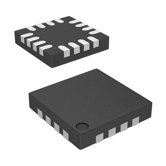
Package Dimensions
unit : mm
3318
SIDE VIEW
TOP VIEW
BOTTOM VIEW
(0.13)
(0.125)
2.6
16
0.4
2.6
(C0.116)
2
1
0.5
LASER MARKED
INDEX
(0.55)
0.25
(0.035)
0.8
SIDE VIEW
SANYO : VCT16
No.A0183-2/10
�LV5213LP
Block Diagram
Note 1: The TEST pin must be tied to ground.
Serial Data Map
Register address
A7
A6
A5
A4
A3
Data
A2
A1
A0
0
0
0
0
0
0
0
1
0
0
0
0
0
0
1
0
0
0
0
0
0
0
1
1
D7
D6
D5
×
×
RSW
0
0
0
×
×
GSW
0
0
0
×
×
BSW
0
0
0
D4
D3
D2
D1
D0
0
0
0
0
0
0
R[4:0]
0
0
0
0
0
G[4:0]
0
B[4:0]
0
0
0
Upper row: Register name, Lower row: default value
No.A0183-3/10
�LV5213LP
Serial Data Mode Settings
R mode
Register address
0
0
0
0
0
Data
0
0
1
D1
D0
0
0
D5
D4
D3
D2
D1
D0
RLED output setting
D5
RSW
0
OFF (Default)
1
ON
RLED current setting
D4
D3
D2
Current [mA]
0
0
0
0
0
0.544 (Default)
0
0
0
0
1
0.679
0
0
0
1
0
0.815
0
0
0
1
1
0.950
0
0
1
0
0
1.085
0
0
1
0
1
1.220
0
0
1
1
0
1.356
0
0
1
1
1
1.491
0
1
0
0
0
1.626
0
1
0
0
1
1.761
0
1
0
1
0
1.897
0
1
0
1
1
2.032
0
1
1
0
0
2.167
0
1
1
0
1
2.302
0
1
1
1
0
2.438
0
1
1
1
1
2.573
1
0
0
0
0
2.708
1
0
0
0
1
2.843
1
0
0
1
0
2.979
1
0
0
1
1
3.114
1
0
1
0
0
3.249
1
0
1
0
1
3.384
1
0
1
1
0
3.520
1
0
1
1
1
3.655
1
1
0
0
0
3.790
1
1
0
0
1
3.925
1
1
0
1
0
4.061
1
1
0
1
1
4.196
1
1
1
0
0
4.331
1
1
1
0
1
4.466
1
1
1
1
0
4.602
1
1
1
1
1
4.737
No.A0183-4/10
�LV5213LP
G mode
Register address
0
0
0
0
0
Data
0
1
0
D1
D0
0
0
D5
D4
D3
D2
D1
D0
GLED output setting
D5
GSW
0
OFF (Default)
1
ON
GLED current setting
D4
D3
D2
Current [mA]
0
0
0
0
0
0.544 (Default)
0
0
0
0
1
0.679
0
0
0
1
0
0.815
0
0
0
1
1
0.950
0
0
1
0
0
1.085
0
0
1
0
1
1.220
0
0
1
1
0
1.356
0
0
1
1
1
1.491
0
1
0
0
0
1.626
0
1
0
0
1
1.761
0
1
0
1
0
1.897
0
1
0
1
1
2.032
0
1
1
0
0
2.167
0
1
1
0
1
2.302
0
1
1
1
0
2.438
0
1
1
1
1
2.573
1
0
0
0
0
2.708
1
0
0
0
1
2.843
1
0
0
1
0
2.979
1
0
0
1
1
3.114
1
0
1
0
0
3.249
1
0
1
0
1
3.384
1
0
1
1
0
3.520
1
0
1
1
1
3.655
1
1
0
0
0
3.790
1
1
0
0
1
3.925
1
1
0
1
0
4.061
1
1
0
1
1
4.196
1
1
1
0
0
4.331
1
1
1
0
1
4.466
1
1
1
1
0
4.602
1
1
1
1
1
4.737
No.A0183-5/10
�LV5213LP
B mode
Register address
0
0
0
0
0
Data
0
1
1
D1
D0
0
0
D5
D4
D3
D2
D1
D0
BLED output setting
D5
BSW
0
OFF (Default)
1
ON
BLED current setting
D4
D3
D2
Current [mA]
0
0
0
0
0
0.544 (Default)
0
0
0
0
1
0.679
0
0
0
1
0
0.815
0
0
0
1
1
0.950
0
0
1
0
0
1.085
0
0
1
0
1
1.220
0
0
1
1
0
1.356
0
0
1
1
1
1.491
0
1
0
0
0
1.626
0
1
0
0
1
1.761
0
1
0
1
0
1.897
0
1
0
1
1
2.032
0
1
1
0
0
2.167
0
1
1
0
1
2.302
0
1
1
1
0
2.438
0
1
1
1
1
2.573
1
0
0
0
0
2.708
1
0
0
0
1
2.843
1
0
0
1
0
2.979
1
0
0
1
1
3.114
1
0
1
0
0
3.249
1
0
1
0
1
3.384
1
0
1
1
0
3.520
1
0
1
1
1
3.655
1
1
0
0
0
3.790
1
1
0
0
1
3.925
1
1
0
1
0
4.061
1
1
0
1
1
4.196
1
1
1
0
0
4.331
1
1
1
0
1
4.466
1
1
1
1
0
4.602
1
1
1
1
1
4.737
No.A0183-6/10
�LV5213LP
Pin Functions
Pin No.
Pin
1
TEST
Test signal input. This pin must be connected to ground.
2
GND
Ground
3
RT
4
BON
External blue LED control input
5
GON
External green LED control input
6
RON
External red LED control input
7
VCC
8
SDATA
9
SCLK
10
CS
11
STBY2
Function
Reference current setting resistor connection
Circuit system power supply
Serial data signal input
Serial clock signal input
Chip select
Standby mode 2 control
Control system (RON, GON, BON, SDATA, SCLK, and CS pins) power supply
12
VDD
13
STBY1
Standby mode 1 control
14
RLED
Red LED driver output
15
GLED
Green LED driver output
16
BLED
Blue LED driver output
No.A0183-7/10
�LV5213LP
Serial Data Transfer Timing Conditions
Parameter
Symbol
Conditions
min
typ
max
unit
Cycle time
tcy1
SCLK clock period
330
nS
Data setup time
ts0
The CS setup time from the SLCK rising edge
150
nS
ts1
The SDATA setup time from the SLCK rising edge
100
nS
Data hold time
th0
The CS hold time from the SLCK falling edge
300
nS
th1
The SDATA hold time from the SCLK rising edge
100
nS
nS
Pulse width
tw1L
SCLK low period pulse width
150
tw1H
SCLK high period pulse width
150
nS
tw2L
CS low period pulse width
1.0
μS
Data length:
Clock frequency:
16bits
Up to 2MHz
After 16 clock cycles have been input with CS at the high level, SDATA is acquired on the fall of CS.
Note: SDATA will not be acquired if 15 or fewer clock cycles were input during the CS high-level period. If 17 or more
clock cycles are input, the SDATA for the first 16 cycles are acquired and the SDATA following those 16 cycles is
ignored.
Power Supply Application
1. Either bring up VCC and VDD at the same time, or bring up VCC first then VDD.
2. Then, set the serial data. (After the serial data has been set, a period of about 2µs is required as the startup time for
the IC internal circuits.)
3. Finally, clear the STBY pin states.
No.A0183-8/10
�LV5213LP
Pin Descriptions and Equivalent Circuits
Pin No.
Symbol
Equivalent circuit
Description
4
BON
Control inputs for the three external colored LEDs
5
GON
When an RSW, GSW, or BSW bit in the serial
6
RON
data is set to 1, the corresponding LED will be on
when the voltage applied to the corresponding
pin is high, and off when the voltage applied is
low.
8
SDATA
9
SCLK
10
CS
3
RT
Serial data system inputs
Reference current setting resistor connection
A reference current is created by connecting an
external resistor between this pin and ground.
The pin voltage is roughly 1.2V. The LED driver
current can be changed by changing this current
value.
14
RLED
Driver outputs for the three color LEDs
15
GLED
Feedback is applied to control the current flowing
16
BLED
in the output transistors to be the set value. Each
of the driver output current levels can be set
independently with the serial data.
Continued on next page.
No.A0183-9/10
�LV5213LP
Continued from preceding page.
Pin No.
Symbol
1
TEST
Equivalent circuit
Description
Test signal input
This pin must be tied to ground.
11
STBY2
Standby mode pins
13
STBY1
The LV5213LP goes to standby mode when both
the STBY1 and STBY2 pins are at the low level.
7
VCC
Circuit system power supply
12
VDD
Control system (serial data inputs and "ON"
3
GND
inputs) power supply
Ground
ON Semiconductor and the ON logo are registered trademarks of Semiconductor Components Industries, LLC (SCILLC). SCILLC owns the rights to a number
of patents, trademarks, copyrights, trade secrets, and other intellectual property. A listing of SCILLC’s product/patent coverage may be accessed at
www.onsemi.com/site/pdf/Patent-Marking.pdf. SCILLC reserves the right to make changes without further notice to any products herein. SCILLC makes no
warranty, representation or guarantee regarding the suitability of its products for any particular purpose, nor does SCILLC assume any liability arising out of the
application or use of any product or circuit, and specifically disclaims any and all liability, including without limitation special, consequential or incidental
damages. “Typical” parameters which may be provided in SCILLC data sheets and/or specifications can and do vary in different applications and actual
performance may vary over time. All operating parameters, including “Typicals” must be validated for each customer application by customer’s technical
experts. SCILLC does not convey any license under its patent rights nor the rights of others. SCILLC products are not designed, intended, or authorized for use
as components in systems intended for surgical implant into the body, or other applications intended to support or sustain life, or for any other application in
which the failure of the SCILLC product could create a situation where personal injury or death may occur. Should Buyer purchase or use SCILLC products for
any such unintended or unauthorized application, Buyer shall indemnify and hold SCILLC and its officers, employees, subsidiaries, affiliates, and distributors
harmless against all claims, costs, damages, and expenses, and reasonable attorney fees arising out of, directly or indirectly, any claim of personal injury or
death associated with such unintended or unauthorized use, even if such claim alleges that SCILLC was negligent regarding the design or manufacture of the
part. SCILLC is an Equal Opportunity/Affirmative Action Employer. This literature is subject to all applicable copyright laws and is not for resale in any manner.
PS No.A0183-10/10
�