IS32LT3128A
TRIPLE CHANNEL LINEAR LED DRIVER WITH FADE ON/OFF AND PWM DIMMING
June 2019
GENERAL DESCRIPTION
FEATURES
The IS32LT3128A is a programmable triple channel
linear current regulator; two channels of up to 150mA
each for LED lighting and a single channel of up to
30mA for illuminating switches. The device operates
as a fully configurable theatrical dimming LED driver;
no microcontroller is required. External resistors will
program the current levels as well as the LED fade
ON/OFF ramp rate. Additional configuration such as
PWM source (internal or external), polarity (positive or
negative) and switch type (momentary contact or
latched) are selectable via the MODE1/2 pins.
An integrated debounce and latch circuit on the
channel enable pin (EN1/2) is enabled when the
device is configured for a momentary contact switch
interface. The other option is to configure the EN pins
to accept a static level signal for operation with latched
switches. A VCC level PWM dimming signal can be
connected to the PWM input pin to directly drive both
LED
channels.
If
configured
for
Internal-PWM-Dimming mode, the integrated PWM
source will be triggered by a PWM pin voltage level.
This enables LED dimming without the need for an
external PWM input. The PWM input have a higher
priority and will override the EN inputs. See Figure
60~66 for the details.
The device integrates a 63 step fade ON/OFF
algorithm (Gamma correction) which causes the output
LED brightness to gradually ramp up to the full source
value after the EN1/2 or PWM (when configured for
Internal-PWM-Dimming mode) pins are triggered. The
same controller causes the LED brightness to
gradually ramp down to zero if the EN1/2 or PWM
(when configured for Internal-PWM-Dimming mode)
pins are triggered while the output channel is ON. The
fade ramp can be interrupted mid-cycle before
completion of the ramp cycle.
The IS32LT3128A is targeted at the automotive market
with end applications to include map and dome lighting
as well as exterior accent lighting. For 12V automotive
applications the low dropout driver can support 1 to 3
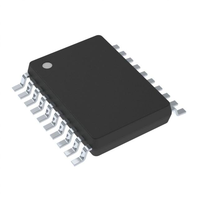
LEDs per channel. It is offered in a small thermally
enhanced eTSSOP-20 package.
Lumissil Microsystems – www.lumissil.com
Rev.A, 05/06/2019
Operating voltage range, 5V to 42V
Dual channel current sources
- Individual programmable current via a single
external resistor
- Configurable from 20mA to 150mA
Single channel 30mA (Max.) current source for
switch illumination
EN input supports either momentary contact or
latched switch
- Input is debounced and latched
- Lower priority than PWM input
- Gamma corrected Fade ON/OFF algorithm
- Pull down resistors set independent fade ON and
OFF ramp time
Selectable external or internal PWM source
- External PWM directly drives the current source
- Internal 220Hz PWM source with Gamma
corrected algorithm for automatic dimming the
current source
- Support both positive and negative polarity PWM
Fault Protection:
- Fault Reporting
LED strings short
Over temperature thermal shutdown
- ISET pin shorted to GND
- Over temperature current roll off
AEC-Q100 Qualified
Operating temperature range from -40°C ~ +125°C
APPLICATIONS
Automotive Interior:
- Map/Dome light
- Puddle lamp in doors
- Glove box light
- Vanity mirror light
1
�IS32LT3128A
TYPICAL APPLICATION CIRCUIT
VBattery
18
RPWM
10k
PWM
50Hz~300Hz
OUT1
OUT2
10 F
5
PWM
OUT3
19
20
1
CPWM
3.3nF
Backlight LED
2
4
Momentary
Contact
3
12
13
14
RISET1 RISET2 RISET3
6
17
Figure 1
VCC
EN3
EN1
FAULTB
IS32LT3128A
EN2
VIO
ISET1
ISET2
ISET3
POL
MODE1
MODE2
TSET_UP
GND
TSET_DN
7
8
Host
RFAULTB
11
1 F
9
10
15 RTSET_UP
16 RTSET_DN
Typical Application Circuit Configured for Momentary Contact Switch And External PWM Dimming
VBattery
18
RPWM
10k
High or Low
Level
OUT1
OUT2
10 F
5
PWM
OUT3
19
20
1
CPWM
3.3nF
Backlight LED
2
VCC
4
Latched
Switch
3
12
13
14
RISET1 RISET2 RISET3
6
17
Figure 2
VCC
EN3
EN1
FAULTB
IS32LT3128A
EN2
ISET1
ISET2
ISET3
VIO
POL
MODE1
MODE2
TSET_UP
GND
TSET_DN
7
8
Host
RFAULTB
11
1 F
9
10
15 RTSET_UP
16 RTSET_DN
Typical Application Circuit Configured for Latched Switch And Internal PWM Dimming
Note 1: The resistor RPWM is a fixed 10kΩ, do not change value. CPWM is optional to minimize electromagnetic susceptibility.
Lumissil Microsystems – www.lumissil.com
Rev.A, 05/06/2019
2
�IS32LT3128A
PIN CONFIGURATION
Package
Pin Configuration (Top View)
eTSSOP-20
Lumissil Microsystems – www.lumissil.com
Rev.A, 05/06/2019
3
�IS32LT3128A
PIN DESCRIPTION
No.
Pin
Description
1
OUT3
Max 30mA output current source for switch backlight LEDs.
2
EN3
Internally deglitch input pin for control of OUT3 current. Pull high (>VIH) to
enable OUT3 current. Pull low (VIH)
to either EN1 or EN2 will turn on the corresponding OUT1 or OUT2 currents.
Grounding either EN1 or EN2 will turn off the corresponding OUT1 or OUT2
current.
11
POL
Internally deglitched input pin for PWM polarity selection. Connect to VIO for
PWM active high and grounded for PWM active low.
12~14
ISET1~ISET3
Output current setting for OUT1/2/3. Connect a resistor between this pin and
GND to set the maximum output current.
15
TSET_UP
Timing control for the Fade ON feature. Connect a resistor between this pin
and GND to set the Fade ON time. Connect this pin directly to ground to
disable the fade function for instant ON.
16
TSET_DN
Timing control for the Fade OFF feature. Connect a resistor between this pin
and GND to set the Fade OFF time. Connect this pin directly to ground to
disable the fade function for instant OFF.
18
VCC
Power supply input pin.
19,20
OUT1,OUT2
Max. 150mA output current source channels.
Thermal Pad
Connect to GND.
Lumissil Microsystems – www.lumissil.com
Rev.A, 05/06/2019
4
�IS32LT3128A
ORDERING INFORMATION
Automotive Range: -40°C to +125°C
Order Part No.
Package
QTY/Reel
IS32LT3128A-ZLA3-TR
eTSSOP-20, Lead-free
2500
Copyright © 2019 Lumissil Microsystems. All rights reserved. Lumissil Microsystems reserves the right to make changes to this specification and its
products at any time without notice. Lumissil Microsystems assumes no liability arising out of the application or use of any information, products or
services described herein. Customers are advised to obtain the latest version of this device specification before relying on any published information and
before placing orders for products.
Lumissil Microsystems does not recommend the use of any of its products in life support applications where the failure or malfunction of the product can
reasonably be expected to cause failure of the life support system or to significantly affect its safety or effectiveness. Products are not authorized for use in
such applications unless Lumissil Microsystems receives written assurance to its satisfaction, that:
a.) the risk of injury or damage has been minimized;
b.) the user assume all such risks; and
c.) potential liability of Lumissil Microsystems is adequately protected under the circumstances
Lumissil Microsystems – www.lumissil.com
Rev.A, 05/06/2019
5
�IS32LT3128A
ABSOLUTE MAXIMUM RATINGS (NOTE 2)
VCC, OUT1/2/3, PWM, EN1/2/3
VIO, POL, MODE1/2, ISET1/2/3, TSET_UP, TSET_DN, FAULTB
Ambient operating temperature, TA=TJ
Maximum continuous junction temperature, TJ(MAX)
Storage temperature range, TSTG
Package thermal resistance, junction to ambient (4 layer standard test
PCB based on JESD 51-2A), θJA
Package thermal resistance, junction to thermal PAD (4 layer standard
test PCB based on JESD 51-8), θJP
Maximum power dissipation, PDMAX
ESD (HBM)
ESD (CDM)
-0.3V ~ +45V
-0.3V ~ +7.0V
-40°C ~ +125°C
150°C
-65°C ~ +150°C
34°C/W
14.46°C/W
2.94W
±2kV
±750V
Note 2: Stresses beyond those listed under “Absolute Maximum Ratings” may cause permanent damage to the device. These are stress
ratings only and functional operation of the device at these or any other condition beyond those indicated in the operational sections of the
specifications is not implied. Exposure to absolute maximum rating conditions for extended periods may affect device reliability.
ELECTRICAL CHARACTERISTICS
TJ = -40°C ~ +125°C, VCC=12V, refer to each condition description. Typical values are at TJ = 25°C.
Symbol
Parameter
VCC
Supply voltage range
VHR
Minimum headroom
voltage
Condition
tON
IOUT_LIM
IOUT
EOUT
EIOUTM
tSL
Quiescent supply
current
Typ.
5
Max. Unit
42
VCC -VOUT1/2, IOUT1/2= -150mA (Note 3)
900
VCC -VOUT1/2, IOUT1/2= -100mA (Note 3)
700
VCC -VOUT3, IOUT3= -30mA (Note 3)
900
OUT1/2/3 output current are all disabled
ICC
Min.
0.1
0.31
1
mV
mA
RISET1= RISET2 =RISET3=15kΩ, OUT1/2/3 output
current are all enabled by ENx, but OUT1/2/3 are
all floating
5.5
mA
VCC=4.2V, OUT1/2 output current are all are
enabled by EN1/2 (only for EN Low Pulse Mode),
EN3 floating
0.25
mA
Startup time
VCC> 6V to IOUT
IS32LT3128A-ZLA3-TR 价格&库存
很抱歉,暂时无法提供与“IS32LT3128A-ZLA3-TR”相匹配的价格&库存,您可以联系我们找货
免费人工找货- 国内价格 香港价格
- 1+16.957811+2.12104
- 10+12.4576310+1.55817
- 25+11.3371425+1.41802
- 100+10.10590100+1.26402
- 250+9.51944250+1.19067
- 500+9.16582500+1.14644
- 1000+8.874871000+1.11005
- 国内价格 香港价格
- 2500+8.567492500+1.07160


 工商网监
湘ICP备2023018690号
工商网监
湘ICP备2023018690号
