Ordering number : ENA0680B
Bi-CMOS LSI
LV5215LF
4ch LED Driver
Overview
The LV5215LF is an LED driver IC for use in cell phones.
Features
• Four main LED driver circuits
• Supports two LED current modes
• Miniature package
• Thermal shutdown function
Specifications
Maximum Ratings at Ta = 25°C
Parameter
Symbol
Maximum supply voltage
VCC max
Maximum input voltage 1
Conditions
Ratings
Unit
VCC
6
V
V1 max
MLED1, MLED2, MLED3, MLED4
6
V
Maximum output current
IO max
ILED
25
mA
Allowable power dissipation
Pd max
Mounted on a circuit board.*
Operating temperature
Storage temperature
* Specified circuit board :
40×50×0.8mm3
0.41
W
Topr
-30 to +75
°C
Tstg
-40 to +125
°C
: glass epoxy four-layer
Recommended Operating Conditions at Ta = 25°C
Parameter
Supply voltage 1
Symbol
VBAT
Conditions
Ratings
Unit
3.0 to 4.5
V
Any and all SANYO Semiconductor Co.,Ltd. products described or contained herein are, with regard to
"standard application", intended for the use as general electronics equipment (home appliances, AV equipment,
communication device, office equipment, industrial equipment etc.). The products mentioned herein shall not be
intended for use for any "special application" (medical equipment whose purpose is to sustain life, aerospace
instrument, nuclear control device, burning appliances, transportation machine, traffic signal system, safety
equipment etc.) that shall require extremely high level of reliability and can directly threaten human lives in case
of failure or malfunction of the product or may cause harm to human bodies, nor shall they grant any guarantee
thereof. If you should intend to use our products for applications outside the standard applications of our
customer who is considering such use and/or outside the scope of our intended standard applications, please
consult with us prior to the intended use. If there is no consultation or inquiry before the intended use, our
customer shall be solely responsible for the use.
Specifications of any and all SANYO Semiconductor Co.,Ltd. products described or contained herein stipulate
the performance, characteristics, and functions of the described products in the independent state, and are not
guarantees of the performance, characteristics, and functions of the described products as mounted in the
customer' s products or equipment. To verify symptoms and states that cannot be evaluated in an independent
device, the customer should always evaluate and test devices mounted in the customer' s products or
equipment.
O0610 SY/20707 MS PC 20070118-S00001 No.A0680-1/5
�LV5215LF
Electrical Characteristics at Unless otherwise specified Ta = 25°C, VBAT = 3.7V
Parameter
Symbol
Ratings
Conditions
min
typ
Unit
max
[Analog Block] Current drain
Current drain 1
ICC1
VBAT + VDD current drain. CTL: low
0
5
μA
Current drain 2
ICC2
CTL : H
3
5
mA
LED Driver Block at R1 = 110kΩ, R2 = 11kΩ
LED current 1
ILED1
VO = 0.5V *1
1
2
3
mA
LED current 2
ILED2
VO = 0.5V *1
18
20
22
mA
Control Circuit Block
High level 1
VINH1
High-level input *2
1.5
VBAT
V
Low level 1
VINL1
Low-level input *2
0
0.3
V
Switch on state resistance
RON
SWI pin : VBAT
Ω
200
*1 : ILED will have a value about 200 times that of the current (IRT) flowing in the current setting resistor (RT).
*2 : The IC operates when CTL is high, and stops when CTL is low.
Package Dimensions
unit : mm (typ)
3335
Pd max -- Ta
TOP VIEW
Allowable power dissipation, Pd max -- W
0.6
BOTTOM VIEW
SIDE VIEW
Exposed Die-Pad
Do Not Connect
2.0
1
(1.0)
0.25
2.0
(1.0)
12
2
2
1
0.5 (0.5)
0.25
0.0NOM
0.5
0.41
Mounted on a
circuit board
0.41
0.4
0.3
0.21
0.2
0.1
0
-40
(0.8)
0.85MAX
SIDE VIEW
Specified circuit board : 40×50×0.8mm3
glass epoxy four-layer
-20
0
20
40
60
80
100
Ambient temperature, Ta -- °C
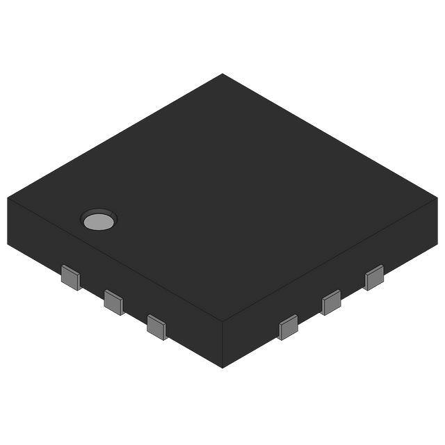
SANYO : VQFN12(2.0X2.0)
RT
SWO
SWI
Pin Assignment
9
8
7
GND 10
6 NC
VCC 11
5 CTL
4 GND
1
2
3
MLED3
MLED2
MLED1
MLED4 12
Top view
No.A0680-2/5
�LV5215LF
Block Diagram
VBAT
ILED
VCC1
MLED1
MLED2
MLED3
MLED4
VCC
LED DRIVER
IREF
SWI
SWO
CTL
GND
IRT
R2
11kΩ
RT
IF
R1
110kΩ
ILED = 200 × IRT
No.A0680-3/5
�LV5215LF
Pin Equivalent Circuit
Pin No.
Pin
Description
1
MLED3
LED driver pin.
2
MLED2
Feedback is applied so that the current
3
MLED1
flowing in the output transistor becomes
12
MLED4
the set current value.
Equivalent Circuit
VCC
MLED*
10Ω
GND
11
VCC
Power supply.
VCC
GND
5
CTL
The circuits operate when CTL is high.
The circuits stop when CTL is low.
VCC
1MΩ
CTL
18kΩ
GND
9
RT
Reference current setting resistor
connection.
VCC
The reference current is created by
30pF
connecting an external resistor to ground.
The pin voltage is about 1.0 V.
The LED driver current value can be
3.5kΩ
RT
changed by changing this current value.
10kΩ
GND
7
SWI
Current adjustment.
8
SWO
The output current can be adjusted using
VCC
the SWO pin sink current.
SWO
SWI
18kΩ
GND
No.A0680-4/5
�LV5215LF
SANYO Semiconductor Co.,Ltd. assumes no responsibility for equipment failures that result from using
products at values that exceed, even momentarily, rated values (such as maximum ratings, operating condition
ranges, or other parameters) listed in products specifications of any and all SANYO Semiconductor Co.,Ltd.
products described or contained herein.
SANYO Semiconductor Co.,Ltd. strives to supply high-quality high-reliability products, however, any and all
semiconductor products fail or malfunction with some probability. It is possible that these probabilistic failures or
malfunction could give rise to accidents or events that could endanger human lives, trouble that could give rise
to smoke or fire, or accidents that could cause damage to other property. When designing equipment, adopt
safety measures so that these kinds of accidents or events cannot occur. Such measures include but are not
limited to protective circuits and error prevention circuits for safe design, redundant design, and structural
design.
In the event that any or all SANYO Semiconductor Co.,Ltd. products described or contained herein are
controlled under any of applicable local export control laws and regulations, such products may require the
export license from the authorities concerned in accordance with the above law.
No part of this publication may be reproduced or transmitted in any form or by any means, electronic or
mechanical, including photocopying and recording, or any information storage or retrieval system, or otherwise,
without the prior written consent of SANYO Semiconductor Co.,Ltd.
Any and all information described or contained herein are subject to change without notice due to
product/technology improvement, etc. When designing equipment, refer to the "Delivery Specification" for the
SANYO Semiconductor Co.,Ltd. product that you intend to use.
Information (including circuit diagrams and circuit parameters) herein is for example only; it is not guaranteed
for volume production.
Upon using the technical information or products described herein, neither warranty nor license shall be granted
with regard to intellectual property rights or any other rights of SANYO Semiconductor Co.,Ltd. or any third
party. SANYO Semiconductor Co.,Ltd. shall not be liable for any claim or suits with regard to a third party's
intellctual property rights which has resulted from the use of the technical information and products mentioned
above.
This catalog provides information as of October, 2010. Specifications and information herein are subject
to change without notice.
PS No.A0649-5/5
�