TS19451
AC/DC WLED Driver with Internal MOSFET
Universal Switch Mode
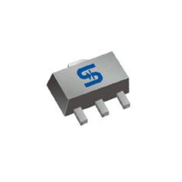
SOT-89
Pin Definition:
1. Drain
2. GND
3. VDD
General Description
en
de
d
The TS19451 is a PWM high efficiency LED driver control IC. It allows efficient operation of LED strings from
voltage source ranging up to 400VDC. It includes an internal high voltage switching MOSFET controlled with fixed
off-time of approximately 10.5µS.
The LED string is driven at constant current, thus providing constant light output and enhanced reliability. The
output current is internally fixed at 50mA. The peak current control scheme provides good regulation of the output
current throughout the universal AC line voltage range of 85~264VAC or DC input voltage of 20~400V
Typical Application Circuit
●
Constant output current at 50mA
●
Universal 85~264VAC operation
●
Fixed off-time buck converter
●
Internal 475V power MOSFET
Application
●
Decorating LED lighting
●
Lower power lighting fixtures
●
Back light of flat panel displays
eco
Ordering Information
mm
Features
Part No.
Package
Packing
TS19451CY RMG
SOT-89
1Kpcs / 7” Reel
tR
Note: “G” denotes for Halogen Free
Absolute Maximum Rating
Parameter
Symbol
Limit
Unit
VIN to GND
~ +475
V
Supply Current
IDD
5
mA
Power Dissipation @ TA=25ºC
PD
1300
mW
Operating Ambient Temperature
TOPR
-40 to +85
ºC
Storage Temperature Range
TSTG
-65 to +150
o
-40 to +150
o
No
Input Voltage Range
Junction Temperature Range
TJ
Thermal Resistance – Junction to Ambient
RθJA
128
C
C
o
C/W
Note: Stresses beyond those listed under ”Absolute Maximum Ratings” may cause permanent damage to the
device. These are stress rating only, and functional operation of the device at these or any other conditions beyond
those indicated in the operational sections of the specifications is not implied. Exposure to absolute maximum
rating conditions for extended periods may affect device reliability.
1/7
Version: B11
�TS19451
AC/DC WLED Driver with Internal MOSFET
Universal Switch Mode
Electrical Specifications (Ta = 25oC, VDRAIN= 50V, unless otherwise noted)
Function Parameter
Symbol
Test Conditions
Min
Typ
Max
Units
VDD
--
7.5
--
V
Drain Supply Voltage
VDRAIN
--
20
--
V
Undervoltage Lockout Threshold
UVLO
4.0
--
--
V
Undervoltage Lockout Hysteresis
∆UVLO
--
200
--
mV
--
200
350
µA
Internal Regulator
Supply Current
IDD
VDD(EXT)=8.5V, VDRAIN=40V
d
Internally Regulated Voltage
Breakdown Voltage
VBR
RDSON
IDRAIN=50mA
Output Capacitance
CDRAIN
VDRAIN=400V
MOSFET Saturation current
ISAT
Current Sense Comparator
ITH
mm
Threshold Current
--
--
V
--
--
210
Ω
--
1.0
5.0
pF
100
150
--
mA
49
--
63
mA
en
On Resistance
475
de
Output (Drain)
Leading edge Blanking delay
TBLANK
200
300
400
nS
Minimum Turn On-Time
TON(MIN)
--
--
650
nS
TOFF
8
10.5
13
µS
Off-Time Generator
Turn On-Time
No
tR
Block Diagram
e co
Note 1: The specification which apply over the full operating ambient temperature range of -40ºC
很抱歉,暂时无法提供与“TS19451CY RMG”相匹配的价格&库存,您可以联系我们找货
免费人工找货