Advanced Science And Novel Technology Company, Inc.
2790 Skypark Drive Suite 112, Torrance, CA 90505
Offices: 310-530-9400 / Fax: 310-530-9402
www.adsantec.com
ASNT1140-KMA
DC-to-50Gbps Programmable DDR Multiplexer 16:1 / Serializer
76 vcc
77 d05p
78 d05n
79 vcc
80 d06p
81 d06n
82 vcc
83 d07p
84 d07n
85 vcc
86 d08p
87 d08n
88 vcc
89 d09p
90 d09n
91 vcc
92 d10p
93 d10n
94 vcc
95 d11p
96 d11n
97 vcc
98 d12p
99 d12n
100 vcc
Rev. 1.8.2
vee 75
vecl 74
d04n 73
d04p 72
vcc 71
d03n 70
d03p 69
vcc 68
d02n 67
d02p 66
vcc 65
d01n 64
d01p 63
vcc 62
d00n 61
d00p 60
bitorder 59
vee 58
phs1 57
phs2 56
vcc 55
nc 54
nc 53
vee 52
vee 51
Programmable digital serializer 16-to-1
Supports data rates from DC to 50Gb/s in DDR clocking mode
Programmable LVDS/CML/ECL input data buffers
CML input clock buffer
Switchable forwarded DDR clock output phase-aligned with output data
LVDS output full-rate sampling clock with a selectable phase to synchronize input data
External reset for synchronization of multiple devices
Single +3.3V power supply
Industrial temperature range
Power consumption of 1520mW at maximum speed
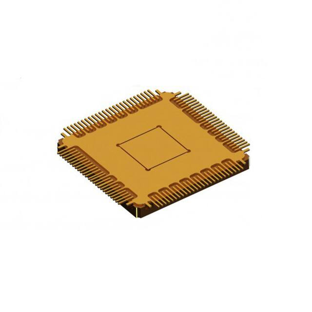
Custom 100-pin CQFP package (13mm x 13mm)
ASNT 1140
vee 50
clop 49
clon 48
ampadj 47
rstp 46
rstn 45
vcc 44
nc 43
nc 42
vcc 41
qp 40
qn 39
vcc 38
cdcadj 37
vee 36
vcc 35
c2op 34
c2on 33
vcc 32
vtrm 31
vtrm 30
vcc 29
c2ip 28
c2in 27
vcc 26
1 vee
2 vecl
3 d13p
4 d13n
5 vcc
6 d14p
7 d14n
8 vcc
9 d15p
10 d15n
11 vcc
12 nc
13 nc
14 offecl
15 vee
16 nc
17 vee
18 offcho
19 nc
20 nc
21 nc
22 cdccn
23 vee
24 cdccp
25 vcc
1
May 2020
�Advanced Science And Novel Technology Company, Inc.
2790 Skypark Drive Suite 112, Torrance, CA 90505
Offices: 310-530-9400 / Fax: 310-530-9402
www.adsantec.com
DESCRIPTION
bitorder
d00p/d00n
d15p/d15n
offecl
vecl
rstp/rstn
vtrm
cdccp
cdccn
cdcadj
c2ip/c2in
DIB
x16
16
Data
OB
MUX
16:1
C16
CLK
Proc
HS
CIB
LVDS
COB
qp/qn
clop/clon
phs1
phs2
/8
C2
ampadj
HS
COB
offcho
c2op/c2on
Fig. 1. Functional Block Diagram
ASNT1140-KMA is a high-speed DDR (dual data rate) digital 16-to-1 multiplexer (MUX) / serializer.
The IC shown in Fig. 1 functions seamlessly over the specified range of data rates (fbit).
The main function of the IC is to multiplex 16 parallel data channels running at a bit rate of fbit/16 into a
high-speed serial bit stream running at fbit. It provides a high-speed output data channel for point-to-point
data transmission over a controlled impedance media of 50Ohm. The transmission media can be a printed
circuit board or copper coaxial cables. The functional distance of the data transfer is dependent upon the
attenuation characteristics of the transportation media and the degree of noise coupling to the signaling
environment.
During normal operation, the serializer’s data input buffer (DIBx16) accepts external 16-bit wide parallel
data words d00p/d00n-d15p/d15n through 16 differential LVDS inputs and delivers them to the
multiplexer’s core (MUX16:1) for serialization. A half-rate CML clock (a full-rate clock divided by 2)
must be provided by an external source to the inputs c2ip/c2in of the high-speed clock input buffer (HS
CIB) where it is routed to both the high-speed clock output buffer (HS COB) and the internal divider-by-8
(/8). The high-speed CML clock input buffer provides on-chip 50Ohm termination and is designed to be
driven by devices with 50Ohm source impedance. The duty cycle of the internal clock c2 can be adjusted
either through a single ended control pin cdcadj or through a dual control port cdccp/cdccn. The clock
input buffer uses a separate positive supply vtrm for additional common mode voltage adjustment.
The divider provides signaling for MUX16:1 and produces a divided-by-16 full-rate sampling clock C16
for the low-speed LVDS-compliant clock output buffer (LVDS COB). The divider can be preset to a
certain initial state using external CML signals rstp/rstn.
The phase of the low-speed output sampling clock clop/clon can be modified in 90° increments by
utilizing pins phs1 and phs2 and the clock processing block (CLK Proc). By utilizing the pin bitorder,
the serializer can designate either d00p/d00n or d15p/d15n as the MSB (most significant bit that is
delivered first to the serial interface), thus simplifying the interface between the multiplexer and a
preceding device.
Rev. 1.8.2
2
May 2020
�Advanced Science And Novel Technology Company, Inc.
2790 Skypark Drive Suite 112, Torrance, CA 90505
Offices: 310-530-9400 / Fax: 310-530-9402
www.adsantec.com
The serialized words are transmitted as a differential signal qp/qn by a CML output buffer (Data OB). A
DDR mode forwarded CML clock c2op/c2on is transmitted by HS COB in parallel with the high-speed
data. The clock and data outputs are well phase matched to each other resulting in very little relative skew
over the operating temperature range of the device. Both output stages are back terminated with on-chip
50Ohm resistors. An example of a differential output eye at 28Gb/s is shown in Fig. 2.
Fig. 2. 28Gb/s Output Eye
The chip uses a single +3.3V power supply and is characterized for operation from −25°C to 125°C of
junction temperature.
DIBx16
The Data Input Buffer (DIB) is a proprietary universal input buffer (UIB) that can run at a frequency up to
2.5GHz. The input termination impedance is controlled by 3.3V CMOS signal offecl and is set to 100Ohm
differential if offecl = “1” (true LVDS mode, default state) or 50Ohm single-ended to vecl if offecl = “0”
(CML mode). The value of vecl should be equal to vcc in CML mode or vcc-2V in PECL mode. In this
case, the corresponding termination voltage source should be able to both sink and source up to 20mA of
current. Possible input clock application schemes are detailed in Table 1, where Vcm is the commonmode voltage of the clock signal.
Table 1. LS Input Clock Application Schemes
Interface Clock
cep signal
type
type Swing, mV Connection
Vcm, V
LVDS
Diff.
70-to-500
DC
1.2±1.0
(offecl
SE
140-to-900
AC
= “1”)
Threshold
DC
vee-to-vcc
CML or
Diff.
70-to-500
DC
vcc-Swing/2
PECL
AC
(offecl
SE
140-to-900
AC
= “0”)
140-to-900
AC
N/C
Threshold
DC
vcc
Swing, mV
70-to-500
Threshold
140-to-900
70-to-500
Threshold
140-to-900
140-to-900
cen signal
Connection
Vcm, V
DC
1.2±1.0
DC
vee-to-vcc
AC
DC
vcc-Swing/2
AC
Not
connected
DC
vcc
AC
AC
-
As can be seen, UIB is designed to accept differential signals with amplitudes above 60mV peak-to-peak
(p-p), DC common mode voltage variation between negative vee and positive vcc supply rails, and AC
common mode noise with a frequency up to 5MHz and voltage levels ranging from 0 to 2.4V. It can also
receive single-ended signals with amplitudes above 60mVp-p and threshold voltages between vee and
vcc. UIB fully complies with LVDS standards IEEE Std. 1596.3-1996 and ANSI/TIA/EIA-644-1995.
Rev. 1.8.2
3
May 2020
�Advanced Science And Novel Technology Company, Inc.
2790 Skypark Drive Suite 112, Torrance, CA 90505
Offices: 310-530-9400 / Fax: 310-530-9402
www.adsantec.com
HS CIB
The High-Speed Clock Input Buffer (HS CIB) can accept high-speed clock signals at its differential CML
input port c2ip/c2in. It can also accept a single-ended signal with a threshold voltage applied to the
unused pin. HS CIB can handle a wide range of input signal amplitudes. The buffer utilizes on-chip
single-ended 50Ohm termination to vtrm for each input line. This termination voltage can be adjusted
within the range from vcc to vcc-0.8V.
The buffer provides two options for adjustment of its output signal duty cycle. The duty cycle can be
adjusted by changing two control voltages cdccp and cdccn that affect the input signals c2ip and c2in
respectively.
It can also be adjusted using one control voltage cdcadj following the diagram shown in Fig. 3. Here red
lines correspond to the dp input, blue lines correspond to the dn input, solid lines represent typical
conditions while dotted and dashed lines represent slow and fast conditions respectively.
Fig. 3. Duty Cycle Control Diagram
It should be noted that only one control option should be activated at a certain time. Either cdccp/cdccn
or cdcadj pins should be left not connected or AC-terminated with 50Ohm loads. Otherwise, the two
internal control circuits interact and the desired result cannot be achieved.
/8
The Divider-by-8 (/8) includes three divide-by-2 circuits connected in series. The half-speed clock C2 is
routed internally to the first divide-by-2 circuit and outside of the block to MUX16:1. Other divided down
clock signals are formed and routed to MUX16:1 in a similar fashion. C16 is passed on to LVDS COB to
become the output low-speed sampling clock signal clop/clon.
The divider can be preset to a “0” state using external differential CML signals rstp/rstn that have onchip 50Ohm termination to vcc. The reset circuitry can operate at high speed and features internal
retiming by the falling edge of half-rate clock. The desired phase relation between the reset signal and the
input clock c2ip/c2in is illustrated by Fig. 4 and specified in Table 2Error! Reference source not found..
Rev. 1.8.2
4
May 2020
�Advanced Science And Novel Technology Company, Inc.
2790 Skypark Drive Suite 112, Torrance, CA 90505
Offices: 310-530-9400 / Fax: 310-530-9402
www.adsantec.com
Table 2. Input Reset to Input Low-Speed Sampling Clock Phase Delay
Maximum required recovery time, ps Maximum required removal time, ps
-18
33
tremoval
Input
c2ip
trecovery
Input
rstp
Fig. 4. Reset Timing Diagram
MUX16:1
The 16-to-1 Multiplexer (MUX16:1) utilizes a tree-type architecture which latches the incoming data on
the negative edge of the C16 clock signal supplied by /8. The 16-bit wide data word is subsequently
multiplexed and delivered to Data OB as a single serial data stream. The latency of this circuit block is
equal to roughly one period of C16. The output bit order is controlled by the 3.3V CMOS signal bitorder.
The first output serial bit (MSB) corresponds to d00p/d00n when bitorder = “0” (default), or to
d15p/d15n when bitorder = “1”.
Data OB
The Data Output Buffer (Data OB) receives high-speed serial data from MUX16:1 and converts it into a
differential CML output signal qp/qn. Each buffer utilizes internal single-ended 50Ohm loads to vcc and
requires single-ended 50Ohm external termination. The termination resistors can be connected from each
output directly to vcc, or through DC blocks to vee. The amplitude of the output signals can be adjusted
from 0 to its maximum value using the external control voltage ampadj. Higher values of the control
voltage correspond to higher amplitude values as shown in Fig. 5.
Fig. 5. Simulated Amplitude Control Characteristic
Rev. 1.8.2
5
May 2020
�Advanced Science And Novel Technology Company, Inc.
2790 Skypark Drive Suite 112, Torrance, CA 90505
Offices: 310-530-9400 / Fax: 310-530-9402
www.adsantec.com
HS COB
The High Speed Clock Output Buffer (HS COB) utilizes the same termination scheme as Data OB and
can operate at the maximum frequency while producing a full single-ended CML output swing. The
buffer can be enabled or disabled by the external 3.3V CMOS control signal offcho. The logic “0” state
provides a half-rate clock output signal c2op/c2on, while the logic “1” state disables the buffer
completely.
CLK Proc
By utilizing the 3.3V CMOS control pins phs1 and phs2, the phase of the clop/clon signal can be altered
in accordance with Table 3.
Table 3. Output Clock Phase Selection
phs1
phs2
clop/clon phase
vee (default) vee (default)
90°
180°
vee
vcc
270°
vcc
vee
0°
vcc
vcc
LVDS COB
The LVDS Clock Output Buffer (LVDS COB) receives the divided clock C16 and converts it into a
differential output signal clop/clon. The proprietary low-power LVDS output buffer utilizes a special
architecture that ensures operation at high frequencies with a nominal output current of 3.5mA. The buffer
satisfies all the requirements of the IEEE Std. 1596.3-1996 and ANSI/TIA/EIA-644-1995 standards.
Input Timing
Reliable latching of the incoming data dXXp/dXXn requires a certain phase relation between the input
data and the full-rate output sampling clock clop that is specified in Table 4 and illustrated by Fig. 6,
when phs1 = “0” and phs2 = “1”.
Table 4. Input Data to Output Low-Speed Sampling Clock Phase Delay
Maximum required setup time, ps Maximum required hold time, ps
0
90
thold
clop
tsetup
dp/dn
Fig. 6. Input Timing Diagram
Rev. 1.8.2
6
May 2020
�Advanced Science And Novel Technology Company, Inc.
2790 Skypark Drive Suite 112, Torrance, CA 90505
Offices: 310-530-9400 / Fax: 310-530-9402
www.adsantec.com
Output Timing
The phase relation between the output data qp/qn and the half-rate forwarded output clock c2op is
specified in Table 5 and illustrated by Fig. 7.
Table 5. Output Data to Output High-Speed Forwarded Clock Phase Delay
tqc2, ps
Min
3.0
Max
4.6
tqc2
c2op
tqc2
qp/qn
Fig. 7. Output Timing Diagram
ABSOLUTE MAXIMUM RATINGS
Caution: Exceeding the absolute maximum ratings shown in Table 6 may cause damage to this product
and/or lead to reduced reliability. Functional performance is specified over the recommended operating
conditions for power supply and temperature only. AC and DC device characteristics at or beyond the
absolute maximum ratings are not assumed or implied. All min and max voltage limits are referenced to
ground (assumed vee).
Table 6. Absolute Maximum Ratings
Parameter
Supply Voltage (vcc)
Power Consumption
RF Input Voltage Swing (SE)
Case Temperature
Storage Temperature
Operational Humidity
Storage Humidity
Rev. 1.8.2
Min
-40
10
10
7
Max
+3.6
1.6
1.0
+90
+100
98
98
Units
V
W
V
ºC
ºC
%
%
May 2020
�Advanced Science And Novel Technology Company, Inc.
2790 Skypark Drive Suite 112, Torrance, CA 90505
Offices: 310-530-9400 / Fax: 310-530-9402
www.adsantec.com
TERMINAL FUNCTIONS
Supply and Termination Voltages
Name
Description
Pin Number
vcc
Positive power supply (+3.3V) 5, 8, 11, 25, 26, 29, 32, 35, 38, 41, 44, 55, 62,
65, 68, 71, 76, 79, 82, 85, 88, 91, 94, 97, 100
vee
Negative power supply (GND
1, 15, 17, 23, 36, 50, 51, 52, 58, 75
or 0V)
vecl Input termination voltage (vcc
2, 74
for CML, vcc-2V for ECL)
vtrm Termination voltage for clock
30, 31
input duty cycle control
circuit (default – vcc,
minimum – vcc-0.8V)
nc
Not connected
12, 13, 16, 19, 20, 21, 42, 43, 53, 54
TERMINAL
Name
No.
Type
DESCRIPTION
High-Speed I/Os
Differential external clock inputs with internal SE 50Ohm
termination to vcc
Differential forwarded clock outputs. Require external SE
50Ohm termination to vcc. Can be disabled by offcho
Differential data outputs. Require external SE 50Ohm
termination to vcc
Differential reset inputs with internal SE 50Ohm termination to
vcc
Controls
LS input clock and data termination selector (active: low, CML
or PECL depending on vecl connection; default: high, LVDS)
HS COB control (active: high, buffer is disabled; default: low,
half-rate output clock)
Input half-rate clock duty cycle SE control with internal
termination to a resistive divider
Output data amplitude control voltage with internal termination
to a resistive divider
Input half-rate clock duty cycle differential controls with
internal 200Ohm termination to the corresponding clock inputs
Low-speed output sampling clock phase selection (see Table 3)
c2ip
c2in
c2op
c2on
qp
qn
rstp
rstn
28
27
34
33
40
39
46
45
CML
input
CML
output
CML
output
CML
input
offecl
14
offcho
18
cdcadj
37
ampadj
47
cdccp
cdccn
phs1
phs2
bitorder
24
22
57
56
59
CMOS
input
CMOS
input
Analog
Input
Analog
Input
Analog
Inputs
CMOS
input
CMOS Input bit order selection (active: high, d15p/d15n is serialized
input first; default: low, d00p/d00n is serialized first)
Rev. 1.8.2
8
May 2020
�Advanced Science And Novel Technology Company, Inc.
2790 Skypark Drive Suite 112, Torrance, CA 90505
Offices: 310-530-9400 / Fax: 310-530-9402
www.adsantec.com
TERMINAL
Name
No.
Type
clop
clon
d00p
d00n
d01p
d01n
d02p
d02n
d03p
d03n
d04p
d04n
d05p
d05n
d06p
d06n
d07p
d07n
d08p
d08n
d09p
d09n
d10p
d10n
d11p
d11n
d12p
d12n
d13p
d13n
d14p
d14n
d15p
d15n
Rev. 1.8.2
49
48
60
61
63
64
66
67
69
70
72
73
77
78
80
81
83
84
86
87
89
90
92
93
95
96
98
99
3
4
6
7
9
10
DESCRIPTION
Low-Speed I/Os
Output LVDS divided-by-16 full-rate sampling clock outputs
Input
LVDS data inputs
9
May 2020
�Advanced Science And Novel Technology Company, Inc.
2790 Skypark Drive Suite 112, Torrance, CA 90505
Offices: 310-530-9400 / Fax: 310-530-9402
www.adsantec.com
ELECTRICAL CHARACTERISTICS
PARAMETER
TYP MAX
UNIT
COMMENTS
General Parameters
+3.14
+3.3
+3.47
V
±5%
vcc
vcc
vcc -0.8
V
vtrm
0.0
V
External ground
vee
Ivcc
460
mA
Power consumption
1520
mW
Junction temperature
-25
50
125
°C
LS Input Data (d00p/d00n-d15p/d15n)
Maximum Data Rate 3.125
Gbps
Minimum Data Rate
Gbps
Differential Swing
0.06
0.8
V
Peak-to-peak
CM Voltage Level
V
vee
vcc
HS Input Clock (c2ip/c2in)
Maximum Frequency
25
GHz
Minimum Frequency
GHz
Swing (Diff or SE)
0.2
1.0
V
Peak-to-peak
CM Voltage Level
vcc-0.8
vcc
V
Duty Cycle
40
50
60
%
HS Output Data (qp/qn)
Maximum Data Rate
50
Gbps
Minimum Data Rate
Gbps
Logic “1” level
V
vcc
Logic “0” level
vcc-0.05
V
minimum ampadj
vcc-1.0
vcc-1.3
V
maximum ampadj
Rise/fall time
4
12
ps
0.2-0.8 of the amplitude
Jitter
1
2
ps
Peak-to-peak at 32Gb/s
HS Output Forwarded Clock (c2op/c2on)
Maximum Frequency
25
GHz
Minimum Frequency
GHz
Logic “1” level
V
vcc
Logic “0” level
vcc-0.65
V
Rise/fall time
8
17
ps
0.2-0.8 of the amplitude
Duty Cycle
50
%
LS Output Sampling Clock (clop/clon)
Maximum Frequency 3.125
GHz
Minimum Frequency
GHz
Interface
LVDS
Meets the IEEE Std.
CMOS Control Inputs (offecl, bitorder, offcho, phs1, phs2)
Logic “1” level
vcc-0.4
V
Logic “0” level
vee+0.4
V
Rev. 1.8.2
MIN
10
May 2020
�Advanced Science And Novel Technology Company, Inc.
2790 Skypark Drive Suite 112, Torrance, CA 90505
Offices: 310-530-9400 / Fax: 310-530-9402
www.adsantec.com
PARAMETER
MIN
TYP MAX
UNIT
COMMENTS
Analog Control Inputs (ampadj, cdcadj, cdccp/cdccn)
Voltage range
V
vee
vcc
ampadj termination
2.3 / 2.3
KOhm to vee / vcc
cdcadj termination
22 / 5.6
KOhm to vee / vcc
cdccp termination
0.95
KOhm to c2ip
cdccn termination
0.95
KOhm to c2in
PACKAGE INFORMATION
Fig. 8. CQFP 100-Pin Package Drawing (All Dimensions in mm)
Rev. 1.8.2
11
May 2020
�Advanced Science And Novel Technology Company, Inc.
2790 Skypark Drive Suite 112, Torrance, CA 90505
Offices: 310-530-9400 / Fax: 310-530-9402
www.adsantec.com
The chip die is housed in a custom 100-pin CQFP package shown in Fig. 8. The package’s leads will be
trimmed to a length of 1.0mm. After trimming, the package’s leads will be further processed as follows:
1. The lead’s gold plating will be removed per the following sections of J-STD-001D:
3.9.1 Solderability
3.2.2 Solder Purity Maintenance
3.9.2 Solderability Maintenance
3.9.3 Gold Removal
2. The leads will be tinned with Sn63Pb37 solder
The package provides a center heat slug located on its back side to be used for heat dissipation.
ADSANTEC recommends for this section to be soldered to the vcc plain, which is power for a positive
supply.
The part’s identification label is ASNT1140-KMA. The first 8 characters of the name before the dash
identify the bare die including general circuit family, fabrication technology, specific circuit type, and part
version while the 3 characters after the dash represent the package’s manufacturer, type, and pin out
count.
This device complies with the Restriction of Hazardous Substances (RoHS) per 2011/65/EU for all ten
substances.
REVISION HISTORY
Revision
1.8.2
1.7.2
1.7.1
1.6.1
Date
05-2020
07-2019
01-2019
07-2015
1.5.1
07-2015
1.4.1
05-2015
1.3.1
1.2.1
03-2015
03-2015
1.1.1
1.0.1
03-2015
03-2015
1.0.0
11-2014
Rev. 1.8.2
Changes
Updated Package Information
Updated Letterhead
Added differential output eye
Corrected pinout diagram (pins 52 and 53)
Corrected Terminal Functions
Updated frequency of operation
Updated Electrical characteristics table
Revised package information section
Updated format
Updated Data OB section
Corrected block diagram
Corrected description of vtrm function
Added vtrm range
Corrected Pin out Diagram
Corrected power consumption based on measurements
Corrected description of timing parameters
Preliminary release
12
May 2020
�


 工商网监
湘ICP备2023018690号
工商网监
湘ICP备2023018690号
