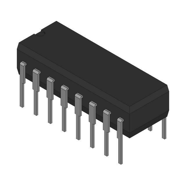
HIN232A
®
Data Sheet
March 13, 2006
High Speed +5V Powered RS-232
Transmitters/Receivers
FN4316.12
Features
• Meets All RS-232E and V.28 Specifications
The HIN232A high-speed RS-232 transmitter/receiver
interface circuit meets all ElA high-speed RS-232E and V.28
specifications, and is particularly suited for those
applications where ±12V is not available. They require a
single +5V power supply and feature onboard charge pump
voltage converters which generate +10V and -10V supplies
from the 5V supply.
• Requires Only 0.1µF or Greater External Capacitors
• High Data Rate. . . . . . . . . . . . . . . . . . . . . . . . . . 230kbit/s
• Requires Only Single +5V Power Supply
• Onboard Voltage Doubler/Inverter
• Low Power Consumption (Typ) . . . . . . . . . . . . . . . . . 5mA
The drivers feature true TTL/CMOS input compatibility, slew
rate-limited output, and 300Ω power-off source impedance.
The receivers can handle up to ±30V input, and have a 3kΩ
to 7kΩ input impedance. The receivers also feature
hysteresis to greatly improve noise rejection.
• Multiple Drivers
- ±10V Output Swing for +5V lnput
- 300Ω Power-Off Source Impedance
- Output Current Limiting
- TTL/CMOS Compatible
Ordering Information
• Multiple Receivers
- ±30V Input Voltage Range
- 3kΩ to 7kΩ Input Impedance
- 0.5V Hysteresis to Improve Noise Rejection
PART NO.
PART
MARKING
TEMP.
RANGE
(oC)
PACKAGE
PKG.
DWG.
#
HIN232ACB
232ACB
0 to 70
16 Ld SOIC
M16.3
HIN232ACB-T
232ACB
0 to 70
16 Ld SOIC
Tape and Reel
M16.3
HIN232ACBZ
(See Note)
232ACBZ
0 to 70
16 Ld SOIC
(Pb-free)
M16.3
HIN232ACBZ-T
(See Note)
232ACBZ
0 to 70
16 Ld SOIC
Tape and Reel
(Pb-free)
M16.3
HIN232ACBN
232ACBN
0 to 70
16 Ld SOIC (N) M16.15
HIN232ACBN-T
232ACBN
0 to 70
16 Ld SOIC (N) M16.15
Tape and Reel
HIN232ACBNZ
(See Note)
232ACBNZ
0 to 70
16 Ld SOIC (N) M16.15
(Pb-free)
HIN232ACBNZ-T 232ACBNZ
(See Note)
0 to 70
16 Ld SOIC (N) M16.15
Tape and Reel
(Pb-free)
HIN232ACP
HIN232ACP
0 to 70
16 Ld PDIP
E16.3
HIN232ACPZ
(See Note)
232ACPZ
0 to 70
16 Ld PDIP*
(Pb-free)
E16.3
• Pb-Free Plus Anneal Available (RoHS Compliant)
Applications
• Any System Requiring High-Speed RS-232
Communication Ports
- Computer - Portable, Mainframe, Laptop
- Peripheral - Printers and Terminals
- Instrumentation, UPS
- Modems
*Pb-free PDIPs can be used for through hole wave solder processing only. They are
not intended for use in Reflow solder processing applications.
NOTE: Intersil Pb-free plus anneal products employ special Pb-free material sets;
molding compounds/die attach materials and 100% matte tin plate termination finish,
which are RoHS compliant and compatible with both SnPb and Pb-free soldering
operations. Intersil Pb-free products are MSL classified at Pb-free peak reflow
temperatures that meet or exceed the Pb-free requirements of IPC/JEDEC J
STD-020.
Selection Table
PART
POWER SUPPLY
NUMBER
VOLTAGE
HIN232A
NUMBER OF
RS-232
DRIVERS
NUMBER OF
RS-232
RECEIVERS
NUMBER OF 0.1µF
EXTERNAL
CAPACITORS
LOW POWER
SHUTDOWN/TTL THREESTATE
NUMBER OF
RECEIVERS ACTIVE
IN SHUTDOWN
2
2
4 Capacitors
No/No
0
+5V
1
CAUTION: These devices are sensitive to electrostatic discharge; follow proper IC Handling Procedures.
1-888-INTERSIL or 1-888-468-3774 | Intersil (and design) is a registered trademark of Intersil Americas Inc.
Copyright Intersil Americas Inc. 2003, 2004, 2006. All Rights Reserved
All other trademarks mentioned are the property of their respective owners.
�HIN232A
Pinout
HIN232A (PDIP, SOIC)
TOP VIEW
C1+ 1
16 VCC
V+ 2
15 GND
C1- 3
14 T1OUT
C2+ 4
13 R1IN
C2- 5
12 R1OUT
6
11 T1IN
T2OUT 7
10 T2IN
V-
+5V
16
1
0.1µF
3
4
0.1µF
9 R2OUT
R2IN 8
+
T1IN
T2IN
+
5
VCC
C1+
C1C2+
C2-
+5V TO 10V
VOLTAGE INVERTER
+10V TO -10V
VOLTAGE INVERTER
V+
2
+
+5V
400kΩ
T1
11
+5V
400kΩ
T2
10
14
7
12
0.1µF
V- 6
0.1µF
T1OUT
T2OUT
13
R1IN
R1OUT
5kΩ
R1
R2OUT
+
9
8
R2IN
5kΩ
R2
GND
15
Pin Descriptions
PIN
VCC
FUNCTION
Power Supply Input 5V ±10%.
V+
Internally generated positive supply (+10V nominal).
V-
Internally generated negative supply (-10V nominal).
GND
Ground Lead. Connect to 0V.
C1+
External capacitor (+ terminal) is connected to this lead.
C1-
External capacitor (- terminal) is connected to this lead.
C2+
External capacitor (+ terminal) is connected to this lead.
C2-
External capacitor (- terminal) is connected to this lead.
TIN
Transmitter Inputs. These leads accept TTL/CMOS levels. An internal 400kΩ pull-up resistor to VCC is connected to each lead.
TOUT
RIN
ROUT
Transmitter Outputs. These are RS-232 levels (nominally ±10V).
Receiver Inputs. These inputs accept RS-232 input levels. An internal 5kΩ pull-down resistor to GND is connected to each input.
Receiver Outputs. These are TTL/CMOS levels.
2
�HIN232A
Absolute Maximum Ratings
Thermal Information
VCC to Ground. . . . . . . . . . . . . . . . . . . . . . (GND -0.3V)
很抱歉,暂时无法提供与“HIN232ACP”相匹配的价格&库存,您可以联系我们找货
免费人工找货