RS841X
36V, 1.2MHz Rail-to-Rail Output
CMOS Operational Amplifier
FEATURES
•
HIGH GAIN BANDWIDTH:1.2MHz
•
INPUT OFFSET VOLTAGE: ±0.8mV
(Typical)
•
QUIESCENT CURRENT:150uA/Amp
•
Rail to Rail Output
•
Common-Mode Input Voltage Range
Include Ground
•
Supply Range: +3V to +36V
•
SPECIFIED UP TO +125°C
•
Micro SIZE
PACKAGES: SOT23-5
APPLICATIONS
DESCRIPTION
The RS841X families of products offer high voltage
(36V) operation and rail-to-rail output, as well as
excellent speed/power consumption ratio, providing an
excellent bandwidth (1.2MHz) and slew rate of 0.67V/us.
The op-amps are unity gain stable and feature an ultralow input bias current.
The devices are stable at capacitance up to 300pF.The
input can operate normally within 100mV below of the
negative power rail to 2V below of the positive power
rail. The RS841X families of operational amplifiers are
specified at the full temperature range of −40°C to
+125°C under single power supplies of 3V to 36V or dual
power supplies of ±1.5V to ±18V.
•
SENSORS
•
PHOTODIODE AMPLIFICATION
PART NUMBER
•
ACTIVE FILTERS
RS8411
•
TEST EQUIPMENT
•
DRIVING A/D CONVERTERS
REV A.2
Device Information (1)
PACKAGE
BODY SIZE(NOM)
SOT23-5
2.90mm x 1.60mm
SOIC-8
4.90mm x 3.90mm
RS8412
MSOP-8
3.00mm x 3.00mm
SOIC-14
8.65mm x 3.90mm
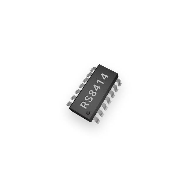
RS8414
TSSOP-14
5.00mm x 4.40mm
(1) For all available packages, see the orderable addendum
at the end of the data sheet.
1 / 14
www.run-ic.com
�RS841X
Revision History
Note: Page numbers for previous revisions may different from page numbers in the current version.
Version
A.1
Change Date
2020/12/5
A.2
2021/6/24
Change Item
Initial version completed
1、Added the value of Input Voltage Noise Density
2、Added the information of package size
3、Updated IQ values in Page 8 @A.1 Version
2 / 16
www.run-ic.com
�RS841X
Pin Configuration and Functions (Top View)
RS8411
1
V-
2
+IN
3
5
V+
+IN
1
V-
2
-IN
3
5
V+
4
OUT
+
OUT
RS8411B
+
-
4
-IN
SOT23-5
-
SOT23-5
Pin Description
NAME
PIN
RS8411B
1
I/O
+IN
RS8411
3
V-
2
2
-
-IN
OUT
V+
4
1
5
3
4
5
I
O
-
I
DESCRIPTION
Positive (noninverting) input
Negative (lowest) power supply or ground (for single supply
operation)
Negative (inverting) input
Output
Positive (highest) power supply
3 / 16
www.run-ic.com
�RS841X
Pin Configuration and Functions (Top View)
RS8412
OUT A
1
-IN A
2
+IN A
3
V-
4
+
A
B+
8
V+
7
OUTB
6
-IN B
5
+IN B
SOIC-8(SOP8)/MSOP8
Pin Description
-INA
+INA
-INB
+INB
OUTA
OUTB
PIN
SOIC-8(SOP8)/MSOP-8
2
3
6
5
1
7
V-
4
-
V+
8
-
NAME
I/O
DESCRIPTION
I
I
I
I
O
O
Inverting input, channel A
Noninverting input, channel A
Inverting input, channel B
Noninverting input, channel B
Output, channel A
Output, channel B
Negative (lowest) power supply or ground (for single supply
operation)
Positive (highest) power supply
4 / 16
www.run-ic.com
�RS841X
Pin Configuration and Functions (Top View)
RS8414
OUT A
1
-IN A
2
+IN A
14
OUT D
13
-IN D
3
12
+IN D
V+
4
11
V-
+IN B
5
10
+IN C
-IN B
6
9
-IN C
OUT B
7
8
OUT C
A
- +
D
+ -
- +
B
+ C
SOIC-14(SOP14),TSSOP-14
Pin Description
-INA
+INA
-INB
+INB
-INC
+INC
-IND
+IND
OUTA
OUTB
OUTC
OUTD
PIN
SOIC-14(SOP14)/TSSOP-14
2
3
6
5
9
10
13
12
1
7
8
14
V-
11
-
V+
4
-
NAME
I/O
DESCRIPTION
I
I
I
I
I
I
I
I
O
O
O
O
Inverting input, channel A
Noninverting input, channel A
Inverting input, channel B
Noninverting input, channel B
Inverting input, channel C
Noninverting input, channel C
Inverting input, channel D
Noninverting input, channel D
Output, channel A
Output, channel B
Output, channel C
Output, channel D
Negative (lowest) power supply or ground (for
single supply operation)
Positive (highest) power supply
5 / 16
www.run-ic.com
�RS841X
SPECIFICATIONS
Absolute Maximum Ratings
Over operating free-air temperature range (unless otherwise noted) (1)
MIN
MAX
-0.7
36
(V-)-0.2
(V+) +0.2
(V-)-0.2
(V+) +0.2
-10
10
-100
100
Continuous
-40
125
150
-55
150
Supply, Vs=(V+) - (V-)
Signal input pin (2)
Signal output pin (3)
Signal input pin (2)
Signal output pin (3)
Output short-circuits (4)
Operating range, TA
Junction, TJ
Storage, Tstg
Voltage
Current
Temperature
UNIT
V
mA
mA
°C
(1) Stresses above these ratings may cause permanent damage. Exposure to absolute maximum conditions for extended periods may degrade device
reliability. These are stress ratings only, and functional operation of the device at these or any other conditions beyond those specified is not implied.
(2) Input terminals are diode-clamped to the power-supply rails. Input signals that can swing more than 0.5V beyond the supply rails should be currentlimited to 10mA or less.
(3) Output terminals are diode-clamped to the power-supply rails. Output signals that can swing more than 0.5V beyond the supply rails should be currentlimited to ±100mA or less.
(4) Short-circuit to ground, one amplifier per package.
ESD Ratings
VALUE
V(ESD)
(1)
Electrostatic discharge
Human-body model (HBM)
±5000
Machine Model (MM)
±200
UNIT
V
JEDEC document JEP155 states that 500-V HBM allows safe manufacturing with a standard ESD control process.
Recommended Operating Conditions
Over operating free-air temperature range (unless otherwise noted)
MIN
Supply voltage,Vs= (V+) - (V-)
Single-supply
Dual-supply
NOM
MAX
3
36
±1.5
±18
UNIT
V
Thermal Information
THERMAL METRIC (1)
RS8411
5PINS
RS8412
8PINS
SOT23-5
SOIC-8
MSOP-8
RS8414
14PINS
TSSOPSOIC-14
14
UNIT
RϴJA
Junction-to-ambient thermal resistance
273.8
124.7
165
83.8
120.8
°C/W
RϴJC(top)
Junction-to-case(top) thermal resistance
126.8
66.9
53
70.7
34.3
°C/W
RϴJB
ѰJT
ѰJB
Junction-to-board thermal resistance
85.9
67.9
87
59.5
62.8
°C/W
Junction-to-top characterization parameter
Junction-to-board characterization parameter
10.9
84.9
19.2
67.2
4.9
85
11.6
37.7
10.5
56.5
°C/W
°C/W
RϴJC(bot)
Junction-to-case(bottom) thermal resistance
N/A
N/A
N/A
N/A
N/A
°C/W
6 / 16
www.run-ic.com
�RS841X
PACKAGE/ORDERING INFORMATION
Orderable
Device
Package Type
Pin
Channel
Op Temp(°C)
Device
Marking (1)
Package Qty
RS8411XF
SOT23-5
5
1
-40℃~125℃
8411
Tape and Reel,3000
RS8411BXF
SOT23-5
5
1
-40℃~125℃
8411B
Tape and Reel,3000
RS8412XK
SOIC-8(SOP8)
8
2
-40℃~125℃
RS8412
Tape and Reel,4000
RS8412XM
MSOP-8
8
2
-40℃~125℃
RS8412
Tape and Reel,4000
RS8414XP
SOIC-14(SOP14)
14
4
-40℃~125℃
RS8414
Tape and Reel,4000
RS8414XQ
TSSOP-14
14
4
-40℃~125℃
RS8414
Tape and Reel,4000
NOTE:
(1) There may be additional marking, which relates to the lot trace code information(data code and vendor code),the logo
or the environmental category on the device.
7 / 16
www.run-ic.com
�RS841X
ELECTRICAL CHARACTERISTICS
(At TA = +25C, Vs=3V to 36V, RL = 10kΩ connected to VS/2, and VOUT = VS/2, unless otherwise noted.)
PARAMETER
CONDITIONS
TJ
RS841X
MIN
TYP
MAX
150
200
36
250
350
UNITS
POWER SUPPLY
Vs
Operating Voltage Range
25C
3
Quiescent Current/Amplifier
Vs=±2.5V, Io=0mA
Vs=±18V, Io=0mA
25C
Power-Supply Rejection
Ratio
Vs=5V to 36V
25C
98
120
Vos
Input Offset Voltage
VCM= VS/2
25C
-40C to 125C
-4
±0.8
±1.1
Vos Tc
Input Offset Voltage
Average Drift
IQ
PSRR
V
uA
dB
INPUT
IB
Input Bias Current
VCM=0V
IOS
Input Offset Current
VCM=0V
VCM
Common-Mode Voltage
Range
Vs= ±18V
Common-Mode Rejection
Ratio
Vs= ±2.5V, VCM=(V-)-0.1V
to (V+)-2V
Vs= ±18V, VCM=(V-)-0.1V
to (V+)-2V
CMRR
-40C to 125C
3
25C
-40C to 125C
25C
-40C to 125C
10
600
10
600
25C
(V-)-0.1
25C
70
25C
70
93
4
mV
uV/C
60
60
(V+)-2
pA
pA
V
110
dB
OUTPUT
AOL
VOH
VOL
ISC
CLOAD
Open-Loop Voltage Gain
RL=10KΩ, Vo=(V-)-0.6V to
(V+)-0.6V
25C
Output Swing
Vs=±18V, RL=10KΩ
25C
Short-circuit current
Capacitive load drive
VS=36V, Vo=0V
25C
25C
70
100
V
V
mA
pF
G=+1, CL=100pF
25C
25C
0.67
1.2
V/us
MHz
25C
5
us
25C
25C
5
10
us
us
25C
16
uVpp
25C
45
nV/√Hz
115
dB
17.85
-17.85
FREQUENCY RESPONSE
SR
GBW
Slew Rate
Gain-Bandwidth Product
ts
Setting Time,0.01%
tOR
tON
Overload Recovery Time
Turn On Time
VS=±2.5V, G=+1,
CL=100pF, Step=2V
VIN·Gain≥VS,G=11
NOISE
En
Input Voltage Noise
en
Input Voltage Noise Density
f = 0.1Hz to 10Hz,
Vs=±2.5V
f = 1KHz
8 / 16
www.run-ic.com
�RS841X
TYPICAL CHARACTERISTICS
At TA = +25C, Vs=±18V, RL = 10kΩ connected to VS/2, VOUT = VS/2, unless otherwise noted.
OPEN-LOOP GAIN AND PHASE vs
FREQUENCY
Gain
Phase
90
Phase Margin (°)
100
Open-Loop Gain(dB)
SUPPLY VOLTAGE vs QUIESCENT CURRENT
500
110
80
70
60
50
40
30
20
10
0
-20
10
100
1K
10K
100K
1M
Quiescent Current(uA)
120
RS8412
450
400
350
300
250
200
150
100
-10
10M
0
2V/div
2V/div
Input
Output
12 16 20 24 28 32 36
Input
Output
VS=±18V
G=+1
CL=0PF
VS=±18V
G=+1
CL=100PF
100us/div
100us/div
SMALL SIGNAL STEP RESPONSE
SMALL SIGNAL STEP RESPONSE
Input
Output
Input
Output
50mV/div
50mV/div
8
LARGE SIGNAL STEP RESPONSE
LARGE SIGNAL STEP RESPONSE
VS=±18V
G=+1
CL=0PF
VS=±18V
G=+1
CL=100PF
100us/div
100us/div
|
4
Supply Voltage(V)
Frequency(Hz)
9 / 16
www.run-ic.com
�RS841X
TYPICAL CHARACTERISTICS
At TA = +25C, Vs=±18V, RL = 10kΩ connected to VS/2, VOUT = VS/2, unless otherwise noted.
20
2V/div
VOUT
0V
5us/div
5us/div
Output Voltage Swing vs Output Current
0.1Hz TO 10Hz NOISE AT Vs=5V
15
VOH
VOL
10
5
2uV/div
Output Voltage(V)
VIN
10V/div
VOUT
Input
Output
VS=±18V
G=11
2V/div
0V
VIN
NEGATIVE OVERVOLTAGE RECOVERY
10V/div
POSITIVE OVERVOLTAGE RECOVERY
Input
VS=±18V
Output
G=11
0
-5
-10
-15
-20
0
10
20
30
40
50
60
1s/div
70
Output Current(mA)
10 / 16
www.run-ic.com
�RS841X
PACKAGE OUTLINE DIMENSIONS
SOT23-5
D
1.90
b
2.59
E1
E
0.99
0.95
0.69
e
e1
RECOMMENDED LAND PATTERN (Unit: mm)
0.2
A A2
L
A1
Symbol
c
θ
Dimensions In Millimeters
Dimensions In Inches
Min
Max
Min
Max
A
1.050
1.250
0.041
0.049
A1
0.000
0.100
0.000
0.004
A2
1.050
1.150
0.041
0.045
b
0.300
0.500
0.012
0.020
c
0.100
0.200
0.004
0.008
D
2.820
3.020
0.111
0.119
E
1.500
1.700
0.059
0.067
E1
2.650
2.950
0.104
0.116
e
0.950(BSC)
0.037(BSC)
e1
1.800
2.000
0.071
0.079
L
0.300
0.600
0.012
0.024
θ
0°
8°
0°
8°
11 / 16
www.run-ic.com
�RS841X
MSOP-8
b
e
E
E1
4.8
1.02
D
0.65
0.41
RECOMMENDED LAND PATTERN (Unit: mm)
A2
c
A
A1
L
Symbol
Dimensions In Millimeters
θ
Dimensions In Inches
Min
Max
Min
Max
A
0.820
1.100
0.032
0.043
A1
0.020
0.150
0.001
0.006
A2
0.750
0.950
0.030
0.037
b
0.250
0.380
0.010
0.015
c
0.090
0.230
0.004
0.009
D
2.900
3.100
0.114
0.122
e
0.650(BSC)
0.026(BSC)
E
2.900
3.100
0.114
0.122
E1
4.750
5.050
0.187
0.199
L
0.400
0.800
0.016
0.031
θ
0°
6°
0°
6°
12 / 16
www.run-ic.com
�RS841X
SOIC-8(SOP8)
b
e
5.2
E
E1
2.2
D
1.27
0.6
RECOMMENDED LAND PATTERN (Unit: mm)
A2
c
A
A1
L
Symbol
Dimensions In Millimeters
θ
Dimensions In Inches
Min
Max
Min
Max
A
1.350
1.750
0.053
0.069
A1
0.100
0.250
0.004
0.010
A2
1.350
1.550
0.053
0.061
b
0.330
0.510
0.013
0.020
c
0.170
0.250
0.007
0.010
D
4.800
5.000
0.189
0.197
e
1.270(BSC)
0.050(BSC)
E
5.800
6.200
0.228
0.244
E1
3.800
4.000
0.150
0.157
L
0.400
1.270
0.016
0.050
θ
0°
8°
0°
8°
13 / 16
www.run-ic.com
�RS841X
SOIC-14(SOP14)
e
b
5.2
1.27
E E1
0.6
D
1.27
RECOMMENDED LAND PATTERN (Unit: mm)
A2
A1
A
c
θ
L
Symbol
Dimensions In Millimeters
Dimensions In Inches
Min
Max
Min
Max
A
1.350
1.750
0.053
0.069
A1
0.100
0.250
0.004
0.010
A2
1.350
1.550
0.053
0.061
b
0.310
0.510
0.012
0.020
c
0.100
0.250
0.004
0.010
D
8.450
8.850
0.333
0.348
e
1.270(BSC)
0.050(BSC)
E
5.800
6.200
0.228
0.244
E1
3.800
4.000
0.150
0.157
L
0.400
1.270
0.016
0.050
θ
0°
8°
0°
8°
14 / 16
www.run-ic.com
�RS841X
TSSOP-14
e
b
5.6
E1 E
1.78
D
0.65
0.42
RECOMMENDED LAND PATTERN (Unit: mm)
A2
A
A1
Symbol
H
C
θ
L
Dimensions In Millimeters
Min
Max
A
Dimensions In Inches
Min
Max
1.200
0.047
A1
0.050
0.150
0.002
0.006
A2
0.800
1.050
0.031
0.041
b
0.190
0.300
0.007
0.012
c
0.090
0.200
0.004
0.008
D
4.860
5.100
0.191
0.201
E
4.300
4.500
0.169
0.177
E1
6.250
6.550
0.246
0.258
e
L
0.650(BSC)
0.500
H
θ
0.026(BSC)
0.700
0.020
0.25(TYP)
1°
0.028
0.01(TYP)
7°
15 / 16
1°
7°
www.run-ic.com
�RS841X
TAPE AND REEL INFORMATION
REEL DIMENSIONS
TAPE DIMENSION
Reel
Diameter
Reel Width(W1)
DIRECTION OF FEED
NOTE: The picture is only for reference. Please make the object as the standard.
KEY PARAMETER LIST OF TAPE AND REEL
Package
Type
SOT23-5
SOIC-8
(SOP8)
MSOP-8
SOIC-14
(SOP14)
TSSOP-14
Reel
Diameter
7’’
Reel Width
W1(mm)
9.5
A0
(mm)
3.20
B0
(mm)
3.20
K0
(mm)
1.40
P0
(mm)
4.0
P1
(mm)
4.0
P2
(mm)
2.0
W
(mm)
8.0
Pin1
Quadrant
Q3
13’’
12.4
6.40
5.40
2.10
4.0
8.0
2.0
12.0
Q1
13’’
12.4
5.20
3.30
1.50
4.0
8.0
2.0
12.0
Q1
13’’
16.4
6.60
9.30
2.10
4.0
8.0
2.0
16.0
Q1
13’’
12.4
6.95
5.60
1.20
4.0
8.0
2.0
14.0
Q1
16 / 16
www.run-ic.com
�