Advanced Science And Novel Technology Company, Inc.
2790 Skypark Dr., Ste #112, Torrance, CA 90505
Office: (310) 530-9400 Fax: (310) 530-9402
www.adsantec.com
ASNT6163-KHC
DC-32GHz Analog Signal Selector 1-of-2
1dB compression point of 0dBm
DC-to-1GHz broadband channel selector port
Optional two-channel mixer/adder setting available
Low jitter and limited temperature variation over industrial temperature range
Single +3.6V or -3.6V power supply
Power consumption: 700mW
Fabricated in SiGe for high performance, yield, and reliability
Custom CQFN 24-pin package
vee
Temperature-stabilized differential gain of approximately 0dB
vcc
d0p
Two differential CML-type input ports and one differential CML-type output port
vcc
d0n
DC to 32GHz broadband operation
vcc
on2
vcc
vcc
sel
qp
vcc
ASNT6163
ief1c
qn
1
vcc
d1n
vcc
d1p
vcc
vcc
vee
vcc
Rev. 0.0.2
vcc
ief3c
December 2019
�Advanced Science And Novel Technology Company, Inc.
2790 Skypark Dr., Ste #112, Torrance, CA 90505
Office: (310) 530-9400 Fax: (310) 530-9402
www.adsantec.com
DESCRIPTION
on2
50
d0p
d0n
50
50
ief1c/ief3c
50
d1p
d1n
qp
qn
50
50
sel
Fig. 1. Functional Block Diagram
The temperature stable ASNT6163-KHC analog signal selector 1-of-2 is intended for use in high-speed
systems. The IC shown in Fig. 1 can deliver one of two different broad-band analog differential signals
d0p/d0n and d1p/d1n to its differential output qp/qn with a nominal gain of 0dB. It can also be used as a
two-channel analog mixer/adder of signals d0p/d0n and d1p/d1n. Two low-speed analog current
controls Ief1c and Ief3c are available for bandwidth and peaking adjustments.
The active input selection is performed through the external high-speed single-ended port sel that can be
referenced to either vcc or vee. When the low-speed single-ended control port on2 is set to vcc, it
switches the circuit into mixer/adder mode with both inputs active at the same time.
The part’s I/O’s support the CML logic interface with on chip 50Ohm termination to vcc and may be used
differentially, AC/DC coupled, single-ended, or in any combination (also see Error! Not a valid
bookmark self-reference.). In the DC-coupling mode, the input signal’s common mode voltage should
comply with the specifications shown in ELECTRICAL CHARACTERISTICS. In the AC-coupling
mode, the input termination provides the required common mode voltage automatically.
POWER SUPPLY CONFIGURATION
The part can operate with either negative supply (vcc = 0.0V = ground and vee = −3.6V), or positive
supply (vcc = +3.6V and vee = 0.0V = ground). In case of the positive supply, all I/Os need AC
termination when connected to any devices with 50Ohm termination to ground.
Different PCB layouts will be needed for each different power supply combination.
All the characteristics detailed below assume vcc = 0.0V = ground.
Rev. 0.0.2
2
December 2019
�Advanced Science And Novel Technology Company, Inc.
2790 Skypark Dr., Ste #112, Torrance, CA 90505
Office: (310) 530-9400 Fax: (310) 530-9402
www.adsantec.com
ABSOLUTE MAXIMUM RATINGS
Caution: Exceeding the absolute maximum ratings shown in Table 1 may cause damage to this product
and/or lead to reduced reliability. Functional performance is specified over the recommended operating
conditions for power supply and temperature only. AC and DC device characteristics at or beyond the
absolute maximum ratings are not assumed or implied. All min and max voltage limits are referenced to
ground (assumed vcc).
Table 1. Absolute Maximum Ratings
Parameter
Supply Voltage (vee)
Power supply current
Input Voltage
RF Input Voltage Swing (SE)
Case Temperature
Storage Temperature
Operational Humidity
Storage Humidity
Min
vcc-1.2
-40
10
10
Max
-4.0
320
vcc-0.6
0.6
+90
+100
98
98
Units
V
mA
V
V
ºC
ºC
%
%
TERMINAL FUNCTION
TERMINAL
Name No.
Type
d0p
d0n
d1p
d1n
qp
qn
15
17
3
5
11
9
sel
21
ief1c
ief3c
23
7
on2
19
Name
vcc
vee
Rev. 0.0.2
CML type
CML type
CML type
DESCRIPTION
High-speed Signals
Differential high speed data inputs with internal SE 50Ohm
termination to vcc
Differential high speed data outputs with internal SE 50Ohm
termination to vcc. Require external SE 50Ohm termination to vcc
Control Signals
SE
High-speed high-impedance input (active: high, d1 is connected to
q default: low, d0 is connected to q;)
Analog Analog current control with internal 64KOhm termination to vcc
Control and 72KOhm termination to vee.
Low-speed high-impedance input (active: high, mixer/adder mode;
CMOS
default: low, 1-of-2 selector mode;)
Supply and Termination Voltages
Description
Pin Number
Positive power supply rail
2, 4, 6, 8, 10, 12, 14, 16, 18, 20, 22, 24
Negative power supply rail
1, 13
3
December 2019
�Advanced Science And Novel Technology Company, Inc.
2790 Skypark Dr., Ste #112, Torrance, CA 90505
Office: (310) 530-9400 Fax: (310) 530-9402
www.adsantec.com
ELECTRICAL CHARACTERISTICS
PARAMETER
MIN
vee
vcc
Ivee
Power consumption
Junction temperature
Bandwidth
Common mode level
Voltage swing, pk-pk
S11
Control range
Default voltage level
Bandwidth
Common mode level
Small Signal Differential Gain
Output referred 1dB
Compression Point
THD
High logic level
Low logic level
Bandwidth
High logic level
Low logic level
Input current
Rev. 0.0.2
TYP MAX
UNIT
COMMENTS
General Parameters
-3.4
-3.6
-3.8
V
±5.5%
0.0
V
External ground
200
mA
In Selector Mode
280
mA
In Mixer/Adder Mode
700
mW
In Selector Mode
1000
mW
In Mixer/Adder Mode
-25
50
125
°C
Input Analog (d0p/d0n, d1p/d1n)
DC
32
GHz
-3dB
mV
AC-coupled
vcc
Single-ended, with unused input not
0
400
mV
connected or AC terminated
0
800
mV
Differential
-35
dB
at 3GHz
-16
dB
at 10GHz
-11
dB
at 20GHz
-9
dB
at 25GHz
Current Control Signals (ief1c/ief3c)
V
vee
vcc
V
at ±3.6V supply
vee+1.9
Output Analog (qp/qn)
DC
32
GHz
-3dB
With external 50Ohm
vcc-0.55
V
DC termination
-1.5
0.0
+1.5
dB
up to 25GHz
1
dBm
0.5
%
0.6
%
1.9
%
2.5
%
Low-Speed Control (on2)
V
vcc
V
vee
High-Speed Control (sel)
1
GHz
V
vcc
V
vee
20 uA
4
Single-Ended, 20GHz
at 1GHz
at 10GHz
at 25GHz
at 35GHz
Mixer/Adder Mode
1-of-2 Selector Mode
Input d1p/d1n is active
Input d0p/d0n is active
sink or source
December 2019
�Advanced Science And Novel Technology Company, Inc.
2790 Skypark Dr., Ste #112, Torrance, CA 90505
Office: (310) 530-9400 Fax: (310) 530-9402
www.adsantec.com
PACKAGE INFORMATION
The chip die is housed in a custom 24-pin CQFN package shown in Fig. 2. The package provides a center
heat slug located on its back side to be used for heat dissipation. ADSANTEC recommends for this
section to be soldered to the vcc plain, which is ground for a negative supply, or power for a positive
supply.
Fig. 2. CQFN 24-Pin Package Drawing (All Dimensions in mm)
Rev. 0.0.2
5
December 2019
�Advanced Science And Novel Technology Company, Inc.
2790 Skypark Dr., Ste #112, Torrance, CA 90505
Office: (310) 530-9400 Fax: (310) 530-9402
www.adsantec.com
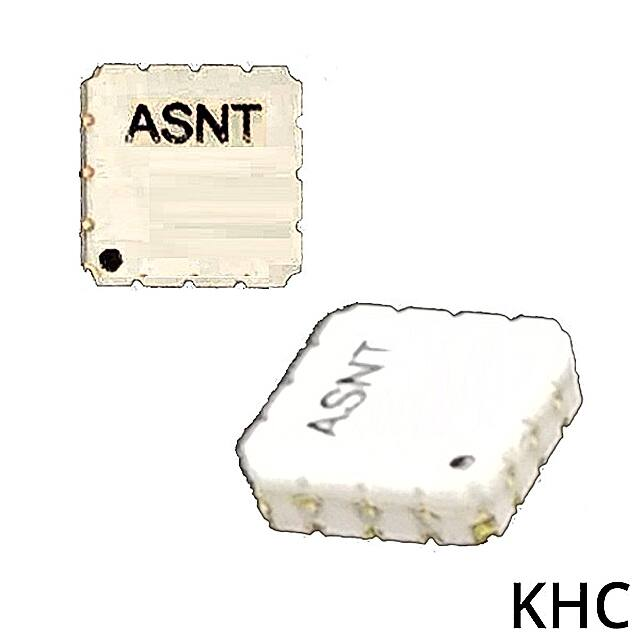
The part’s identification label is ASNT6163-KHC. The first 8 characters of the name before the dash
identify the bare die including general circuit family, fabrication technology, specific circuit type, and part
version while the 3 characters after the dash represent the package’s manufacturer, type, and pin out
count.
This device complies with the Restriction of Hazardous Substances (RoHS) per EU 2011/65/EU for all
ten substances.
REVISION HISTORY
Revision
0.0.2
Rev. 0.0.2
Date
12-2019
Changes
Preliminary release
6
December 2019
�