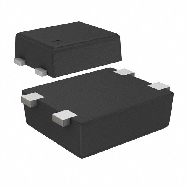
S-5813A/5814A Series
www.ablic.com
www.ablicinc.com
CMOS TEMPERATURE SENSOR IC
Rev.4.1_02
© ABLIC Inc., 2006-2015
The S-5813A/5814A Series is a family of high-precision temperature sensor ICs on a single chip with a linear output voltage for
temperature changes.
Each chip is composed of a temperature sensor, a constant current circuit, and an operational amplifier.
The operating ambient temperature is from –40C to 100C. These devices have much better linearity than other temperature
sensors such as thermistors, and can be used for a wide range of temperature control applications.
Features
Temperature accuracy
Linear output voltage
Nonlinearity
Wide power supply voltage operation
Low current consumption
Built-in operational amplifier
Output voltage referred to VSS
Lead-free (Sn 100%), halogen-free
S-5813A Series : 5.0C (–30C to 100C)
S-5814A Series : 2.5C (–30C to 100C)
–11.04 mV/C typ.
Ta = 30C :
2.582 V typ.
Ta = 30C :
1.940 V typ.
Ta = 100C : 1.145 V typ.
0.5% typ. (–20C to 80C)
VDD = 2.4 V to 10.0 V (25C)
4.0 A typ. (25C)
Applications
Compensation of high-frequency circuits such as cellular phones and radio equipment
Compensation of oscillation frequency in crystal oscillator
LCD contrast compensation
Compensation of amplifier gain
Compensation of auto focus circuits
Temperature detection in battery management
Overheating prevention for charged batteries or halogen lights
Package
SNT-4A
1
�CMOS TEMPERATURE SENSOR IC
S-5813A/5814A Series
Rev.4.1_02
Block Diagram
VDD
VOUT
Temperature sensor
VSS
Figure 1
2
�CMOS TEMPERATURE SENSOR IC
S-5813A/5814A Series
Rev.4.1_02
Product Name Structure
Users can select the product type for the S-5813A/5814A Series. Refer to “1. Product name” regarding the contents of
product name, “2. Package” regarding the package drawings, “3. Product name list” regarding details of the product
name.
1. Product name
S-581
x
A -
I4T1
U
Environmental code
U : Lead-free (Sn 100%), halogen-free
Package name (abbreviation) and packing specifications
I4T1 : SNT-4A, Tape
*1
Product type
3 : Temperature accuracy 5.0°C
4 : Temperature accuracy 2.5°C
*1. Refer to the tape drawing.
2. Package
Package Name
Package
PF004-A-P-SD
SNT-4A
Drawing Code
Tape
Reel
PF004-A-C-SD
PF004-A-R-SD
Land
PF004-A-L-SD
3. Product name list
Table 1
Product Name
S-5813A-I4T1U
S-5814A-I4T1U
Temperature Accuracy
5.0C
2.5C
3
�CMOS TEMPERATURE SENSOR IC
S-5813A/5814A Series
Rev.4.1_02
Pin Configuration
SNT-4A
Table 2
Top view
Pin No.
1
4
2
3
Figure 2
4
Pin Name
Pin Description
1
VSS
GND pin
2
VDD
Power supply pin
3
VOUT
Output voltage pin
NC*1
4
No connection
*1. The NC pin is electrically open.
The NC pin can be connected to the VDD pin or the VSS pin.
�CMOS TEMPERATURE SENSOR IC
S-5813A/5814A Series
Rev.4.1_02
Absolute Maximum Ratings
Table 3
Item
Symbol
Power supply voltage
VDD
Output voltage
VOUT
(Ta = 25C unless otherwise specified)
Absolute Maximum Rating
Unit
VSS – 0.3 to VSS 12.0
V
VSS – 0.3 to VDD 0.3
V
140 (When not mounted on board)
mW
300*1
mW
Power dissipation
PD
Operating ambient temperature
Topr
–40 to 100
C
Storage temperature
Tstg
–40 to 125
C
*1. When mounted on board
[Mounted board]
(1) Board size :
114.3 mm 76.2 mm t1.6 mm
(2) Board name : JEDEC STANDARD51-7
Caution The absolute maximum ratings are rated values exceeding which the product could suffer physical
damage. These values must therefore not be exceeded under any conditions.
5
�CMOS TEMPERATURE SENSOR IC
S-5813A/5814A Series
Rev.4.1_02
Electrical Characteristics
1. S-5813A Series
Item
Power supply voltage
Output voltage
Table 4
(Ta = 25C, VDD = 5.0 V, IOUT = 0 A unless otherwise specified)
Test
Conditions
Min.
Typ.
Max.
Unit
Circuit
Symbol
2.40
10.00
V
1
Ta = 20C to 100C
2.65
10.00
V
1
Ta = 30C to 100C
2.90
10.00
V
1
VDD
VOUT
Ta = 30C
2.528
2.582
2.636
V
1
Ta = 30C
1.886
1.940
1.994
V
1
1.145
1.199
V
1
mV/C
Ta = 100C
1.091
VSE
Ta = 30C to 100C
11.31 11.04 10.77
Nonlinearity
NL
Ta = 20C to 80C
Operating temperature range
Topr
Temperature sensitivity
0.5
%
40
100
C
Current consumption
IDD
4.0
8.0
A
1
Line regulation
VOUT1
VDD = 2.4 V to 10.0 V
0.05
%/V
2
Load regulation*1
VOUT2
IOUT = 0 A to 200 A
1.0
mV
2
*1. Do not flow current into the output voltage pin.
2. S-5814A Series
Item
Power supply voltage
Output voltage
Table 5
(Ta = 25C, VDD = 5.0 V, IOUT = 0 A unless otherwise specified)
Test
Conditions
Min.
Typ.
Max.
Unit
Circuit
Symbol
2.40
10.00
V
1
Ta = 20C to 100C
2.65
10.00
V
1
Ta = 30C to 100C
2.90
10.00
V
1
VDD
VOUT
Ta = 30C
2.555
2.582
2.609
V
1
Ta = 30C
1.913
1.940
1.967
V
1
1.145
1.172
V
1
mV/C
Ta = 100C
1.118
VSE
Ta = 30C to 100C
11.31 11.04 10.77
Nonlinearity
NL
Ta = 20C to 80C
Operating temperature range
Topr
Temperature sensitivity
0.5
%
100
C
Current consumption
IDD
4.0
8.0
A
1
Line regulation
VOUT1
VDD = 2.4 V to 10.0 V
0.05
%/V
2
Load regulation*1
VOUT2
IOUT = 0 A to 200 A
1.0
mV
2
*1. Do not flow current into the output voltage pin.
6
40
�CMOS TEMPERATURE SENSOR IC
S-5813A/5814A Series
Rev.4.1_02
Test Circuits
1.
A
VDD
S-5813A/5814A
Series
VOUT
VSS
V
V
CIN
Figure 3
2.
VDD
S-5813A/5814A
Series
VOUT
A
VSS
V
V
CIN
IOUT
Figure 4
7
�CMOS TEMPERATURE SENSOR IC
S-5813A/5814A Series
Rev.4.1_02
Explanation of Terms
1. Output voltage (VOUT)
VOUT indicates the output voltage at Ta = –30C, Ta = 30C, and Ta = 100C.
Output voltage (VOUT)
Max.
Min.
30C
0C
30C
Temperature (Ta)
Figure 5
8
100C
�CMOS TEMPERATURE SENSOR IC
S-5813A/5814A Series
Rev.4.1_02
2. Temperature sensitivity (VSE)
VSE indicates the temperature coefficient of the output voltage calculated using the output voltage at Ta = 30C and
Ta = 100C.
VSE is calculated using the following formula.
VSE
V
OUT
*1
VOUT *2
130 *3
Output voltage (VOUT)
VOUT (at Ta = 30C)
VSE
VOUT (at Ta = 100C)
30C
0C
30C
100C
Temperature (Ta)
Figure 6
*1. VOUT value [V] at Ta = 100C.
*2. VOUT value [V] at Ta = 30C.
*3. The difference of the temperature [C] from Ta = 100C to Ta = 30C.
9
�CMOS TEMPERATURE SENSOR IC
S-5813A/5814A Series
Rev.4.1_02
3. Nonlinearity (NL)
NL indicates the nonlinearity of the output voltage and is defined as the difference of the characteristic curve of the output
voltage and the approximated straight line shown below.
NL is calculated using the following formula.
∆NL
a *1
100
b*2
Output voltage (VOUT)
a
VOUT (at Ta = 20C)
a
(B) Actual measurement
of output voltage
b
a
(A) Approximated straight line
VOUT (at Ta = 80C)
80C
20C 0C
Temperature (Ta)
*1. The maximum deviation of the actual measurement of output voltage (B) and an approximated straight line (A)
in temperature within 20C to 80C. (An approximated straight line is taken as the straight line when the “a”
becomes the minimum.)
*2. The difference of the output voltage within 20C to 80C.
Figure 7
4. Line regulation (VOUT1)
VOUT1 indicates the output voltage dependency of the input voltage. That is, the values express how the output voltage
changes, when input voltage is changed under the condition that output current is fixed.
5. Load regulation (VOUT2)
VOUT2 indicates the output voltage dependency of the output current. That is, the values express how the output
voltage changes, when output current is changed under the condition that input voltage is fixed.
10
�CMOS TEMPERATURE SENSOR IC
S-5813A/5814A Series
Rev.4.1_02
Precautions
Wiring patterns for the VDD pin, VSS pin, and VOUT pin should be designed to hold low impedance.
In this IC, if load capacitance of the VOUT pin is large, VOUT pin voltage may oscillate. It is recommended not to use the
external capacitor between the VOUT and VSS pin. When using an external capacitor, mount it near the VOUT pin.
When connecting an A/D converter etc. to the VOUT pin, the input pin capacitance of the A/D converter and the parasitic
capacitance component between wires are included as load capacitance.
To prevent oscillation, it is recommended to use the following output load condition.
Load capacitance of VOUT pin (CL) : 2.2 F or less
VDD
S-5813A/5814A
Series
VOUT
VSS
CL
CIN
VOUT
Figure 8
Caution The above connection diagram and constant will not guarantee successful operation. Perform
through evaluation using the actual application to set the constant.
Please do not connect a pull-up resistor to the output voltage pin.
The application condition for input voltage, output voltage and load voltage must not exceed the package power
dissipation.
Do not apply an electrostatic discharge to this IC that exceeds the performance ratings of the built-in electrostatic
protection circuit.
ABLIC Inc. claims no responsibility for any disputes arising out of or in connection with any infringement by products
including this IC of patents owned by a third party.
11
�CMOS TEMPERATURE SENSOR IC
S-5813A/5814A Series
Rev.4.1_02
Characteristics (Typical Data)
3.0
2.8
2.6
2.4
2.2
2.0
1.8
1.6
1.4
1.2
1.0
−40 −20
0
+20 +40 +60 +80 +100
Ta [°C]
+4
Approximated straight line:
VOUT [mV] = −11.02 [mV/°C] × Ta [°C] + 2245 [mV]
0
−2
−4
−40 −20
0
VDD = 10.0 V
VDD = 5.0 V
VDD = 2.4 V
−40 −20
0
+20 +40 +60 +80 +100
Ta [°C]
4. Current consumption (IDD) vs. Power supply voltage (VDD)
+2
−6
10.0
9.0
8.0
7.0
6.0
5.0
4.0
3.0
2.0
1.0
0
IDD [μA]
Difference between the temperature
converted into approximated straight
line and actual temperature [C]
3. Error range of each temperature
+6
2. Current consumption (IDD) vs. Temperature (Ta)
IDD [μA]
VOUT [V]
1. Output voltage (VOUT) vs. Temperature (Ta)
10
9
8
7
6
5
4
3
2
1
0
Ta = −40°C
Ta = +30°C
Ta = +100°C
2.0 3.0 4.0 5.0 6.0 7.0 8.0 9.0 10.0
VDD [V]
+20 +40 +60 +80 +100
Ta [°C]
2.684
2.683
2.682
2.681
2.680
2.679
2.678
2.677
2.676
2.675
2.674
Ta = −40°C
VOUT [V]
VOUT [V]
5. Output voltage (VOUT) vs. Power supply voltage (VDD)
VOUT [V]
2.0 3.0 4.0 5.0 6.0 7.0 8.0 9.0 10.0
VDD [V]
1.150
1.149
1.148
1.147
1.146
1.145
1.144
1.143
1.142
1.141
1.140
Ta = +100°C
2.0 3.0 4.0 5.0 6.0 7.0 8.0 9.0 10.0
VDD [V]
12
1.941
1.940
1.939
1.938
1.937
1.936
1.935
1.934
1.933
1.932
1.931
Ta = +30°C
2.0 3.0 4.0 5.0 6.0 7.0 8.0 9.0 10.0
VDD [V]
�CMOS TEMPERATURE SENSOR IC
S-5813A/5814A Series
Rev.4.1_02
6. Output voltage (VOUT) vs. Load current (IOUT)
VDD = 2.4 V
3.0
Ta = −40°C
2.5
2.0
VOUT [V]
VOUT [V]
2.5
Ta = +30°C
1.5
1.0
Ta = +100°C
0.5
Ta = −40°C
2.0
Ta = +30°C
1.5
1.0
Ta = +100°C
0.5
0
0
0 0.1 0.2 0.3 0.4 0.5 0.6 0.7 0.8 0.9 1.0
IOUT [mA]
0
0.5 1.0 1.5 2.0 2.5 3.0 3.5 4.0
IOUT [mA]
VDD = 10.0 V
3.0
2.5
VOUT [V]
VDD = 5.0 V
3.0
Ta = −40°C
2.0
Ta = +30°C
1.5
1.0
Ta = +100°C
0.5
0
0
4.0
2.0
8.0
6.0
IOUT [mA]
10.0
12.0
7. Heat response Output voltage (VOUT) vs. Time (t)
When package is put into the liquid of 100C from the
air of 25C
2.1
2.0
1.9
1.8
1.7
1.6
1.5
1.4
1.3
1.2
1.1
0
20
40
60
10
30
50
t [s]
VOUT [V]
VOUT [V]
When package is put into the air of 100C from the air
of 25C
2.1
2.0
1.9
1.8
1.7
1.6
1.5
1.4
1.3
1.2
1.1
0 30 60 90 120 150 180 210 240
t [s]
8. Start up response
Ta = +25°C, CL = 100 pF, RL = 10 MΩ
VDD
(= 5.0 V)
1 V / div.
VOUT
1 V / div.
GND
GND
t (50 μs / div.)
Ta = +25°C, CL = 100 pF, RL = 10 MΩ
1 V / div.
VDD
(= 2.4 V)
GND
1 V / div.
VOUT
GND
t (50 μs / div.)
13
�CMOS TEMPERATURE SENSOR IC
S-5813A/5814A Series
Rev.4.1_02
Marking Specification
1. SNT-4A
Top view
(1) to (3) :
1
4
(1) (2) (3)
2
3
Product name vs. Product code
Product Name
S-5813A-I4T1U
S-5814A-I4T1U
14
Product Code
(1)
(2)
(3)
D
R
C
D
R
D
Product code (refer to Product name vs. Product code)
�1.2±0.04
3
4
+0.05
0.08 -0.02
2
1
0.65
0.48±0.02
0.2±0.05
No. PF004-A-P-SD-6.0
TITLE
SNT-4A-A-PKG Dimensions
No.
PF004-A-P-SD-6.0
ANGLE
UNIT
mm
ABLIC Inc.
�+0.1
ø1.5 -0
4.0±0.1
2.0±0.05
0.25±0.05
+0.1
1.45±0.1
2
1
3
4
ø0.5 -0
4.0±0.1
0.65±0.05
Feed direction
No. PF004-A-C-SD-2.0
TITLE
SNT-4A-A-Carrier Tape
No.
PF004-A-C-SD-2.0
ANGLE
UNIT
mm
ABLIC Inc.
�12.5max.
9.0±0.3
Enlarged drawing in the central part
ø13±0.2
(60°)
(60°)
No. PF004-A-R-SD-1.0
TITLE
SNT-4A-A-Reel
No.
PF004-A-R-SD-1.0
QTY.
ANGLE
UNIT
mm
ABLIC Inc.
5,000
�0.52
1.16
2
0.52
0.35
1.
2.
0.3
1
(0.25 mm min. / 0.30 mm typ.)
(1.10 mm ~ 1.20 mm)
0.03 mm
1. Pay attention to the land pattern width (0.25 mm min. / 0.30 mm typ.).
2. Do not widen the land pattern to the center of the package (1.10 mm to 1.20 mm).
Caution 1. Do not do silkscreen printing and solder printing under the mold resin of the package.
2. The thickness of the solder resist on the wire pattern under the package should be 0.03 mm
or less from the land pattern surface.
3. Match the mask aperture size and aperture position with the land pattern.
4. Refer to "SNT Package User's Guide" for details.
1.
2.
(0.25 mm min. / 0.30 mm typ.)
(1.10 mm ~ 1.20 mm)
TITLE
SNT-4A-A
-Land Recommendation
PF004-A-L-SD-4.1
No.
No. PF004-A-L-SD-4.1
ANGLE
UNIT
mm
ABLIC Inc.
�Disclaimers (Handling Precautions)
1.
All the information described herein (product data, specifications, figures, tables, programs, algorithms and
application circuit examples, etc.) is current as of publishing date of this document and is subject to change without
notice.
2.
The circuit examples and the usages described herein are for reference only, and do not guarantee the success of
any specific mass-production design.
ABLIC Inc. is not liable for any losses, damages, claims or demands caused by the reasons other than the products
described herein (hereinafter "the products") or infringement of third-party intellectual property right and any other
right due to the use of the information described herein.
3.
ABLIC Inc. is not liable for any losses, damages, claims or demands caused by the incorrect information described
herein.
4.
Be careful to use the products within their ranges described herein. Pay special attention for use to the absolute
maximum ratings, operation voltage range and electrical characteristics, etc.
ABLIC Inc. is not liable for any losses, damages, claims or demands caused by failures and / or accidents, etc. due to
the use of the products outside their specified ranges.
5.
Before using the products, confirm their applications, and the laws and regulations of the region or country where they
are used and verify suitability, safety and other factors for the intended use.
6.
When exporting the products, comply with the Foreign Exchange and Foreign Trade Act and all other export-related
laws, and follow the required procedures.
7.
The products are strictly prohibited from using, providing or exporting for the purposes of the development of
weapons of mass destruction or military use. ABLIC Inc. is not liable for any losses, damages, claims or demands
caused by any provision or export to the person or entity who intends to develop, manufacture, use or store nuclear,
biological or chemical weapons or missiles, or use any other military purposes.
8.
The products are not designed to be used as part of any device or equipment that may affect the human body, human
life, or assets (such as medical equipment, disaster prevention systems, security systems, combustion control
systems, infrastructure control systems, vehicle equipment, traffic systems, in-vehicle equipment, aviation equipment,
aerospace equipment, and nuclear-related equipment), excluding when specified for in-vehicle use or other uses by
ABLIC, Inc. Do not apply the products to the above listed devices and equipments.
ABLIC Inc. is not liable for any losses, damages, claims or demands caused by unauthorized or unspecified use of
the products.
9.
In general, semiconductor products may fail or malfunction with some probability. The user of the products should
therefore take responsibility to give thorough consideration to safety design including redundancy, fire spread
prevention measures, and malfunction prevention to prevent accidents causing injury or death, fires and social
damage, etc. that may ensue from the products' failure or malfunction.
The entire system in which the products are used must be sufficiently evaluated and judged whether the products are
allowed to apply for the system on customer's own responsibility.
10. The products are not designed to be radiation-proof. The necessary radiation measures should be taken in the
product design by the customer depending on the intended use.
11. The products do not affect human health under normal use. However, they contain chemical substances and heavy
metals and should therefore not be put in the mouth. The fracture surfaces of wafers and chips may be sharp. Be
careful when handling these with the bare hands to prevent injuries, etc.
12. When disposing of the products, comply with the laws and ordinances of the country or region where they are used.
13. The information described herein contains copyright information and know-how of ABLIC Inc. The information
described herein does not convey any license under any intellectual property rights or any other rights belonging to
ABLIC Inc. or a third party. Reproduction or copying of the information from this document or any part of this
document described herein for the purpose of disclosing it to a third-party is strictly prohibited without the express
permission of ABLIC Inc.
14. For more details on the information described herein or any other questions, please contact ABLIC Inc.'s sales
representative.
15. This Disclaimers have been delivered in a text using the Japanese language, which text, despite any translations into
the English language and the Chinese language, shall be controlling.
2.4-2019.07
www.ablic.com
�