IS32LT3177/78
10-TO-200MA CONSTANT-CURRENT LED DRIVER FOR AUTOMOTIVE
September 2020
GENERAL DESCRIPTION
FEATURES
The IS32LT3177 and IS32LT3178 are adjustable
linear current devices with excellent temperature
stability. A single resistor is all that is required to set
the operating current from 10mA to 200mA. The
devices can operate from an input voltage from 2.9V
to 40V with a minimal voltage headroom of 1.0V
(Typ.) at 150mA. Designed with a low dropout
voltage; the device can drive LED strings close to
the supply voltage without switch capacitors or
inductors.
The IS32LT3177/78 simplifies designs by
providing a stable current without the additional
requirement of inductors, FETs or diodes. The
complete constant current driver requires only a
current set resistor and a small PCB area making
designs both efficient and cost effective.
The EN Pin of the IS32LT3177 can be tied to VBAT
or PSM (Power Supply Modulation) signal for high
side dimming. The EN Pin of the IS32LT3178 can
function as the PWM signal input used for MCU
PWM dimming.
As a current sink it is ideal for LED lighting
applications or current limiter for power supplies.
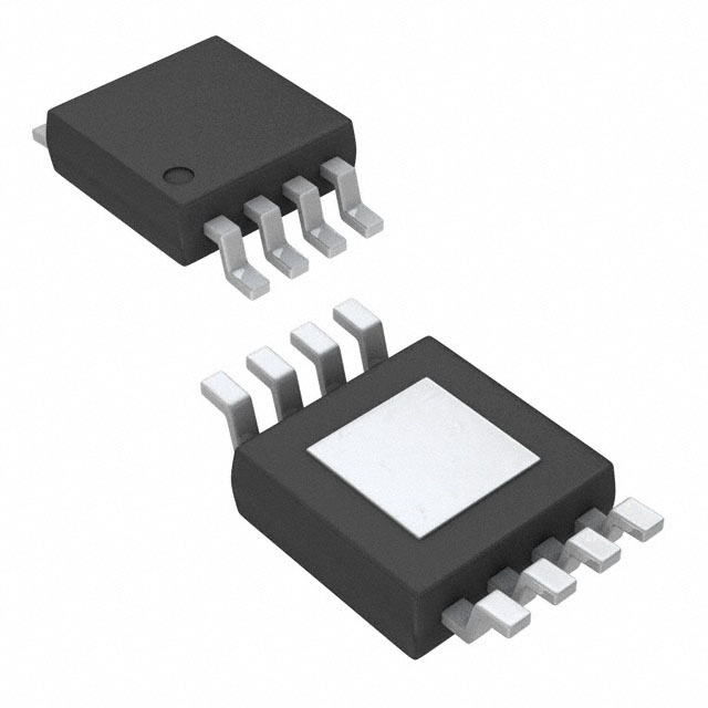
The device is provided in a lead (Pb) free, SOT23-6
and SOP-8-EP packages.
Lumissil Microsystems – www.lumissil.com
Rev. B, 09/25/2020
Low-side current sink
- Adjustable from 10mA to 150mA (SOT236)/200mA (SOP-8-EP) with external resistor
selection
Wide input voltage range from
- 2.9V to 40V (IS32LT3178)
- 5V to 40V (IS32LT3177)
with a low dropout of typical 1.0V at 150mA
Up to 1kHz PWM input (IS32LT3178 only)
Protection features:
- 0.6%/K current roll off at high temp over 145°C
for thermal protection
- Output current limit
- Thermal shutdown
Up to 0.77W (SOT23-6)/2.32W (SOP-8-EP)
power dissipation in a small package
RoHS compliant (Pb-free) package
AEC-Q100 Qualified
APPLICATIONS
Automotive and avionic lighting
Stop/tail light
Turn light
Retail lighting in fridge, freezer case and
vending machines
1
�IS32LT3177/78
TYPICAL APPLICATION CIRCUIT
VBAT
or
PSM
VBAT
CIN
0.1µF
1
6
EN
GND
2.9V~5.5V
or
2, 4, 5
IS32LT3177
(SOT23-6)
PWM
6
ISET
OUT
RISET
1
3
Optional
COUT
1nF
EN
GND
2, 4, 5
IS32LT3178
(SOT23-6)
ISET
OUT
RISET
VBAT
or
PSM
CIN
0.1µF
3
Optional
COUT
1nF
VBAT
CIN
0.1µF
3
4
RISET
EN
GND
2.9V~5.5V
or
5~8
IS32LT3177
(SOP-8-EP)
3
PWM
4
ISET
OUT
1,2
RISET
EN
GND
CIN
0.1µF
5~8
IS32LT3178
(SOP-8-EP)
ISET
OUT
1,2
Optional
COUT
1nF
Optional
COUT
1nF
Figure 1 Typical Application Circuit
Note 1: All GND pins must be connected to ground.
Note 2: CIN must be placed close to IC. If no PSM dimming requirement, please use larger value for CIN.
Note 3: COUT is optional. When the LED connection wire is long, the COUT should be placed close to OUT pin to avoid EMI interference.
Note 4: RISET MUST be placed close to ISET and GND pins to improve the Electro-Magnetic Susceptibility (EMS) performance.
Lumissil Microsystems – www.lumissil.com
Rev. B, 09/25/2020
2
�IS32LT3177/78
PIN CONFIGURATION
Package
Pin Configuration (Top View)
SOT23-6
SOP-8-EP
PIN DESCRIPTION
No.
SOT23-6 SOP-8-EP
Pin
Description
3
1, 2
OUT
Current sink.
1
3
EN
Enable pin (PWM input IS32LT3178 only).
6
4
ISET
Output current setting pin. Connect a resistor
between this pin and GND to set the maximum
output current.
2, 4, 5
5~8
GND
Ground pin. All GND pins must be connected to
supply ground.
-
Thermal Pad Connect to GND.
Lumissil Microsystems – www.lumissil.com
Rev. B, 09/25/2020
3
�IS32LT3177/78
ORDERING INFORMATION
Automotive Range: -40°C to +125°C
Order Part No.
Package
QTY/Reel
IS32LT3177-STLA3-TR
IS32LT3178-STLA3-TR
SOT23-6, Lead-free
3000
IS32LT3177-GRLA3-TR
IS32LT3178-GRLA3-TR
SOP-8-EP, Lead-free
2500
Copyright © 2020 Lumissil Microsystems. All rights reserved. Lumissil Microsystems reserves the right to make changes to this specification and its
products at any time without notice. Lumissil Microsystems assumes no liability arising out of the application or use of any information, products or
services described herein. Customers are advised to obtain the latest version of this device specification before relying on any published information and
before placing orders for products.
Lumissil Microsystems does not recommend the use of any of its products in life support applications where the failure or malfunction of the product can
reasonably be expected to cause failure of the life support system or to significantly affect its safety or effectiveness. Products are not authorized for use
in such applications unless Lumissil Microsystems receives written assurance to its satisfaction, that:
a.) the risk of injury or damage has been minimized;
b.) the user assume all such risks; and
c.) potential liability of Lumissil Microsystems is adequately protected under the circumstances
Lumissil Microsystems – www.lumissil.com
Rev. B, 09/25/2020
4
�IS32LT3177/78
ABSOLUTE MAXIMUM RATINGS (Note 5)
Maximum enable voltage, VEN(MAX) only for IS32LT3177
VEN(MAX) only for IS32LT3178
Maximum output current, IOUT(MAX)
Maximum output voltage, VOUT(MAX)
Reverse voltage between all terminals, VR
Power dissipation, PD(MAX) (Note 6)
Maximum junction temperature, TJMAX
Storage temperature range, TSTG
Operating temperature range, TA=TJ
Package thermal resistance, junction to ambient (4 layer
standard test PCB based on JESD 51-2A), θJA
Package thermal resistance, junction to thermal PAD (4 layer
standard test PCB based on JESD 51-8), θJP
ESD (HBM)
ESD (CDM)
44V
6.0V
250mA
44V
0.5V
0.77W (SOT23-6)
2.32W (SOP-8-EP)
+150°C
-65°C ~ +150°C
-40°C ~ +125°C
130°C/W (SOT23-6)
43.1°C/W (SOP-8-EP)
1.41°C/W (SOP-8-EP)
±2kV
±750V
Note 5: Stresses beyond those listed under “Absolute Maximum Ratings” may cause permanent damage to the device. These are stress
ratings only and functional operation of the device at these or any other condition beyond those indicated in the operational sections of the
specifications is not implied. Exposure to absolute maximum rating conditions for extended periods may affect device reliability.
Note 6: Detail information please refer to package thermal de-rating curve on Page 16.
ELECTRICAL CHARACTERISTICS
“●” This symbol in the table means these parameters are for IS32LT3177.
“○” This symbol in the table means these parameters are for IS32LT3178.
“♦” This symbol in the table means these limits are guaranteed at room temp TA= TJ= 25°C.
“◊” This symbol in the table means these limits are guaranteed at full temp range TA= TJ= -40°C~125°C.
Test condition is TA= TJ= -40°C~+125°C, unless otherwise specified. (Note 7)
Symbol
Parameter
VBD_OUT
OUT pin breakdown voltage
IEN
VISET
Enable current
Condition
VEN= 0V
Max.
40
0.5
1.00
VEN= 3.3V, RISET=16kΩ
○
0.5
1.00
1.0
●
VOUT= 0.8V, VEN= 3.3V,
RISET= 160kΩ
○
VOUT> 1.0V, VEN= 12V,
RISET= 16kΩ, SOP-8-EP
●
VOUT> 1.0V, VEN= 3.3V,
RISET= 16kΩ, SOP-8-EP
○
VOUT> 1.0V, VEN= 12V,
RISET= 16kΩ, SOT23-6
●
VOUT> 1.0V, VEN= 3.3V,
RISET= 16kΩ, SOT23-6
○
Unit
V
●
Current setting reference
voltage
Output current
Typ.
VEN= 12V, RISET=16kΩ
VOUT= 0.8V, VEN= 12V,
RISET= 160kΩ
IOUT
Min.
♦
10
◊
10
♦
10
◊
10
mA
V
mA
♦
97
100
103
◊
95
100
105
♦
97
100
103
◊
95
100
105
♦
96.5
100
103.5
◊
94
100
106
♦
96.5
100
103.5
◊
94
100
106
mA
Lumissil Microsystems – www.lumissil.com
Rev. B, 09/25/2020
5
�IS32LT3177/78
ELECTRICAL CHARACTERISTICS (CONTINUE)
Symbol
Parameter
Condition
VOUT> 1.5V, VEN= 12V,
RISET= 10.6kΩ, SOT23-6
IOUT
Output current
●
VOUT> 1.5V, VEN= 3.3V,
RISET= 10.6kΩ, SOT23-6
○
VOUT> 1.5V, VEN= 12V,
RISET= 8kΩ, SOP-8-EP
●
VOUT> 1.5V, VEN= 3.3V,
RISET= 8kΩ, SOP-8-EP
○
Min.
Typ.
Max.
♦
145.5
150
154.5
◊
142.5
150
157.5
♦
145.5
150
154.5
◊
142.5
150
157.5
♦
194
200
206
◊
190
200
210
♦
194
200
206
◊
190
200
210
Typ.
Max.
Unit
mA
mA
DC CHARACTERISTICS WITH STABILIZED LED LOAD
“●” This symbol in the table means these parameters are for IS32LT3177.
“○” This symbol in the table means these parameters are for IS32LT3178.
Test condition is TA= TJ= -40°C~+125°C, unless otherwise specified. (Note 7)
Symbol
IOUT_LIMIT
VUVLO
Parameter
Output current limit
EN pin undervoltage lockout
threshold
Condition
RISET= GND, VEN= 12V
●
295
RISET= GND, VEN= 3.3V
○
295
●
3.1
3.6
○
1.9
2.4
VEN rising
VEN falling
10mA≤IOUT≤200mA,
VOUT=2V
VEN
Sufficient supply voltage on EN
pin
10mA≤IOUT≤150mA,
VOUT=2V, SOT23-6
150mA < IOUT ≤ 200mA,
VOUT=2V, SOP-8-EP
VHR
tON
Minimum required headroom
voltage on OUT pin
EN pin enabling time
Min.
mA
●
2.4
2.9
○
1.2
1.7
●
5
40
2.9
5.5
3.1
5.5
V
V
○
IOUT=150mA, SOT23-6
●
1.2
IOUT= 150mA, SOT23-6
○
1.2
IOUT= 200mA, SOP-8-EP
●
1.5
IOUT= 200mA, SOP-8-EP
○
1.5
VOUT > 1.5V, VEN = 5V,
RISET= 16kΩ
VOUT > 1.5V, VEN = 3.3V,
RISET= 16kΩ
Unit
V
●
10
○
10
μs
TRO
Thermal roll off threshold
Current decreasing slope rate:
-0.6%/°C (Note 8)
145
°C
TSD
Thermal shutdown threshold
Temperature rising (Note 8)
170
°C
TSD_HY
Thermal shutdown hysteresis
Temperature falling (Note 8)
30
°C
Note 7: Production testing of the device is performed at 25°C. Functional operation of the device and parameters specified over -40°C to
+125°C temperature range, are guaranteed by design and characterization.
Note 8: Guaranteed by design.
Lumissil Microsystems – www.lumissil.com
Rev. B, 09/25/2020
6
�IS32LT3177/78
FUNCTIONAL BLOCK DIAGRAM
IS32LT3177
IS32LT3178
Lumissil Microsystems – www.lumissil.com
Rev. B, 09/25/2020
7
�IS32LT3177/78
TYPICAL PERFORMANCE CHARACTERISTICS
IS32LT3177
120
250
100
200
150
100
50
80
60
40
20
TJ = -40°C
0
TJ = 25°C, 125°C
VOUT = 2V
RISET = 16kΩ
TJ = 25°C, 125°C
Output Current (mA)
Output Current (mA)
VOUT = 2V
RISET = 8kΩ
0
10
20
30
TJ = -40°C
0
40 42
0
10
20
40 42
30
40 42
VEN (V)
VEN (V)
Figure 3 Output Current vs. VEN
Figure 2 Output Current vs. VEN
12
60
TJ = 25°C, 125°C
VOUT = 2V
RISET = 32kΩ
VOUT = 2V
RISET = 160kΩ
10
Output Current (mA)
50
Output Current (mA)
30
40
30
20
8
6
4
TJ = 25°C, 125°C
2
10
0
TJ = -40°C
0
10
20
30
TJ = -40°C
0
40 42
0
10
20
VEN (V)
VEN (V)
Figure 4 Output Current vs. VEN
120
VEN = 12V
RISET = 8kΩ
SOP-8-EP
200
100
150
TA = 125°C
100
50
0
VEN = 12V
RISET = 16kΩ
SOP-8-EP
TA = -40°C, 25°C
Output Current (mA)
Output Current (mA)
250
Figure 5 Output Current vs. VEN
TA = -40°C, 25°C
TA = 125°C
80
60
40
20
0
2
4
6
8
10
12
Headroom Voltage (V)
0
2
4
6
8
10
12
Headroom Voltage (V)
Figure 6 Output Current vs. Headroom Voltage
Lumissil Microsystems – www.lumissil.com
Rev. B, 09/25/2020
0
Figure 7 Output Current vs. Headroom Voltage
8
�IS32LT3177/78
15
60
VEN = 12V
RISET = 32kΩ
TA = -40°C, 25°C
VEN = 12V
RISET = 160kΩ
Output Current (mA)
Output Current (mA)
50
TA = 125°C
40
30
20
TA = -40°C, 25°C
9
TA = 125°C
6
3
10
0
12
0
2
4
6
8
10
0
12
0
2
4
12
350
600
RISET = 16kΩ
TJ = -40°C, 25°C, 85°C, 125°C
Output Current (mA)
400
300
200
100
0
0
VEN = 12V
VOUT = 2V
300
500
250
200
150
100
50
5
10
15
20
25
30
0
40 42
35
0
20
40
60
80
100
120
140
160
180
RISET (kΩ)
VEN (V)
Figure 11 Output Current vs. RISET
Figure 10 IEN vs. VEN
280
250
VEN = 12V
VOUT = 2V
278
Output Current Limit (mA)
RISET = 8kΩ
200
Output Current (mA)
10
Figure 9 Output Current vs. Headroom Voltage
Figure 8 Output Current vs. Headroom Voltage
150
RISET = 16kΩ
100
RISET = 33kΩ
50
RISET = 160kΩ
0
8
Headroom Voltage (V)
Headroom Voltage (V)
IEN (µA)
6
-40 -25
-10
5
20
35
50
65
276
VEN = 12V
VOUT = 2V
RISET = 5.1kΩ
274
272
270
268
266
264
262
80
95
110 125
-10
5
20
35
50
65
80
95
110 125
Temperature (°C)
Temperature (°C)
Figure 12 Output Current vs. Temperature
Lumissil Microsystems – www.lumissil.com
Rev. B, 09/25/2020
260
-40 -25
Figure 13 Output Current Limit vs. Temperature
9
�IS32LT3177/78
120
120
Output Current (mA)
100
RISET = 16kΩ
Output Current (mA)
VEN = 12V
VOUT = 1V
80
RISET = 33kΩ
60
40
VOUT = 2V
RISET = 16kΩ
fPSM = 100Hz,500Hz,1kHz
TJ = -40°C
100
80
60
40
20
20
0
100
110
120
130
140
150
160
170
0
180
0
20
VOUT = 2V
RISET = 16kΩ
fPSM = 100Hz,500Hz,1kHz
TJ = 25°C
100
Output Current (mA)
Output Current (mA)
100
120
120
80
60
40
VOUT = 2V
RISET = 16kΩ
fPSM = 100Hz,500Hz,1kHz
TJ = 125°C
100
80
60
40
20
20
0
20
40
60
80
0
100
0
20
40
60
80
100
PSM Duty Cycle (%)
PSM Duty Cycle (%)
Figure 17 Output Current vs. PSM Duty Cycle
Figure 16 Output Current vs. PSM Duty Cycle
12
12
VOUT = 2V
RISET = 160kΩ
fPSM = 100Hz,500Hz,1kHz
TJ = -40°C
10
Output Current (mA)
Output Current (mA)
80
Figure 15 Output Current vs. PSM Duty Cycle
Figure 14 Output Current vs. Temperature (Thermal Roll Off)
8
6
4
2
0
60
PSM Duty Cycle (%)
Temperature (°C)
0
40
VOUT = 2V
RISET = 160kΩ
fPSM = 100Hz,500Hz,1kHz
TJ = 25°C
10
8
6
4
2
0
20
40
60
80
100
PSM Duty Cycle (%)
0
20
40
60
80
100
PSM Duty Cycle (%)
Figure 18 Output Current vs. PSM Duty Cycle
Lumissil Microsystems – www.lumissil.com
Rev. B, 09/25/2020
0
Figure 19 Output Current vs. PSM Duty Cycle
10
�IS32LT3177/78
Output Current (mA)
12
VOUT = 2V
RISET = 16kΩ
VOUT = 2V
RISET = 160kΩ
fPSM = 100Hz,500Hz,1kHz
TJ = 125°C
10
8
VEN
2V/Div
6
4
2
0
IOUT
50mA/Div
0
20
40
60
80
100
PSM Duty Cycle (%)
Time (2µs/Div)
Figure 21 Start Up
Figure 20 Output Current vs. PSM Duty Cycle
VOUT = 2V
RISET = 16kΩ
VEN
2V/Div
IOUT
50mA/Div
Time (100ns/Div)
Figure 22 Shut Down
Lumissil Microsystems – www.lumissil.com
Rev. B, 09/25/2020
11
�IS32LT3177/78
IS32LT3178
250
120
150
100
0
80
TJ = 125°C
60
TJ = 25°C
40
TJ = -40°C
TJ = 25°C
TJ = 125°C
50
VOUT = 2V
RISET = 16kΩ
100
200
Output Current (mA)
Output Current (mA)
VOUT = 2V
RISET = 8kΩ
20
TJ = -40°C
1
2
3
4
0
5
1
2
3
VOUT = 2V
RISET = 32kΩ
TJ = 125°C
40
VOUT = 2V
RISET = 160kΩ
10
Output Current (mA)
50
Output Current (mA)
5
12
60
TJ = 25°C
30
20
TJ = 125°C
8
TJ = 25°C
6
4
TJ = -40°C
TJ = -40°C
2
10
1
2
3
4
0
5
1
2
3
VEN (V)
VEN (V)
Figure 26 Output Current vs. VEN
Figure 25 Output Current vs. VEN
120
VEN = 5V
RISET = 8kΩ
SOP-8-EP
200
TA = -40°C, 25°C
TA = -40°C, 25°C
100
150
Output Current (mA)
250
Output Current (mA)
4
Figure 24 Output Current vs. VEN
Figure 23 Output Current vs. VEN
TA = 125°C
100
50
0
5
VEN (V)
VEN (V)
0
4
TA = 125°C
80
60
40
20
0
0
2
4
6
8
10
12
0
2
4
6
8
10
12
Headroom Voltage (V)
Headroom Voltage (V)
Figure 28 Output Current vs. Headroom Voltage
Figure 27 Output Current vs. Headroom Voltage
Lumissil Microsystems – www.lumissil.com
Rev. B, 09/25/2020
VEN = 5V
RISET = 16kΩ
SOP-8-EP
12
�IS32LT3177/78
12
60
VEN = 5V
RISET = 32kΩ
TA = -40°C, 25°C
10
Output Current (mA)
Output Current (mA)
50
TA = 125°C
40
30
20
TA = 125°C
8
6
4
2
10
0
TA = -40°C, 25°C
VEN = 5V
RISET = 160kΩ
0
2
4
6
8
10
0
12
0
2
4
Headroom Voltage (V)
12
350
RISET = 16kΩ
Output Current (mA)
TJ = 85°C
400
TJ = 25°C
TJ = 125°C
300
200
250
200
150
100
TJ = -40°C
100
0
0.5
VEN = 5V
VOUT = 2V
300
500
50
1
1.5
2
2.5
3
3.5
4
4.5
0
5
0
20
40
60
VEN (V)
80
100
120
140
160
180
RISET (kΩ)
Figure 31 IEN vs. VEN
Figure 32 Output Current vs. RISET
290
250
VEN = 5V
VOUT = 2V
Output Current Limit (mA)
RISET = 8kΩ
200
Output Current (mA)
10
Figure 30 Output Current vs. Headroom Voltage
600
150
RISET = 16kΩ
100
RISET = 33kΩ
50
-40 -25
-10
5
20
35
50
65
285
VEN = 5V
VOUT = 2V
RISET = 5.1kΩ
280
275
270
265
RISET = 160kΩ
0
8
Headroom Voltage (V)
Figure 29 Output Current vs. Headroom Voltage
IEN (µA)
6
80
95
110 125
Temperature (°C)
-40 -25
-10
5
20
35
50
65
80
95
110 125
Temperature (°C)
Figure 33 Output Current vs. Temperature
Lumissil Microsystems – www.lumissil.com
Rev. B, 09/25/2020
260
Figure 34 Output Current Limit vs. Temperature
13
�IS32LT3177/78
120
120
Output Current (mA)
100
Output Current (mA)
RISET = 16kΩ
VEN = 5V
VOUT = 1V
80
RISET = 32kΩ
60
40
20
VOUT = 2V
RISET = 16kΩ
fPWM = 100Hz, 500Hz, 1kHz
TJ = -40°C
100
80
60
40
20
0
100
110
120
130
140
150
160
170
0
180
0
20
Temperature (°C)
100
Output Current (mA)
Output Current (mA)
100
120
VOUT = 2V
RISET = 16kΩ
fPWM = 100Hz, 500Hz, 1kHz
TJ = 25°C
80
60
40
20
VOUT = 2V
RISET = 16kΩ
fPWM = 100Hz, 500Hz, 1kHz
TJ = 125°C
100
80
60
40
20
0
20
40
60
80
0
100
0
20
PWM Duty Cycle (%)
40
60
80
100
PWM Duty Cycle (%)
Figure 37 Output Current vs. PWM Duty Cycle
Figure 38 Output Current vs. PWM Duty Cycle
12
12
VOUT = 2V
RISET = 160kΩ
fPWM = 100Hz, 500Hz, 1kHz
TJ = -40°C
10
Output Current (mA)
Output Current (mA)
80
Figure 36 Output Current vs. PWM Duty Cycle
120
8
6
4
2
0
60
PWM Duty Cycle (%)
Figure 35 Output Current vs. Temperature (Thermal Roll Off)
0
40
VOUT = 2V
RISET = 160kΩ
fPWM = 100Hz, 500Hz, 1kHz
TJ = 25°C
10
8
6
4
2
0
20
40
60
80
100
PWM Duty Cycle (%)
0
20
40
60
80
100
PWM Duty Cycle (%)
Figure 39 Output Current vs. PWM Duty Cycle
Lumissil Microsystems – www.lumissil.com
Rev. B, 09/25/2020
0
Figure 40 Output Current vs. PWM Duty Cycle
14
�IS32LT3177/78
Output Current (mA)
12
VOUT = 2V
RISET = 16kΩ
VOUT = 2V
RISET = 160kΩ
fPWM = 100Hz, 500Hz, 1kHz
TJ = 125°C
10
8
VEN
2V/Div
6
4
2
0
IOUT
50mA/Div
0
20
40
60
80
100
PWM Duty Cycle (%)
Time (2µs/Div)
Figure 42 Start Up
Figure 41 Output Current vs. PWM Duty Cycle
VOUT = 2V
RISET = 16kΩ
VEN
2V/Div
IOUT
50mA/Div
Time (200ns/Div)
Figure 43 Shut Down
Lumissil Microsystems – www.lumissil.com
Rev. B, 09/25/2020
15
�IS32LT3177/78
APPLICATIONS INFORMATION
IS32LT3177/78 provides an easy constant current
sink solution for LED lighting applications. It uses an
external resistor to adjust the LED current from
10mA to 150mA (SOT23-6)/200mA (SOP-8-EP).
The LED current can be determined by the external
resistor RISET as Equation (1):
RISET
VISET 1600
I SET
(1)
10.6kΩ≤RISET≤160kΩ for SOT23-6 package, and
8kΩ≤RISET≤160kΩ for SOP-8-EP package.
Where RISET is in Ω, ISET is desired LED current in
Amp and VISET = 1.0V (Typ.)
RISET must be a 1% accuracy resistor with good
temperature characteristics in order to ensure stable
output current. The device limits the maximum
output current to IOUT_LIMIT to protect itself from an
output overcurrent condition caused by a low value.
Do not leave ISET pin floating.
HIGH INPUT VOLTAGE APPLICATION
When driving a long string of LEDs whose total
forward voltage drop exceeds the IS32LT3177
VBD_OUT limit of 40V, it is possible to stack several
LEDs (such as 2 LEDs) between the EN pin and the
OUT pins, and so the voltage on the EN pin is higher
than 5V. The remaining string of LEDs can then be
placed between power supply +VS and EN pin,
(Figure 44). The number of LEDs required to stack
at EN pin will depend on the LED’s forward voltage
drop (VF) and the +VS value.
+VS > 40V
THERMAL PROTECTION AND DISSIPATION
The IS32LT3177/78 implements thermal roll off
protection to reduce the LED current when the
package’s thermal dissipation is exceeded and
prevent “thermal runaway”. The thermal roll off
begins from 145°C, and linearly decreases following
the junction temp to 85% of the set current value at
TSD (170°C). Please see Figure 14 and 35. In the
event that the junction temperature exceeds 170°C,
the device will go into shutdown mode. At this point,
the IC begins to cool off and will resume operation
once the junction temperature goes below 140°C.
When operating the chip at high ambient
temperatures, or when driving maximum load
current, care must be taken to avoid exceeding the
package power dissipation limits. Exceeding the
package dissipation will cause the device to enter
thermal protection mode. The maximum package
power dissipation can be calculated using the
following Equation (2):
PD ( MAX )
TJ ( MAX ) TA
(2)
JA
Where TJ(MAX) is the maximum junction temperature,
TA is the ambient temperature, and θJA is the junction
to ambient thermal resistance; a metric for the
relative thermal performance of a package.
The recommended maximum operating junction
temperature, TJ(MAX), is 125°C and so the maximum
ambient temperature is determined by the package
parameter; θJA. The θJA for the IS32LT3177/78
SOT23-6 package is 130°C/W and SOP-8-EP
package is 43.1°C/W.
Therefore the maximum power dissipation at TA=
25°C is:
PD ( MAX )
3
EN
OUT
PD ( MAX )
1,2
ISET
GND
125C 25C
2.32W (SOP-8-EP)
43.1C / W
The actual power dissipation PD is:
IS32LT3177
4
125C 25C
0.77W (SOT23-6)
130C / W
PD VOUT I OUT VEN I EN
8
RISET
Figure 44 High Input Voltage Application Circuit
Note: when operating the IS32LT3177 at voltages
exceeding the device operating limits, care needs to
be taken to keep the EN pin and OUT pin voltage
below 40V.
Lumissil Microsystems – www.lumissil.com
Rev. B, 09/25/2020
(3)
To ensure optimum performance, the die
temperature (TJ) of the IS32LT3177/78 should not
exceed 125°C. The graph below gives details for the
package power derating.
16
�IS32LT3177/78
1
printed circuit board (PCB) with a grounded copper
area of a few square inches on each side of the
board under the IS32LT3177/78. Multiple thermal
solid vias (not web or spoke type), as shown in
Figure 46, help to conduct heat from the exposed
pad of the IS32LT3177/78 to the grounded copper
area on each side of the board. The recommended
via diameter is 0.5mm with spacing of 1mm. The
thermal resistance can be further reduced by using a
metal-clad PCB or by adding a heatsink.
Power Dissipation (W)
SOT23-6
0.8
0.6
0.4
0.2
0
-40
-25
-10
5
20
35
50
65
80
95
110 125
Temperature (°C)
3.5
Power Dissipation (W)
SOP-8-EP
3
2.5
2
1.5
1
0.5
0
-40
-25
-10
5
20
35
50
65
80
95
110 125
Temperature (°C)
Figure 45 PD vs. TA
A lower thermal resistance is achieved by mounting
the IS32LT3177/78 on a standard FR4 double-sided
Lumissil Microsystems – www.lumissil.com
Rev. B, 09/25/2020
Figure 46 Board Via Layout For Thermal Dissipation
17
�IS32LT3177/78
CLASSIFICATION REFLOW PROFILES
Profile Feature
Pb-Free Assembly
Preheat & Soak
150°C
Temperature min (Tsmin)
200°C
Temperature max (Tsmax)
60-120 seconds
Time (Tsmin to Tsmax) (ts)
Average ramp-up rate (Tsmax to Tp)
3°C/second max.
Liquidous temperature (TL)
217°C
Time at liquidous (tL)
60-150 seconds
Peak package body temperature (Tp)*
Max 260°C
Time (tp)** within 5°C of the specified
Max 30 seconds
classification temperature (Tc)
Average ramp-down rate (Tp to Tsmax)
6°C/second max.
Time 25°C to peak temperature
8 minutes max.
Figure 47 Classification Profile
Lumissil Microsystems – www.lumissil.com
Rev. B, 09/25/2020
18
�IS32LT3177/78
PACKAGE INFORMATION
SOP-8-EP
Lumissil Microsystems – www.lumissil.com
Rev. B, 09/25/2020
19
�IS32LT3177/78
SOT-23-6
Lumissil Microsystems – www.lumissil.com
Rev. B, 09/25/2020
20
�IS32LT3177/78
RECOMMENDED LAND PATTERN
SOP-8-EP
SOT-23-6
Note:
1. Land pattern complies to IPC-7851.
2. All dimensions in MM.
3. This document (including dimensions, notes & specs) is a recommendation based on typical circuit board manufacturing parameters. Since
land pattern design depends on many factors unknown (eg. User’s board manufacturing specs), user must determine suitability for use.
Lumissil Microsystems – www.lumissil.com
Rev. B, 09/25/2020
21
�IS32LT3177/78
REVISION HISTORY
Revision
Detail Information
Date
0A
Initial release
2018.08.06
0B
1. Update FEATURES information
2. Update SOP-8-EP POD
3. Update VEN value
2018.11.20
A
1. Add note 4 for Figure 1
2. Update EC table
2019.04.03
B
Revise IOUT_LIMIT typical value to 295mA
2020.09.25
Lumissil Microsystems – www.lumissil.com
Rev. B, 09/25/2020
22
�