SPX1587
Solved by
TM
3A Low Dropout Voltage Regulator
FEATURES
■ Guaranteed 3A Output Current
■ Three Terminal Adjustable or Fixed
1.5V, 1.8V, 2.5V, 3.3V and 5.0V
■ Low Quiescent Current
■ Low Dropout Voltage: 1.1V at 3A
■ Line Regulation: 0.1%
■ Load Regulation: 0.1%
■ Stable with 10uF Ceramic Capacitor
■ Overcurrent and Thermal Protection
■ Similar to Industry Standard LT1085/
LT1585
■ Available in RoHS Compliant, Lead Free
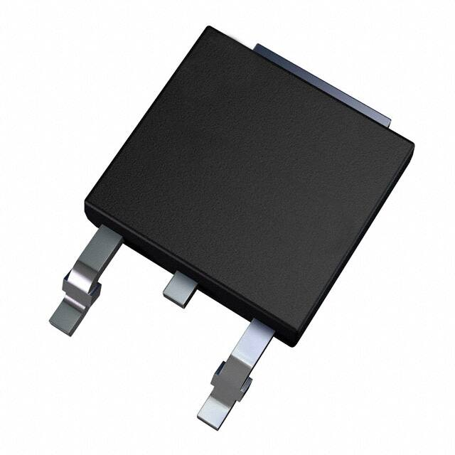
Packages: TO-252, TO-220, and TO-263
SPX1587
3 Pin TO-263
1
2
SPX1587
3
3 Pin TO-220
1
ADJ/GND VOUT
2
3
VIN
ADJ/GND VOUT VIN
APPLICATIONS
■
■
■
■
■
■
■
Desktop PC's Servers
Powering VGA and Sound Cards
Cordless Phones
Battery Chargers
Adjustable Power Supplies
Portable Instrumentation
SMPS Post-Regulator
DESCRIPTION
The SPX1587 is a low power positive-voltage regulator designed to satisfy moderate power requirements
with a cost effective, small footprint solution. This device is an excellent choice for use in battery-powered
applications and portable computers. The SPX1587 features very low quiescent current and a low dropout
voltage of 1.1V at a full load. As output current decreases, quiescent current flows into the load, increasing
efficiency. SPX1587 is available in adjustable or fixed 1.5V, 1.8V, 2.5V, 3.3V and 5.0V output voltages.
The SPX1587 is offered in several 3-pin surface mount packages: TO-252, TO-220 and TO-263. An output
capacitor of 10µF ceramic or tantalum provides unconditional stability.
FUNCTIONAL DIAGRAM (Adjustable)
VIN
+
Current Limit
VOUT
ICL
VREF
+
–
Jun8-07 Rev D
ADJ/GND
I TL
SPX1587 Low-Dropout Voltage Regulator
�
IADJ ~ 50µA
–
Thermal Limit
_
AMP
+ 1.25V
© 2007 Sipex Corporation
�ABSOLUTE MAXIMUM RATINGS
Operating Junction Temperature Range.....-40°C to +125°C
Input Supply Voltage .................................................... +10V
Input to Output Voltage ................................................ +8.8V
ESD Rating .............................................................. 2kV min
Power Dissipation.......................................Internally Limited
Lead Temperature (soldering, 5 seconds) ................ 260°C
Storage Temperature Range.......................-65°C to +150°C
ELECTRICAL CHARACTERISTICS
Specifications are at VIN=VOUT + 1.5V, TA = 25°C, CIN = COUT = 10µF, IOUT =10mA, unless otherwise specified. The z denotes
the specifications which apply full operating temperature range -40°C to +85°C, unless otherwise specified.
PARAMETER
MIN
1.5V Version
Output Voltage
TYP
MAX
MIN
SPX1587A
TYP
MAX
UNITS
CONDITIONS
SPX1587
1.485
1.470
1.500
1.515
1.530
1.470
1.455
1.500
1.530
1.545
V
1.782
1.764
1.800
1.818
1.836
1.764
1.746
1.800
1.836
1.854
V
2.475
2.450
2.500
2.525
2.550
2.450
2.425
2.500
2.550
2.575
V
3.267
3.234
3.300
3.333
3.366
3.234
3.201
3.300
3.366
3.399
V
4.950
4.900
5.000
5.050
5.100
4.900
4.850
5.000
5.100
5.150
V
1.238
1.225
1.250
1.262
1.275
1.225
1.212
1.250
1.275
1.287
V
z
IOUT = 10mA, VIN =3.5V
10mA )I OUT ) 3A, 3.0V )V IN ) 10V
z
IOUT = 10mA, VIN =3.8V
10mA )I OUT ) 3A, 3.3V )V IN ) 10V
z
IOUT = 10mA, VIN =4.5V
10mA )I OUT ) 3A, 4.25V )V IN ) 10V
z
IOUT = 10mA, VIN =5V
10mA )I OUT ) 3A, 4.75V )V IN ) 10V
z
IOUT=10mA, VIN=7V
10mA )I OUT ) 3A, 6.50V )V IN ) 10V
z
IOUT=10mA, (VIN - VOUT )= 2V
10mA)IOUT) 3A, 1.5V)(VIN-VOUT)) 10V
1.8V Version
Output Voltage
2.5V Version
Output Voltage
3.3V Version
Output Voltage
5.0V Version
Output Voltage
All Voltage Options
Reference Voltage
Output Voltage
Temperature Stability
0.3
Line Regulation
0.1
0.1
0.1
0.1
0.1
0.2
0.2
0.2
0.2
0.2
0.1
0.1
0.1
0.1
0.1
0.2
0.2
0.2
0.2
0.2
%
3.0V)VIN) 10V,VOUT=1.5V
3.3V)VIN) 10V,VOUT=1.8V
4.25V)VIN) 10V,VOUT=2.5V
4.75V)VIN) 10V,VOUT=3.3V
6.50V)VIN) 10V,VOUT=5.0V
Load Regulation
0.1
0.1
0.1
0.1
0.1
0.3
0.3
0.3
0.3
0.3
0.1
0.1
0.1
0.1
0.1
0.3
0.3
0.3
0.3
0.3
%
10mA)IOUT) 3A, VOUT=1.5V
10mA)IOUT) 3A, VOUT=1.8V
10mA)IOUT) 3A, VOUT=2.5V
10mA)IOUT) 3A, VOUT=3.3V
10mA)IOUT) 3A, VOUT=5.0V
Dropout Voltage
(Note 2)
1.00
1.05
1.10
V
1.2
1.00
1.05
1.10
1.2
IOUT=1A
IOUT=2A
IOUT=3A
4
10
4
10
mA
Quiescent Current
4
10
4
10
mA
Adjust Pin Current
50
Minimum Load Current
(Note 4)
Current Limit
3.2
Thermal Regulation
Ripple Rejection
75
50
120
5
0.01
60
0.5
3.2
0.1
75
Fixed voltage versions
µA
120
5
0.01
60
%
z
A
0.1
%/W
dB
(VIN-VOUT)=2V
25°C, 30mS pulse
FRIPPLE=120Hz, (VIN-VOUT)=2V,
VRIPPLE=1VPP
Long Term Stability
0.03
0.03
%
125°C, 1000Hrs
RMS Output Noise
0.003
0.003
%
% of VOUT, 10Hz)f)10kHz
Thermal Resistance
3
29.4
3
31.4
6
50
3
29.4
3
31.4
6
50
°C/W
Jun8-07 Rev D
SPX1587 Low-Dropout Voltage Regulator
�
TO-220 Junction to Case, at Tab
TO-220 Junction to Ambient
TO-263 Junction to Case, at Tab
TO-263 Junction to Ambient
TO-252 Junction to Case, at Tab
TO-252 Junction to Ambient
© 2007 Sipex Corporation
�ELECTRICAL CHARACTERISTICS: Continued (Notes)
NOTES:
Note 1: Output temperature coefficient is defined as the worst case voltage change divided by the total temperature range
Note 2: Dropout voltage is defined as the input to output differential at which the output voltage drops 100mV below its nominal value
measured at 1V differential at very low values of programmed output voltage, the minimum input supply voltage of 2V ( 2.3V
over temperature) must be taken into account.
Note 3: Thermal regulation is defined as the change in output voltage at a time T after a change in power dissipation is applied. excluding
load or line regulation effect.
Note 4: Adjustable Version Only.
TYPICAL PERFORMANCE CHARACTERISTICS
3.325
1.275
3.320
1.265
1.25v Adj
1.27
Vout (V)
Vout (V)
1.26
3.315
3.310
1.255
1.25
1.245
1.24
3.305
1.235
1.23
3.300
4.5
6.5
8.5
10.5
12.5
1.225
-50
14.5
Vin (V)
Figure 1. Line Regulation for SPX1587U-3.3; IOUT=10mA
-10
10
30
50
70
Temp (C)
90
110
130
Figure 2. VOUTvs Temperature, V IN=2.5V, IOUT=10mA
3.38
2.55
2.5v Adj
2.5v Fixed
2.54
3.3v Adj
3.3v Fixed
3.36
2.53
Vout (V)
2.52
Vout (V)
-30
2.51
2.5
2.49
3.34
3.32
3.3
2.48
2.47
3.28
2.46
2.45
-50
-30
-10
10
30
50
70
90
3.26
-50
110 130
-30
Temp (°C)
10
30
50
70
90
110 130
Temp (C)
Figure 4. VIN=5.0V, IOUT=10mA
Figure 3. VIN=4.0V, IOUT=10mA
Jun8-07 Rev D
-10
SPX1587 Low-Dropout Voltage Regulator
�
© 2007 Sipex Corporation
�APPLICATION INFORMATION
Output Capacitor
However the value of the ADJ-bypass capacitor
should be chosen with respect to the following
equation:
C = 1 / ( 6.28 * FR* R 1)
Where
C = value of the capacitor in Farads
(select an equal or larger standard value),
FR= ripple frequency in Hz,
R1= value of resistor R1 in Ohms.
To ensure the stability of the SPX1587, an output
capacitor of at least 10µF (ceramic or tantalum) or
22µF (aluminum) is required. The value may change
based on the application requirements of the output
load or temperature range. The value of ESR can vary
based on the type of capacitor used in the applications to guarantee stability. The recommended value
for ESR is 0.51 or less. A larger value of output
capacitance (up to 100µF) can improve the load
transient response.
If an ADJ-bypass capacitor is used, the amplitude of
the output ripple will be independent of the output
voltage. If an ADJ-bypass capacitor is not used, the
output ripple will be proportional to the ratio of the
output voltage to the reference voltage:
M = VOUT / VREF
Soldering Methods
The SPX1587 die is attached to the heatsink lead which
exits opposite the input, output, and ground pins.
Thermal Characteristics
Where M = multiplier for the ripple seen when the
ADJ pin is optimally bypassed.
The SPX1587 features the internal thermal limiting
to protect the device during overload conditions.
Special care needs to be taken during continuous load
conditions such that the maximum junction temperature does not exceed 125°C. Thermal protection is
activated at >179°C and deactiviated at


 工商网监
湘ICP备2023018690号
工商网监
湘ICP备2023018690号
