Advanced Science And Novel Technology Company, Inc.
2790 Skypark Drive Suite 112, Torrance, CA 90505
Offices: 310-530-9400 / Fax: 310-530-9402
www.adsantec.com
ASNT1124-KMM
DC-64Gbps Broadband Digital DDR 4:1 Multiplexer
Ideal for high speed proof-of-concept prototyping
Differential CML I/O data and clock buffers
Differential duty cycle adjustment control for input clock
SE amplitude adjustment control for output data
Half-rate clock input (DDR mode)
Quarter-rate clock output
Single +3.3V or -3.3V power supply
Power consumption: 1.18W
Fabricated in SiGe for high performance, yield, and reliability
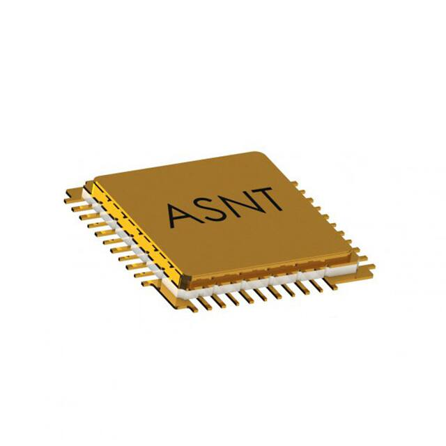
Custom CQFP 44-pin package
vcc
vee
vcc
d1p
vcc
d1n
vcc
vcc
ampadj
vcc
qp
ASNT1124-KMM
d2p
vcc
d2n
vcc
vcc
qn
vcc
1
cep
vcc
cen
vcc
vcc
d3n
vcc
dccp
vcc
dccn
vcc
vcc
vee
vcc
d3p
Rev. 1.2.2
vee
vcc
Exhibits low jitter and limited temperature variation over industrial temperature range
vcc
c4op
vcc
d0n
vcc
d0p
vcc
c4on
High speed broadband 4:1 Multiplexer (MUX)
vcc
May 2020
�Advanced Science And Novel Technology Company, Inc.
2790 Skypark Drive Suite 112, Torrance, CA 90505
Offices: 310-530-9400 / Fax: 310-530-9402
www.adsantec.com
DESCRIPTION
vcc 50 Ohm
d0p
d0n
ampadj
50 Ohm vccо
d1p
d1n
qp
qn
d2p
d2n
50 Ohm
d3p
d3n
50 Ohm
cep
cen
c4op
c4on
DIV
50 Ohm
50 Ohm
dccp
dccn
vcc
1000 Ohm
Fig. 1. Functional Block Diagram
The ASNT1124-KMM SiGe IC is a low power and high-speed digital 4 to 1 serializer-multiplexer
(MUX) that functions seamlessly over data rates (fbit) ranging from DC to its maximum frequency.
The main function of the part shown in Fig. 1 is to multiplex 4 parallel differential CML data signals
d0p/d0n, d1p/d1n, d2p/d2n, d3p/d3n running at a bit rate of fbit/4 into a high speed serial bit stream
qp/qn running at a bit rate of fbit. Differential or single-ended half-rate clock cep/cen (DDR mode) must
be provided by an external source for the part to function properly.
The serialized data words qp/qn and the clock divided-by-4 signal c4op/c4on are transmitted through
CML output interfaces. The clock and data outputs are phase-matched to each other resulting in very little
relative skew over the operating temperature range of the device.
The part’s I/O’s support the CML logic interface with on chip 50Ohm termination to vcc and may be used
differentially, AC/DC coupled, single-ended, or in any combination (see also POWER SUPPLY
CONFIGURATION). In the DC-coupling mode, the input signal’s common mode voltage should comply
with the specifications shown in ELECTRICAL CHARACTERISTICS. In the AC-coupling mode, the
input termination provides the required common mode voltage automatically. The differential DC
signaling mode is recommended for optimal performance.
Rev. 1.2.2
2
May 2020
�Advanced Science And Novel Technology Company, Inc.
2790 Skypark Drive Suite 112, Torrance, CA 90505
Offices: 310-530-9400 / Fax: 310-530-9402
www.adsantec.com
Output Amplitude Adjustment Port
The output amplitude is controlled through a SE tuning port ampadj. The simulated dependence of the
output amplitude vs. the control voltage is shown in Fig. 2. The ampadj control signal should not be set
higher than the default value of vcc – 0.66V (see Electrical Characteristics table for allowable range.)
Fig. 2. Simulated Output Amplitude vs. Control Voltage Diagram
Input Clock Duty Cycle Adjustment Port
In AC coupled mode of operation duty cycle of the input clock signal can be adjusted via a pair of DC
analog tuning ports dccp and dccn. By lowering the voltage of one of the ports below vcc while keeping
the other one at vcc or not connected the common mode voltage of the corresponding clock input can be
lowered below vcc. If both control inputs are left not connected the common mode voltages of both clock
inputs are at vcc. The dependence of either input clock common mode voltage on the control voltage is
shown in Fig. 3.
Fig. 3. Dependence of cep (or cen) Common Mode Voltage on dccp (or dccn) Voltage
Rev. 1.2.2
3
May 2020
�Advanced Science And Novel Technology Company, Inc.
2790 Skypark Drive Suite 112, Torrance, CA 90505
Offices: 310-530-9400 / Fax: 310-530-9402
www.adsantec.com
POWER SUPPLY CONFIGURATION
The part can operate with either negative supply (vcc = 0.0V = ground and vee = −3.3V), or positive
supply (vcc = +3.3V and vee = 0.0V = ground). In case of the positive supply, all I/Os need AC
termination when connected to any devices with 50Ohm termination to ground. Different PCB layouts
will be needed for each different power supply combination.
All the characteristics detailed below assume vcc = 0.0V and vee = -3.3V.
ABSOLUTE MAXIMUM RATINGS
Caution: Exceeding the absolute maximum ratings shown in Table 1 may cause damage to this product
and/or lead to reduced reliability. Functional performance is specified over the recommended operating
conditions for power supply and temperature only. AC and DC device characteristics at or beyond the
absolute maximum ratings are not assumed or implied. All min and max voltage limits are referenced to
ground.
Table 1. Absolute Maximum Ratings
Parameter
Supply Voltage (vee)
Power Consumption
RF Input Voltage Swing (SE)
Case Temperature
Storage Temperature
Operational Humidity
Storage Humidity
Rev. 1.2.2
Min
-40
10
10
4
Max
-3.6
1.3
1.4
+90
+100
98
98
Units
V
W
V
ºC
ºC
%
%
May 2020
�Advanced Science And Novel Technology Company, Inc.
2790 Skypark Drive Suite 112, Torrance, CA 90505
Offices: 310-530-9400 / Fax: 310-530-9402
www.adsantec.com
TERMINAL FUNCTIONS
TERMINAL
Name
No.
Type
d0p
d0n
d1p
d1n
d2p
d2n
d3p
d3n
c4op
c4on
ampadj
dccp
dccn
cep
cen
qp
qn
Name
vcc
vee
Rev. 1.2.2
DESCRIPTION
Low-Speed I/Os
30
CML Differential quarter-rate data inputs with internal SE 50Ohm
input termination to vcc
32
37
CML Differential quarter-rate data inputs with internal SE 50Ohm
input termination to vcc
39
41
CML Differential quarter-rate data inputs with internal SE 50Ohm
input termination to vcc
43
4
CML Differential quarter-rate data inputs with internal SE 50Ohm
input termination to vcc
6
26
CML Differential quater-rate clock outputs with internal SE 50Ohm
output termination to vcc. Require external SE 50Ohm termination to vcc
28
Analog DC Control Inputs
21
Analog SE tuning port terminated to internal resistive divider between vee
input and vcc.
15
Analog Differential or SE tuning ports with internal SE connections to
inputs dp/dn through 1000Ohm resistors.
13
High-Speed I/Os
8
CML Differential half-rate clock input signals with internal 50Ohm
input termination to vcc
10
19
CML Differential full-rate data outputs with internal SE 50Ohm
output termination to vcc. Require external SE 50Ohm termination to vcc
17
Supply and Termination Voltages
Description
Pin Number
Positive power supply
1, 3, 5, 7, 9, 11, 12, 14, 16, 18, 20, 22, 23, 25, 27, 29,
(+3.3V or 0)
31, 33, 34, 36, 38, 40, 42, 44
Negative power supply
2, 24, 35
(0V or -3.3V)
5
May 2020
�Advanced Science And Novel Technology Company, Inc.
2790 Skypark Drive Suite 112, Torrance, CA 90505
Offices: 310-530-9400 / Fax: 310-530-9402
www.adsantec.com
ELECTRICAL CHARACTERISTICS
PARAMETER
MIN
TYP MAX
UNIT
COMMENTS
General Parameters
-3.1
-3.3
-3.5
V
±6%
vee
0.0
V
External ground
vcc
Ivee
358
mA
Power consumption
1180
mW
Junction temperature
-40
25
125
°C
LS Input Data (d0p/d0n, d1p/d1n, d2p/d2n, d3p/d3n)
Data Rate
DC
10
16
Gb/s
Swing
0.2
0.8
V
Differential or SE, p-p
CM Voltage Level
vcc-0.8
vcc
V
Must match for both inputs
HS Input Clock (cep/cen)
Frequency
DC
20
32
GHz
Swing
0.2
0.8
V
Differential or SE, p-p
CM Voltage Level
vcc-0.8
vcc
V
Must match for both inputs
Duty Cycle
40
50
60
%
DC Tuning port (dccp/dccn)
Control voltage range
vee
vcc
DC Tuning port (ampadj)
Control voltage range vcc-1.4
vcc-0.66
V
Default voltage is vcc-0.66V
HS Output Data (qp/qn)
Data Rate
DC
40
64
Gb/s
Logic “1” level
V
vcc
Logic “0” level
vcc-0.4
V
With external 50Ohm DC termination
Output Jitter
2
ps
Peak-to-peak at 40Gb/s
LS Output Clock (c4op/c4on)
Frequency
DC
10
16
GHz
Logic “1” level
V
vcc
Logic “0” level
vcc-0.4
V
With external 50Ohm DC termination
Duty Cycle
50
%
Output Jitter
1
ps
Peak-to-peak at 10GHz
PACKAGE INFORMATION
The chip die is housed in a custom 44-pin CQFP package shown in Fig. 4. The package provides a center
heat slug located on its back side to be used for heat dissipation. ADSANTEC recommends for this
section to be soldered to the vcc plain, which is ground for a negative supply, or power for a positive
supply.
The part’s identification label is ASNT1124-KMM. The first 8 characters of the name before the dash
identify the bare die including general circuit family, fabrication technology, specific circuit type, and part
Rev. 1.2.2
6
May 2020
�Advanced Science And Novel Technology Company, Inc.
2790 Skypark Drive Suite 112, Torrance, CA 90505
Offices: 310-530-9400 / Fax: 310-530-9402
www.adsantec.com
version while the 3 characters after the dash represent the package’s manufacturer, type, and pin out
count.
The IC complies with the Restriction of Hazardous Substances (RoHS) per 2011/65/EU for all ten
substances.
Fig. 4. CQFP 44-Pin Package Drawing (All Dimensions in mm)
Rev. 1.2.2
7
May 2020
�Advanced Science And Novel Technology Company, Inc.
2790 Skypark Drive Suite 112, Torrance, CA 90505
Offices: 310-530-9400 / Fax: 310-530-9402
www.adsantec.com
REVISION HISTORY
Revision
1.2.2
1.1.2
1.1.1
Date
05-2020
07-2019
07-2015
1.0.1
1.0.0
05-2015
09-2014
Rev. 1.2.2
Changes
Updated Package Information
Updated Letterhead
Correction of the duty cycle control function description including:
- block diagram
- pinout diagram
- part description
- terminal functions
Corrected power consumption and current consumption
Modified maximum voltage value on DC tuning port ampadj
First release
Preliminary release
8
May 2020
�