MC10H176
Hex D Master‐Slave
Flip‐Flop
Description
The MC10H176 contains six master slave type D flip-flops with a
common clock. This MECL 10H™ part is a functional/pinout
duplication of the standard MECL 10K™ family part, with 100%
improvement in clock frequency and propagation delay and no
increase in power-supply current.
www.onsemi.com
Features
• Propagation Delay, 1.7 ns Typical
• Power Dissipation, 460 mW Typical
• Improved Noise Margin 150 mV (Over Operating Voltage and
16
1
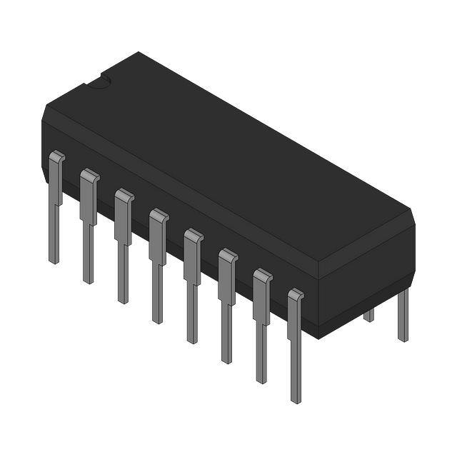
PDIP−16
P SUFFIX
CASE 648−02
Temperature Range)
• Voltage Compensated
• MECL 10K Compatible
• These Devices are Pb-Free, Halogen Free and are RoHS Compliant
MARKING DIAGRAMS*
CLOCKED TRUTH TABLE
C
Q
Qn+1
L
X
Qn
H*
L
L
H*
H
H
16
MC10H176P
AWLYYWWG
1
* A clock H is a clock transition from
a low to a high state.
A
WL, L
YY, Y
WW, W
G
DIP
PIN ASSIGNMENT
VCC1
1
16
VCC2
Q0
2
15
Q5
Q1
3
14
Q4
Q2
4
13
Q3
D0
5
12
D5
D1
6
11
D4
D2
7
10
D3
VEE
8
9
CLOCK
= Assembly Location
= Wafer Lot
= Year
= Work Week
= Pb-Free Package
*For additional marking information, refer to
Application Note AND8002/D.
ORDERING INFORMATION
Device
MC10H176PG
Package
Shipping
PDIP−16
(Pb-Free)
25 Units/Tube
Pin assignment is for Dual−in−Line Package.
For PLCC pin assignment, see the Pin Conversion Tables on page 18
of the ON Semiconductor MECL Data Book (DL122/D).
© Semiconductor Components Industries, LLC, 2016
August, 2016 − Rev. 8
1
Publication Order Number:
MC10H176/D
�MC10H176
Table 1. MAXIMUM RATINGS
Symbol
Rating
Unit
VEE
Power Supply (VCC = 0)
Characteristic
−8.0 to 0
Vdc
VI
Input Voltage (VCC = 0)
0 to VEE
Vdc
Iout
Output Current
Continuous
Surge
TA
Operating Temperature Range
Tstg
Storage Temperature Range
Plastic
Ceramic
mA
50
100
0 to +75
°C
°C
−55 to +150
−55 to +165
Table 2. ELECTRICAL CHARACTERISTICS (VEE = −5.2 V ±5%) (Note 1)
0°
Symbol
Characteristic
25°
75°
Min
Max
Min
Max
Min
Max
Unit
mA
IE
Power Supply Current
−
123
−
112
−
123
IinH
Input Current High
Pins 5,6,7,10,11,12
Pin 9
−
−
425
670
−
−
265
420
−
−
265
420
IinL
Input Current Low
0.5
−
0.5
−
0.3
−
mA
VOH
High Output Voltage
−1.02
−0.84
−0.98
−0.81
−0.92
−0.735
Vdc
VOL
Low Output Voltage
−1.95
−1.63
−1.95
−1.63
−1.95
−1.60
Vdc
VIH
High Input Voltage
−1.17
−0.84
−1.13
−0.81
−1.07
−0.735
Vdc
VIL
Low Input Voltage
−1.95
−1.48
−1.95
−1.48
−1.95
−1.45
Vdc
mA
1. Each MECL 10H™ series circuit has been designed to meet the dc specifications shown in the test table, after thermal equilibrium has
been established. The circuit is in a test socket or mounted on a printed circuit board and transverse air flow greater than 500 linear fpm
is maintained. Outputs are terminated through a 50 W resistor to −2.0 V.
Table 3. AC PARAMETERS
tpd
Propagation Delay
0.9
2.1
0.9
2.2
1.0
2.4
ns
tset
Set-up Time
1.5
−
1.5
−
1.5
−
ns
thold
Hold Time
0.9
−
0.9
−
1.0
−
ns
tr
Rise Time
0.5
1.8
0.5
1.9
0.5
2.0
ns
tf
Fall Time
0.5
1.8
0.5
1.9
0.5
2.0
ns
Toggle Frequency
250
−
250
−
250
−
MHz
ftog
NOTE: Device will meet the specifications after thermal equilibrium has been established when mounted in a test socket or printed circuit
board with maintained transverse airflow greater than 500 lfpm. Electrical parameters are guaranteed only over the declared
operating temperature range. Functional operation of the device exceeding these conditions is not implied. Device specification limit
values are applied individually under normal operating conditions and not valid simultaneously.
www.onsemi.com
2
�MC10H176
APPLICATION INFORMATION
The MC10H176 contains six high-speed, master slave
type “D” flip-flops. Data is entered into the master when the
clock is low. Master-to-slave data transfer takes place on the
positive-going Clock transition. Thus, outputs may change
only on a positive-going Clock transition. A change in the
information present at the data (D) input will not affect the
output information any other time due to the master-slave
construction of this device.
LOGIC DIAGRAM
D0
5
2
Q0
D1
6
3
Q1
D2
7
4
Q2
D3
10
13
Q3
VCC1 = PIN 1
VCC2 = PIN 16
VEE = PIN 8
D4
11
14
Q4
D5
12
15
Q5
CLOCK
9
www.onsemi.com
3
�MC10H176
PACKAGE DIMENSIONS
PDIP−16
CASE 648−08
ISSUE V
D
A
16
9
E
H
E1
1
NOTE 8
b2
8
c
B
TOP VIEW
END VIEW
WITH LEADS CONSTRAINED
NOTE 5
A2
A
e/2
NOTE 3
L
A1
C
D1
e
SEATING
PLANE
M
eB
END VIEW
16X b
SIDE VIEW
0.010
M
C A
M
B
M
STYLE 1:
PIN 1. CATHODE
2. CATHODE
3. CATHODE
4. CATHODE
5. CATHODE
6. CATHODE
7. CATHODE
8. CATHODE
9. ANODE
10. ANODE
11. ANODE
12. ANODE
13. ANODE
14. ANODE
15. ANODE
16. ANODE
NOTE 6
NOTES:
1. DIMENSIONING AND TOLERANCING PER ASME Y14.5M, 1994.
2. CONTROLLING DIMENSION: INCHES.
3. DIMENSIONS A, A1 AND L ARE MEASURED WITH THE PACKAGE SEATED IN JEDEC SEATING PLANE GAUGE GS−3.
4. DIMENSIONS D, D1 AND E1 DO NOT INCLUDE MOLD FLASH
OR PROTRUSIONS. MOLD FLASH OR PROTRUSIONS ARE
NOT TO EXCEED 0.10 INCH.
5. DIMENSION E IS MEASURED AT A POINT 0.015 BELOW DATUM
PLANE H WITH THE LEADS CONSTRAINED PERPENDICULAR
TO DATUM C.
6. DIMENSION eB IS MEASURED AT THE LEAD TIPS WITH THE
LEADS UNCONSTRAINED.
7. DATUM PLANE H IS COINCIDENT WITH THE BOTTOM OF THE
LEADS, WHERE THE LEADS EXIT THE BODY.
8. PACKAGE CONTOUR IS OPTIONAL (ROUNDED OR SQUARE
CORNERS).
DIM
A
A1
A2
b
b2
C
D
D1
E
E1
e
eB
L
M
INCHES
MIN
MAX
−−−−
0.210
0.015
−−−−
0.115 0.195
0.014 0.022
0.060 TYP
0.008 0.014
0.735 0.775
0.005
−−−−
0.300 0.325
0.240 0.280
0.100 BSC
−−−−
0.430
0.115 0.150
−−−−
10 °
MILLIMETERS
MIN
MAX
−−−
5.33
0.38
−−−
2.92
4.95
0.35
0.56
1.52 TYP
0.20
0.36
18.67 19.69
0.13
−−−
7.62
8.26
6.10
7.11
2.54 BSC
−−−
10.92
2.92
3.81
−−−
10 °
STYLE 2:
PIN 1. COMMON DRAIN
2. COMMON DRAIN
3. COMMON DRAIN
4. COMMON DRAIN
5. COMMON DRAIN
6. COMMON DRAIN
7. COMMON DRAIN
8. COMMON DRAIN
9. GATE
10. SOURCE
11. GATE
12. SOURCE
13. GATE
14. SOURCE
15. GATE
16. SOURCE
MECL is a trademark of Semiconductor Components Industries, LLC (SCILLC) or its subsidiaries in the United States and/or other countries.
ON Semiconductor and
are trademarks of Semiconductor Components Industries, LLC dba ON Semiconductor or its subsidiaries in the United States and/or other countries.
ON Semiconductor owns the rights to a number of patents, trademarks, copyrights, trade secrets, and other intellectual property. A listing of ON Semiconductor’s product/patent
coverage may be accessed at www.onsemi.com/site/pdf/Patent-Marking.pdf. ON Semiconductor reserves the right to make changes without further notice to any products herein.
ON Semiconductor makes no warranty, representation or guarantee regarding the suitability of its products for any particular purpose, nor does ON Semiconductor assume any liability
arising out of the application or use of any product or circuit, and specifically disclaims any and all liability, including without limitation special, consequential or incidental damages.
Buyer is responsible for its products and applications using ON Semiconductor products, including compliance with all laws, regulations and safety requirements or standards,
regardless of any support or applications information provided by ON Semiconductor. “Typical” parameters which may be provided in ON Semiconductor data sheets and/or
specifications can and do vary in different applications and actual performance may vary over time. All operating parameters, including “Typicals” must be validated for each customer
application by customer’s technical experts. ON Semiconductor does not convey any license under its patent rights nor the rights of others. ON Semiconductor products are not
designed, intended, or authorized for use as a critical component in life support systems or any FDA Class 3 medical devices or medical devices with a same or similar classification
in a foreign jurisdiction or any devices intended for implantation in the human body. Should Buyer purchase or use ON Semiconductor products for any such unintended or unauthorized
application, Buyer shall indemnify and hold ON Semiconductor and its officers, employees, subsidiaries, affiliates, and distributors harmless against all claims, costs, damages, and
expenses, and reasonable attorney fees arising out of, directly or indirectly, any claim of personal injury or death associated with such unintended or unauthorized use, even if such
claim alleges that ON Semiconductor was negligent regarding the design or manufacture of the part. ON Semiconductor is an Equal Opportunity/Affirmative Action Employer. This
literature is subject to all applicable copyright laws and is not for resale in any manner.
PUBLICATION ORDERING INFORMATION
LITERATURE FULFILLMENT:
Literature Distribution Center for ON Semiconductor
19521 E. 32nd Pkwy, Aurora, Colorado 80011 USA
Phone: 303−675−2175 or 800−344−3860 Toll Free USA/Canada
Fax: 303−675−2176 or 800−344−3867 Toll Free USA/Canada
Email: orderlit@onsemi.com
N. American Technical Support: 800−282−9855 Toll Free
USA/Canada
Europe, Middle East and Africa Technical Support:
Phone: 421 33 790 2910
Japan Customer Focus Center
Phone: 81−3−5817−1050
www.onsemi.com
4
ON Semiconductor Website: www.onsemi.com
Order Literature: http://www.onsemi.com/orderlit
For additional information, please contact your local
Sales Representative
MC10H176/D
�


 工商网监
湘ICP备2023018690号
工商网监
湘ICP备2023018690号
