MC9S08GB60
MC9S08GB32
MC9S08GT60
MC9S08GT32
MC9S08GT16
Technical Data
HCS08
Microcontrollers
MC9S08GB60/D
Rev. 2.1, 4/2004
WWW.MOTOROLA.COM/SEMICONDUCTORS
��DOCUMENT NUMBER
MC9S08GB60/D
MC9S08GB/GT
Data Sheet
V2.1
8-/16-Bit Products Division
Motorola, Inc.
Motorola reserves the right to make changes without further notice to any products herein. Motorola makes no warranty, representation or guarantee regarding the suitability of its
products for any particular purpose, nor does Motorola assume any liability arising out of the application or use of any product or circuit, and specifically disclaims any and all liability,
including without limitation consequential or incidental damages. “Typical” parameters which may be provided in Motorola data sheets and/or specifications can and do vary in
different applications and actual performance may vary over time. All operating parameters, including “Typicals” must be validated for each customer application by customer’s
technical experts. Motorola does not convey any license under its patent rights nor the rights of others. Motorola products are not designed, intended, or authorized for use as
components in systems intended for surgical implant into the body, or other applications intended to support or sustain life, or for any other application in which the failure of the
Motorola product could create a situation where personal injury or death may occur. Should Buyer purchase or use Motorola products for any such unintended or unauthorized
application, Buyer shall indemnify and hold Motorola and its officers, employees, subsidiaries, affiliates, and distributors harmless against all claims, costs, damages, and expenses,
and reasonable attorney fees arising out of, directly or indirectly, any claim of personal injury or death associated with such unintended or unauthorized use, even if such claim alleges
that Motorola was negligent regarding the design or manufacture of the part. Motorola and
are registered trademarks of Motorola, Inc. Motorola, Inc. is an Equal
Opportunity/Affirmative Action Employer.
©Motorola, Inc., 2003, 2004
MOTOROLA
MC9S08GB/GT
3
�Revision History
To provide the most up-to-date information, the revision of our documents on the World Wide Web will
be the most current. Your printed copy may be an earlier revision. To verify you have the latest information
available, refer to:
http://motorola.com/semiconductors
The following revision history table summarizes changes contained in this document.
Revision
Number
Revision
Date
1.0
4/25/2003
Description of Changes
Initial release
1.1
Electricals change, appendix A only
1.2
Electricals change, appendix A only
1.3
10/2/2003
Added module version table; clarifications
1.4
10/29/2003
Fixed typos and made corrections and
clarifications
1.5
11/12/2003
Added 1-MHz IDD values to Electricals,
appendix A
2
2/10/2004
Changed format of register names to enable
reuse of code (from SCIBD to SCI1BD, even
when only one instance of a module on a chip)
Added new device: MC9S08GT16 to book.
Added new 48-pin QFN package to book.
BKGDPE description in Section 5 — changed
PTD0 to PTG0. Changed typo in CPU section
that listed MOV instruction as being 6 cycles
instead of 5 (Table 7-2).
2.1
4/21/2004
ICG, added Fixed Frequency Clock section.
TPM, added reference to new ICG section.
This product incorporates SuperFlash technology licensed from SST.
Motorola and the Stylized M Logo are registered trademarks of Motorola, Inc.
DigitalDNA is a trademark of Motorola, Inc.
4
MC9S08GB/GT
Motorola, Inc., 2003, 2004
MOTOROLA
�Data Sheet — MC9S08GB60/D V2.1
List of Sections
Section 1 Introduction. . . . . . . . . . . . . . . . . . . . . . . . . . . . . . . . . . . . . . . . . . . . 17
Section 2 Pins and Connections . . . . . . . . . . . . . . . . . . . . . . . . . . . . . . . . . . . 23
Section 3 Modes of Operation . . . . . . . . . . . . . . . . . . . . . . . . . . . . . . . . . . . . . 33
Section 4 Memory . . . . . . . . . . . . . . . . . . . . . . . . . . . . . . . . . . . . . . . . . . . . . . . 41
Section 5 Resets, Interrupts, and System Configuration . . . . . . . . . . . . . . . 63
Section 6 Internal Clock Generator (ICG) Module . . . . . . . . . . . . . . . . . . . . . 81
Section 7 Central Processor Unit (CPU) . . . . . . . . . . . . . . . . . . . . . . . . . . . . 109
Section 8 Parallel Input/Output . . . . . . . . . . . . . . . . . . . . . . . . . . . . . . . . . . . 129
Section 9 Keyboard Interrupt (KBI) Module . . . . . . . . . . . . . . . . . . . . . . . . . 149
Section 10 Timer/PWM (TPM) Module . . . . . . . . . . . . . . . . . . . . . . . . . . . . . . 155
Section 11 Serial Communications Interface (SCI) Module. . . . . . . . . . . . . 171
Section 12 Serial Peripheral Interface (SPI) Module . . . . . . . . . . . . . . . . . . 191
Section 13 Inter-Integrated Circuit (IIC) Module . . . . . . . . . . . . . . . . . . . . . . 207
Section 14 Analog-to-Digital Converter (ATD) Module . . . . . . . . . . . . . . . . 221
Section 15 Development Support . . . . . . . . . . . . . . . . . . . . . . . . . . . . . . . . . 237
Appendix A Electrical Characteristics. . . . . . . . . . . . . . . . . . . . . . . . . . . . . . 261
Appendix B Ordering Information and Mechanical Drawings. . . . . . . . . . . 283
MOTOROLA
MC9S08GB/GT
5
�List of Sections
6
MC9S08GB/GT
MOTOROLA
�Data Sheet — MC9S08GB60/D V2.1
Table of Contents
Section 1 Introduction
1.1
1.2
1.2.1
1.2.2
1.2.3
1.3
1.4
Overview. . . . . . . . . . . . . . . . . . . . . . . . . . . . . . . . . . . . . . . . . . . . . . . . . . . . . . . . . . 17
Features . . . . . . . . . . . . . . . . . . . . . . . . . . . . . . . . . . . . . . . . . . . . . . . . . . . . . . . . . . 17
Standard Features of the HCS08 Family . . . . . . . . . . . . . . . . . . . . . . . . . . . . . . . 17
Features of MC9S08GB/GT Series of MCUs. . . . . . . . . . . . . . . . . . . . . . . . . . . . 17
Devices in the MC9S08GB/GT Series . . . . . . . . . . . . . . . . . . . . . . . . . . . . . . . . . 18
MCU Block Diagrams . . . . . . . . . . . . . . . . . . . . . . . . . . . . . . . . . . . . . . . . . . . . . . . . 19
System Clock Distribution. . . . . . . . . . . . . . . . . . . . . . . . . . . . . . . . . . . . . . . . . . . . . 21
Section 2 Pins and Connections
2.1
Introduction. . . . . . . . . . . . . . . . . . . . . . . . . . . . . . . . . . . . . . . . . . . . . . . . . . . . . . . . 23
2.2
Device Pin Assignment. . . . . . . . . . . . . . . . . . . . . . . . . . . . . . . . . . . . . . . . . . . . . . . 23
2.3
Recommended System Connections . . . . . . . . . . . . . . . . . . . . . . . . . . . . . . . . . . . . 26
2.3.1
Power . . . . . . . . . . . . . . . . . . . . . . . . . . . . . . . . . . . . . . . . . . . . . . . . . . . . . . . . . . 28
2.3.2
Oscillator . . . . . . . . . . . . . . . . . . . . . . . . . . . . . . . . . . . . . . . . . . . . . . . . . . . . . . . 28
2.3.3
Reset . . . . . . . . . . . . . . . . . . . . . . . . . . . . . . . . . . . . . . . . . . . . . . . . . . . . . . . . . . 28
2.3.4
Background/Mode Select (PTG0/BKGD/MS). . . . . . . . . . . . . . . . . . . . . . . . . . . . 29
2.3.5
General-Purpose I/O and Peripheral Ports . . . . . . . . . . . . . . . . . . . . . . . . . . . . . 29
2.3.6
Signal Properties Summary . . . . . . . . . . . . . . . . . . . . . . . . . . . . . . . . . . . . . . . . . 31
Section 3 Modes of Operation
3.1
3.2
3.3
3.4
3.5
3.6
3.6.1
3.6.2
3.6.3
3.6.4
3.6.5
3.6.6
Introduction. . . . . . . . . . . . . . . . . . . . . . . . . . . . . . . . . . . . . . . . . . . . . . . . . . . . . . . . 33
Features . . . . . . . . . . . . . . . . . . . . . . . . . . . . . . . . . . . . . . . . . . . . . . . . . . . . . . . . . . 33
Run Mode . . . . . . . . . . . . . . . . . . . . . . . . . . . . . . . . . . . . . . . . . . . . . . . . . . . . . . . . . 33
Active Background Mode . . . . . . . . . . . . . . . . . . . . . . . . . . . . . . . . . . . . . . . . . . . . . 33
Wait Mode . . . . . . . . . . . . . . . . . . . . . . . . . . . . . . . . . . . . . . . . . . . . . . . . . . . . . . . . 34
Stop Modes . . . . . . . . . . . . . . . . . . . . . . . . . . . . . . . . . . . . . . . . . . . . . . . . . . . . . . . 35
Stop1 Mode . . . . . . . . . . . . . . . . . . . . . . . . . . . . . . . . . . . . . . . . . . . . . . . . . . . . . 35
Stop2 Mode . . . . . . . . . . . . . . . . . . . . . . . . . . . . . . . . . . . . . . . . . . . . . . . . . . . . . 35
Stop3 Mode . . . . . . . . . . . . . . . . . . . . . . . . . . . . . . . . . . . . . . . . . . . . . . . . . . . . . 36
Active BDM Enabled in Stop Mode . . . . . . . . . . . . . . . . . . . . . . . . . . . . . . . . . . . 37
LVD Enabled in Stop Mode . . . . . . . . . . . . . . . . . . . . . . . . . . . . . . . . . . . . . . . . . 37
On-Chip Peripheral Modules in Stop Modes . . . . . . . . . . . . . . . . . . . . . . . . . . . . 38
MOTOROLA
MC9S08GB/GT
7
�Table of Contents
Section 4 Memory
4.1
4.1.1
4.2
4.3
4.4
4.4.1
4.4.2
4.4.3
4.4.4
4.4.5
4.4.6
4.4.7
4.5
4.6
4.6.1
4.6.2
4.6.3
4.6.4
4.6.5
4.6.6
MC9S08GB/GT Memory Map . . . . . . . . . . . . . . . . . . . . . . . . . . . . . . . . . . . . . . . . . 41
Reset and Interrupt Vector Assignments . . . . . . . . . . . . . . . . . . . . . . . . . . . . . . . 42
Register Addresses and Bit Assignments . . . . . . . . . . . . . . . . . . . . . . . . . . . . . . . . 43
RAM . . . . . . . . . . . . . . . . . . . . . . . . . . . . . . . . . . . . . . . . . . . . . . . . . . . . . . . . . . . . . 48
FLASH . . . . . . . . . . . . . . . . . . . . . . . . . . . . . . . . . . . . . . . . . . . . . . . . . . . . . . . . . . . 49
Features . . . . . . . . . . . . . . . . . . . . . . . . . . . . . . . . . . . . . . . . . . . . . . . . . . . . . . . . 49
Program and Erase Times . . . . . . . . . . . . . . . . . . . . . . . . . . . . . . . . . . . . . . . . . . 49
Program and Erase Command Execution . . . . . . . . . . . . . . . . . . . . . . . . . . . . . . 50
Burst Program Execution . . . . . . . . . . . . . . . . . . . . . . . . . . . . . . . . . . . . . . . . . . . 52
Access Errors. . . . . . . . . . . . . . . . . . . . . . . . . . . . . . . . . . . . . . . . . . . . . . . . . . . . 54
FLASH Block Protection. . . . . . . . . . . . . . . . . . . . . . . . . . . . . . . . . . . . . . . . . . . . 54
Vector Redirection . . . . . . . . . . . . . . . . . . . . . . . . . . . . . . . . . . . . . . . . . . . . . . . . 55
Security. . . . . . . . . . . . . . . . . . . . . . . . . . . . . . . . . . . . . . . . . . . . . . . . . . . . . . . . . . . 55
FLASH Registers and Control Bits . . . . . . . . . . . . . . . . . . . . . . . . . . . . . . . . . . . . . . 56
FLASH Clock Divider Register (FCDIV). . . . . . . . . . . . . . . . . . . . . . . . . . . . . . . . 57
FLASH Options Register (FOPT and NVOPT) . . . . . . . . . . . . . . . . . . . . . . . . . . 58
FLASH Configuration Register (FCNFG) . . . . . . . . . . . . . . . . . . . . . . . . . . . . . . . 59
FLASH Protection Register (FPROT and NVPROT) . . . . . . . . . . . . . . . . . . . . . . 59
FLASH Status Register (FSTAT) . . . . . . . . . . . . . . . . . . . . . . . . . . . . . . . . . . . . . 61
FLASH Command Register (FCMD) . . . . . . . . . . . . . . . . . . . . . . . . . . . . . . . . . . 62
Section 5 Resets, Interrupts, and System Configuration
5.1
5.2
5.3
5.4
5.5
5.5.1
5.5.2
5.5.3
5.6
5.6.1
5.6.2
5.6.3
5.6.4
8
Introduction. . . . . . . . . . . . . . . . . . . . . . . . . . . . . . . . . . . . . . . . . . . . . . . . . . . . . . . . 63
Features . . . . . . . . . . . . . . . . . . . . . . . . . . . . . . . . . . . . . . . . . . . . . . . . . . . . . . . . . . 63
MCU Reset . . . . . . . . . . . . . . . . . . . . . . . . . . . . . . . . . . . . . . . . . . . . . . . . . . . . . . . . 64
Computer Operating Properly (COP) Watchdog . . . . . . . . . . . . . . . . . . . . . . . . . . . 64
Interrupts . . . . . . . . . . . . . . . . . . . . . . . . . . . . . . . . . . . . . . . . . . . . . . . . . . . . . . . . . 65
Interrupt Stack Frame . . . . . . . . . . . . . . . . . . . . . . . . . . . . . . . . . . . . . . . . . . . . . 66
External Interrupt Request (IRQ) Pin . . . . . . . . . . . . . . . . . . . . . . . . . . . . . . . . . . 66
Interrupt Vectors, Sources, and Local Masks . . . . . . . . . . . . . . . . . . . . . . . . . . . 67
Low-Voltage Detect (LVD) System. . . . . . . . . . . . . . . . . . . . . . . . . . . . . . . . . . . . . . 69
Power-On Reset Operation . . . . . . . . . . . . . . . . . . . . . . . . . . . . . . . . . . . . . . . . . 69
LVD Reset Operation . . . . . . . . . . . . . . . . . . . . . . . . . . . . . . . . . . . . . . . . . . . . . . 69
LVD Interrupt Operation . . . . . . . . . . . . . . . . . . . . . . . . . . . . . . . . . . . . . . . . . . . . 69
Low-Voltage Warning (LVW) . . . . . . . . . . . . . . . . . . . . . . . . . . . . . . . . . . . . . . . . 69
MC9S08GB/GT
MOTOROLA
�Data Sheet — MC9S08GB60/D V2.1
5.7
Real-Time Interrupt (RTI) . . . . . . . . . . . . . . . . . . . . . . . . . . . . . . . . . . . . . . . . . . . . . 69
5.8
Reset, Interrupt, and System Control Registers and Control Bits . . . . . . . . . . . . . . 70
5.8.1
Interrupt Pin Request Status and Control Register (IRQSC) . . . . . . . . . . . . . . . . 70
5.8.2
System Reset Status Register (SRS) . . . . . . . . . . . . . . . . . . . . . . . . . . . . . . . . . 71
5.8.3
System Background Debug Force Reset Register (SBDFR). . . . . . . . . . . . . . . . 73
5.8.4
System Options Register (SOPT) . . . . . . . . . . . . . . . . . . . . . . . . . . . . . . . . . . . . 73
5.8.5
System Device Identification Register (SDIDH, SDIDL) . . . . . . . . . . . . . . . . . . . 75
5.8.6
System Real-Time Interrupt Status and Control Register (SRTISC) . . . . . . . . . . 75
5.8.7
System Power Management Status and Control 1 Register (SPMSC1) . . . . . . . 77
5.8.8
System Power Management Status and Control 2 Register (SPMSC2) . . . . . . . 78
Section 6 Internal Clock Generator (ICG) Module
6.1
6.1.1
6.1.2
6.2
6.2.1
6.2.2
6.2.3
6.2.4
6.3
6.3.1
6.3.2
6.3.3
6.3.4
6.3.5
6.3.6
6.3.7
6.3.8
6.3.9
6.4
6.4.1
6.4.2
6.4.3
6.4.4
6.4.5
Introduction. . . . . . . . . . . . . . . . . . . . . . . . . . . . . . . . . . . . . . . . . . . . . . . . . . . . . . . . 83
Features . . . . . . . . . . . . . . . . . . . . . . . . . . . . . . . . . . . . . . . . . . . . . . . . . . . . . . . . 84
Modes of Operation . . . . . . . . . . . . . . . . . . . . . . . . . . . . . . . . . . . . . . . . . . . . . . . 85
External Signal Description . . . . . . . . . . . . . . . . . . . . . . . . . . . . . . . . . . . . . . . . . . . 85
Overview . . . . . . . . . . . . . . . . . . . . . . . . . . . . . . . . . . . . . . . . . . . . . . . . . . . . . . . 85
Detailed Signal Descriptions . . . . . . . . . . . . . . . . . . . . . . . . . . . . . . . . . . . . . . . . 86
External Clock Connections . . . . . . . . . . . . . . . . . . . . . . . . . . . . . . . . . . . . . . . . . 86
External Crystal/Resonator Connections . . . . . . . . . . . . . . . . . . . . . . . . . . . . . . . 87
Functional Description . . . . . . . . . . . . . . . . . . . . . . . . . . . . . . . . . . . . . . . . . . . . . . . 87
Off Mode (Off) . . . . . . . . . . . . . . . . . . . . . . . . . . . . . . . . . . . . . . . . . . . . . . . . . . . 87
Self-Clocked Mode (SCM) . . . . . . . . . . . . . . . . . . . . . . . . . . . . . . . . . . . . . . . . . . 88
FLL Engaged, Internal Clock (FEI) Mode. . . . . . . . . . . . . . . . . . . . . . . . . . . . . . . 90
FLL Bypassed, External Clock (FBE) Mode. . . . . . . . . . . . . . . . . . . . . . . . . . . . . 90
FLL Engaged, External Clock (FEE) Mode . . . . . . . . . . . . . . . . . . . . . . . . . . . . . 91
FLL Lock and Loss-of-Lock Detection . . . . . . . . . . . . . . . . . . . . . . . . . . . . . . . . . 91
FLL Loss-of-Clock Detection . . . . . . . . . . . . . . . . . . . . . . . . . . . . . . . . . . . . . . . . 92
Clock Mode Requirements. . . . . . . . . . . . . . . . . . . . . . . . . . . . . . . . . . . . . . . . . . 93
Fixed Frequency Clock . . . . . . . . . . . . . . . . . . . . . . . . . . . . . . . . . . . . . . . . . . . . 94
Initialization/Application Information . . . . . . . . . . . . . . . . . . . . . . . . . . . . . . . . . . . . . 94
Introduction . . . . . . . . . . . . . . . . . . . . . . . . . . . . . . . . . . . . . . . . . . . . . . . . . . . . . 94
Example #1: External Crystal = 32 kHz, Bus Frequency = 4.19 MHz . . . . . . . . . 96
Example #2: External Crystal = 4 MHz, Bus Frequency = 20 MHz. . . . . . . . . . . 98
Example #3: No External Crystal Connection, 5.4 MHz Bus Frequency . . . . . . 100
Example #4: Internal Clock Generator Trim. . . . . . . . . . . . . . . . . . . . . . . . . . . . 102
MOTOROLA
MC9S08GB/GT
9
�Table of Contents
6.5
ICG Registers and Control Bits . . . . . . . . . . . . . . . . . . . . . . . . . . . . . . . . . . . . . . . 103
6.5.1
ICG Control Register 1 (ICGC1) . . . . . . . . . . . . . . . . . . . . . . . . . . . . . . . . . . . . 103
6.5.2
ICG Control Register 2 (ICGC2) . . . . . . . . . . . . . . . . . . . . . . . . . . . . . . . . . . . . 104
6.5.3
ICG Status Register 1 (ICGS1) . . . . . . . . . . . . . . . . . . . . . . . . . . . . . . . . . . . . . 106
6.5.4
ICG Status Register 2 (ICGS2) . . . . . . . . . . . . . . . . . . . . . . . . . . . . . . . . . . . . . 107
6.5.5
ICG Filter Registers (ICGFLTU, ICGFLTL) . . . . . . . . . . . . . . . . . . . . . . . . . . . . 108
6.5.6
ICG Trim Register (ICGTRM). . . . . . . . . . . . . . . . . . . . . . . . . . . . . . . . . . . . . . . 108
Section 7 Central Processor Unit (CPU)
7.1
7.2
7.3
7.3.1
7.3.2
7.3.3
7.3.4
7.3.5
7.4
7.4.1
7.4.2
7.4.3
7.4.4
7.4.5
7.4.6
7.5
7.5.1
7.5.2
7.5.3
7.5.4
7.5.5
7.6
Introduction. . . . . . . . . . . . . . . . . . . . . . . . . . . . . . . . . . . . . . . . . . . . . . . . . . . . . . . 109
Features . . . . . . . . . . . . . . . . . . . . . . . . . . . . . . . . . . . . . . . . . . . . . . . . . . . . . . . . . 110
Programmer’s Model and CPU Registers . . . . . . . . . . . . . . . . . . . . . . . . . . . . . . . 110
Accumulator (A) . . . . . . . . . . . . . . . . . . . . . . . . . . . . . . . . . . . . . . . . . . . . . . . . . 111
Index Register (H:X). . . . . . . . . . . . . . . . . . . . . . . . . . . . . . . . . . . . . . . . . . . . . . 111
Stack Pointer (SP) . . . . . . . . . . . . . . . . . . . . . . . . . . . . . . . . . . . . . . . . . . . . . . . 112
Program Counter (PC) . . . . . . . . . . . . . . . . . . . . . . . . . . . . . . . . . . . . . . . . . . . . 112
Condition Code Register (CCR). . . . . . . . . . . . . . . . . . . . . . . . . . . . . . . . . . . . . 112
Addressing Modes . . . . . . . . . . . . . . . . . . . . . . . . . . . . . . . . . . . . . . . . . . . . . . . . . 114
Inherent Addressing Mode (INH) . . . . . . . . . . . . . . . . . . . . . . . . . . . . . . . . . . . . 114
Relative Addressing Mode (REL). . . . . . . . . . . . . . . . . . . . . . . . . . . . . . . . . . . . 114
Immediate Addressing Mode (IMM) . . . . . . . . . . . . . . . . . . . . . . . . . . . . . . . . . . 114
Direct Addressing Mode (DIR) . . . . . . . . . . . . . . . . . . . . . . . . . . . . . . . . . . . . . . 114
Extended Addressing Mode (EXT). . . . . . . . . . . . . . . . . . . . . . . . . . . . . . . . . . . 115
Indexed Addressing Mode . . . . . . . . . . . . . . . . . . . . . . . . . . . . . . . . . . . . . . . . . 115
Special Operations . . . . . . . . . . . . . . . . . . . . . . . . . . . . . . . . . . . . . . . . . . . . . . . . . 116
Reset Sequence. . . . . . . . . . . . . . . . . . . . . . . . . . . . . . . . . . . . . . . . . . . . . . . . . 116
Interrupt Sequence. . . . . . . . . . . . . . . . . . . . . . . . . . . . . . . . . . . . . . . . . . . . . . . 116
Wait Mode Operation . . . . . . . . . . . . . . . . . . . . . . . . . . . . . . . . . . . . . . . . . . . . . 117
Stop Mode Operation . . . . . . . . . . . . . . . . . . . . . . . . . . . . . . . . . . . . . . . . . . . . . 117
BGND Instruction . . . . . . . . . . . . . . . . . . . . . . . . . . . . . . . . . . . . . . . . . . . . . . . . 118
HCS08 Instruction Set Summary . . . . . . . . . . . . . . . . . . . . . . . . . . . . . . . . . . . . . . 118
Section 8 Parallel Input/Output
8.1
8.2
8.3
10
Introduction. . . . . . . . . . . . . . . . . . . . . . . . . . . . . . . . . . . . . . . . . . . . . . . . . . . . . . . 129
Features . . . . . . . . . . . . . . . . . . . . . . . . . . . . . . . . . . . . . . . . . . . . . . . . . . . . . . . . . 131
Pin Descriptions . . . . . . . . . . . . . . . . . . . . . . . . . . . . . . . . . . . . . . . . . . . . . . . . . . . 131
MC9S08GB/GT
MOTOROLA
�Data Sheet — MC9S08GB60/D V2.1
8.3.1
Port A and Keyboard Interrupts . . . . . . . . . . . . . . . . . . . . . . . . . . . . . . . . . . . . . 131
8.3.2
Port B and Analog to Digital Converter Inputs . . . . . . . . . . . . . . . . . . . . . . . . . . 132
8.3.3
Port C and SCI2, IIC, and High-Current Drivers . . . . . . . . . . . . . . . . . . . . . . . . 132
8.3.4
Port D, TPM1 and TPM2 . . . . . . . . . . . . . . . . . . . . . . . . . . . . . . . . . . . . . . . . . . 133
8.3.5
Port E, SCI1, and SPI . . . . . . . . . . . . . . . . . . . . . . . . . . . . . . . . . . . . . . . . . . . . 133
8.3.6
Port F and High-Current Drivers . . . . . . . . . . . . . . . . . . . . . . . . . . . . . . . . . . . . 134
8.3.7
Port G, BKGD/MS, and Oscillator . . . . . . . . . . . . . . . . . . . . . . . . . . . . . . . . . . . 134
8.4
Parallel I/O Controls . . . . . . . . . . . . . . . . . . . . . . . . . . . . . . . . . . . . . . . . . . . . . . . . 135
8.4.1
Data Direction Control . . . . . . . . . . . . . . . . . . . . . . . . . . . . . . . . . . . . . . . . . . . . 135
8.4.2
Internal Pullup Control . . . . . . . . . . . . . . . . . . . . . . . . . . . . . . . . . . . . . . . . . . . . 135
8.4.3
Slew Rate Control . . . . . . . . . . . . . . . . . . . . . . . . . . . . . . . . . . . . . . . . . . . . . . . 135
8.5
Stop Modes . . . . . . . . . . . . . . . . . . . . . . . . . . . . . . . . . . . . . . . . . . . . . . . . . . . . . . 136
8.6
Parallel I/O Registers and Control Bits . . . . . . . . . . . . . . . . . . . . . . . . . . . . . . . . . . 136
8.6.1
Port A Registers (PTAD, PTAPE, PTASE, and PTADD) . . . . . . . . . . . . . . . . . . 136
8.6.2
Port B Registers (PTBD, PTBPE, PTBSE, and PTBDD) . . . . . . . . . . . . . . . . . . 138
8.6.3
Port C Registers (PTCD, PTCPE, PTCSE, and PTCDD) . . . . . . . . . . . . . . . . . 139
8.6.4
Port D Registers (PTDD, PTDPE, PTDSE, and PTDDD) . . . . . . . . . . . . . . . . . 141
8.6.5
Port E Registers (PTED, PTEPE, PTESE, and PTEDD) . . . . . . . . . . . . . . . . . . 142
8.6.6
Port F Registers (PTFD, PTFPE, PTFSE, and PTFDD) . . . . . . . . . . . . . . . . . . 144
8.6.7
Port G Registers (PTGD, PTGPE, PTGSE, and PTGDD) . . . . . . . . . . . . . . . . . 145
Section 9 Keyboard Interrupt (KBI) Module
9.1
9.1.1
9.2
9.3
9.4
9.4.1
9.4.2
9.4.3
9.5
9.5.1
9.5.2
Introduction. . . . . . . . . . . . . . . . . . . . . . . . . . . . . . . . . . . . . . . . . . . . . . . . . . . . . . . 149
Port A and Keyboard Interrupt Pins . . . . . . . . . . . . . . . . . . . . . . . . . . . . . . . . . . 149
Features . . . . . . . . . . . . . . . . . . . . . . . . . . . . . . . . . . . . . . . . . . . . . . . . . . . . . . . . . 149
KBI Block Diagram . . . . . . . . . . . . . . . . . . . . . . . . . . . . . . . . . . . . . . . . . . . . . . . . . 151
Keyboard Interrupt (KBI) Module . . . . . . . . . . . . . . . . . . . . . . . . . . . . . . . . . . . . . . 151
Pin Enables . . . . . . . . . . . . . . . . . . . . . . . . . . . . . . . . . . . . . . . . . . . . . . . . . . . . 151
Edge and Level Sensitivity . . . . . . . . . . . . . . . . . . . . . . . . . . . . . . . . . . . . . . . . . 151
KBI Interrupt Controls. . . . . . . . . . . . . . . . . . . . . . . . . . . . . . . . . . . . . . . . . . . . . 152
KBI Registers and Control Bits . . . . . . . . . . . . . . . . . . . . . . . . . . . . . . . . . . . . . . . . 152
KBI Status and Control Register (KBI1SC) . . . . . . . . . . . . . . . . . . . . . . . . . . . . 152
KBI Pin Enable Register (KBI1PE). . . . . . . . . . . . . . . . . . . . . . . . . . . . . . . . . . . 154
MOTOROLA
MC9S08GB/GT
11
�Table of Contents
Section 10 Timer/PWM (TPM) Module
10.1 Introduction. . . . . . . . . . . . . . . . . . . . . . . . . . . . . . . . . . . . . . . . . . . . . . . . . . . . . . . 155
10.2 Features . . . . . . . . . . . . . . . . . . . . . . . . . . . . . . . . . . . . . . . . . . . . . . . . . . . . . . . . . 155
10.3 TPM Block Diagram . . . . . . . . . . . . . . . . . . . . . . . . . . . . . . . . . . . . . . . . . . . . . . . . 157
10.4 Pin Descriptions . . . . . . . . . . . . . . . . . . . . . . . . . . . . . . . . . . . . . . . . . . . . . . . . . . . 158
10.4.1 External TPM Clock Sources . . . . . . . . . . . . . . . . . . . . . . . . . . . . . . . . . . . . . . . 158
10.4.2 TPMxCHn — TPMx Channel n I/O Pins . . . . . . . . . . . . . . . . . . . . . . . . . . . . . . 158
10.5 Functional Description . . . . . . . . . . . . . . . . . . . . . . . . . . . . . . . . . . . . . . . . . . . . . . 159
10.5.1 Counter . . . . . . . . . . . . . . . . . . . . . . . . . . . . . . . . . . . . . . . . . . . . . . . . . . . . . . . 159
10.5.2 Channel Mode Selection . . . . . . . . . . . . . . . . . . . . . . . . . . . . . . . . . . . . . . . . . . 160
10.5.3 Center-Aligned PWM Mode . . . . . . . . . . . . . . . . . . . . . . . . . . . . . . . . . . . . . . . . 161
10.6 TPM Interrupts . . . . . . . . . . . . . . . . . . . . . . . . . . . . . . . . . . . . . . . . . . . . . . . . . . . . 163
10.6.1 Clearing Timer Interrupt Flags . . . . . . . . . . . . . . . . . . . . . . . . . . . . . . . . . . . . . . 163
10.6.2 Timer Overflow Interrupt Description . . . . . . . . . . . . . . . . . . . . . . . . . . . . . . . . . 163
10.6.3 Channel Event Interrupt Description . . . . . . . . . . . . . . . . . . . . . . . . . . . . . . . . . 163
10.6.4 PWM End-of-Duty-Cycle Events . . . . . . . . . . . . . . . . . . . . . . . . . . . . . . . . . . . . 164
10.7 TPM Registers and Control Bits . . . . . . . . . . . . . . . . . . . . . . . . . . . . . . . . . . . . . . . 164
10.7.1 Timer x Status and Control Register (TPMxSC) . . . . . . . . . . . . . . . . . . . . . . . . 165
10.7.2 Timer x Counter Registers (TPMxCNTH:TPMxCNTL). . . . . . . . . . . . . . . . . . . . 166
10.7.3 Timer x Counter Modulo Registers (TPMxMODH:TPMxMODL) . . . . . . . . . . . . 167
10.7.4 Timer x Channel n Status and Control Register (TPMxCnSC) . . . . . . . . . . . . . 168
10.7.5 Timer x Channel Value Registers (TPMxCnVH:TPMxCnVL). . . . . . . . . . . . . . . 170
Section 11 Serial Communications Interface (SCI) Module
11.1 Introduction. . . . . . . . . . . . . . . . . . . . . . . . . . . . . . . . . . . . . . . . . . . . . . . . . . . . . . . 171
11.2 Features . . . . . . . . . . . . . . . . . . . . . . . . . . . . . . . . . . . . . . . . . . . . . . . . . . . . . . . . . 173
11.3 SCI System Description . . . . . . . . . . . . . . . . . . . . . . . . . . . . . . . . . . . . . . . . . . . . . 173
11.4 Baud Rate Generation . . . . . . . . . . . . . . . . . . . . . . . . . . . . . . . . . . . . . . . . . . . . . . 173
11.5 Transmitter Functional Description. . . . . . . . . . . . . . . . . . . . . . . . . . . . . . . . . . . . . 174
11.5.1 Transmitter Block Diagram. . . . . . . . . . . . . . . . . . . . . . . . . . . . . . . . . . . . . . . . . 174
11.5.2 Send Break and Queued Idle. . . . . . . . . . . . . . . . . . . . . . . . . . . . . . . . . . . . . . . 176
11.6 Receiver Functional Description. . . . . . . . . . . . . . . . . . . . . . . . . . . . . . . . . . . . . . . 176
11.6.1 Receiver Block Diagram. . . . . . . . . . . . . . . . . . . . . . . . . . . . . . . . . . . . . . . . . . . 176
11.6.2 Data Sampling Technique . . . . . . . . . . . . . . . . . . . . . . . . . . . . . . . . . . . . . . . . . 178
11.6.3 Receiver Wakeup Operation . . . . . . . . . . . . . . . . . . . . . . . . . . . . . . . . . . . . . . . 179
11.7 Interrupts and Status Flags . . . . . . . . . . . . . . . . . . . . . . . . . . . . . . . . . . . . . . . . . . 179
12
MC9S08GB/GT
MOTOROLA
�Data Sheet — MC9S08GB60/D V2.1
11.8 Additional SCI Functions . . . . . . . . . . . . . . . . . . . . . . . . . . . . . . . . . . . . . . . . . . . . 180
11.8.1 8- and 9-Bit Data Modes . . . . . . . . . . . . . . . . . . . . . . . . . . . . . . . . . . . . . . . . . . 180
11.9 Stop Mode Operation . . . . . . . . . . . . . . . . . . . . . . . . . . . . . . . . . . . . . . . . . . . . . . . 181
11.9.1 Loop Mode . . . . . . . . . . . . . . . . . . . . . . . . . . . . . . . . . . . . . . . . . . . . . . . . . . . . . 181
11.9.2 Single-Wire Operation . . . . . . . . . . . . . . . . . . . . . . . . . . . . . . . . . . . . . . . . . . . . 181
11.10 SCI Registers and Control Bits. . . . . . . . . . . . . . . . . . . . . . . . . . . . . . . . . . . . . . . . 181
11.10.1 SCI x Baud Rate Registers (SCIxBDH, SCIxBHL). . . . . . . . . . . . . . . . . . . . . . . 182
11.10.2 SCI x Control Register 1 (SCIxC1). . . . . . . . . . . . . . . . . . . . . . . . . . . . . . . . . . . 182
11.10.3 SCI x Control Register 2 (SCIxC2). . . . . . . . . . . . . . . . . . . . . . . . . . . . . . . . . . . 184
11.10.4 SCI x Status Register 1 (SCIxS1) . . . . . . . . . . . . . . . . . . . . . . . . . . . . . . . . . . . 185
11.10.5 SCI x Status Register 2 (SCIxS2) . . . . . . . . . . . . . . . . . . . . . . . . . . . . . . . . . . . 187
11.10.6 SCI x Control Register 3 (SCIxC3). . . . . . . . . . . . . . . . . . . . . . . . . . . . . . . . . . . 188
11.10.7 SCI x Data Register (SCIxD) . . . . . . . . . . . . . . . . . . . . . . . . . . . . . . . . . . . . . . . 189
Section 12 Serial Peripheral Interface (SPI) Module
12.1 Features . . . . . . . . . . . . . . . . . . . . . . . . . . . . . . . . . . . . . . . . . . . . . . . . . . . . . . . . . 192
12.2 Block Diagrams . . . . . . . . . . . . . . . . . . . . . . . . . . . . . . . . . . . . . . . . . . . . . . . . . . . 192
12.2.1 SPI System Block Diagram . . . . . . . . . . . . . . . . . . . . . . . . . . . . . . . . . . . . . . . . 192
12.2.2 SPI Module Block Diagram . . . . . . . . . . . . . . . . . . . . . . . . . . . . . . . . . . . . . . . . 193
12.2.3 SPI Baud Rate Generation. . . . . . . . . . . . . . . . . . . . . . . . . . . . . . . . . . . . . . . . . 195
12.3 Functional Description . . . . . . . . . . . . . . . . . . . . . . . . . . . . . . . . . . . . . . . . . . . . . . 195
12.3.1 SPI Clock Formats . . . . . . . . . . . . . . . . . . . . . . . . . . . . . . . . . . . . . . . . . . . . . . . 196
12.3.2 SPI Pin Controls. . . . . . . . . . . . . . . . . . . . . . . . . . . . . . . . . . . . . . . . . . . . . . . . . 198
12.3.3 SPI Interrupts . . . . . . . . . . . . . . . . . . . . . . . . . . . . . . . . . . . . . . . . . . . . . . . . . . . 199
12.3.4 Mode Fault Detection . . . . . . . . . . . . . . . . . . . . . . . . . . . . . . . . . . . . . . . . . . . . . 199
12.4 SPI Registers and Control Bits . . . . . . . . . . . . . . . . . . . . . . . . . . . . . . . . . . . . . . . . 200
12.4.1 SPI Control Register 1 (SPI1C1) . . . . . . . . . . . . . . . . . . . . . . . . . . . . . . . . . . . . 200
12.4.2 SPI Control Register 2 (SPI1C2) . . . . . . . . . . . . . . . . . . . . . . . . . . . . . . . . . . . . 202
12.4.3 SPI Baud Rate Register (SPI1BR). . . . . . . . . . . . . . . . . . . . . . . . . . . . . . . . . . . 203
12.4.4 SPI Status Register (SPI1S) . . . . . . . . . . . . . . . . . . . . . . . . . . . . . . . . . . . . . . . 204
12.4.5 SPI Data Register (SPI1D). . . . . . . . . . . . . . . . . . . . . . . . . . . . . . . . . . . . . . . . . 205
Section 13 Inter-Integrated Circuit (IIC) Module
13.1 Introduction. . . . . . . . . . . . . . . . . . . . . . . . . . . . . . . . . . . . . . . . . . . . . . . . . . . . . . . 208
13.1.1 Features . . . . . . . . . . . . . . . . . . . . . . . . . . . . . . . . . . . . . . . . . . . . . . . . . . . . . . . 208
13.1.2 Modes of Operation . . . . . . . . . . . . . . . . . . . . . . . . . . . . . . . . . . . . . . . . . . . . . . 208
MOTOROLA
MC9S08GB/GT
13
�Table of Contents
13.1.3 Block Diagram . . . . . . . . . . . . . . . . . . . . . . . . . . . . . . . . . . . . . . . . . . . . . . . . . . 208
13.1.4 Detailed Signal Descriptions . . . . . . . . . . . . . . . . . . . . . . . . . . . . . . . . . . . . . . . 209
13.2 Functional Description . . . . . . . . . . . . . . . . . . . . . . . . . . . . . . . . . . . . . . . . . . . . . . 209
13.2.1 IIC Protocol . . . . . . . . . . . . . . . . . . . . . . . . . . . . . . . . . . . . . . . . . . . . . . . . . . . . 210
13.3 Resets . . . . . . . . . . . . . . . . . . . . . . . . . . . . . . . . . . . . . . . . . . . . . . . . . . . . . . . . . . 213
13.4 Interrupts . . . . . . . . . . . . . . . . . . . . . . . . . . . . . . . . . . . . . . . . . . . . . . . . . . . . . . . . 213
13.4.1 Byte Transfer Interrupt . . . . . . . . . . . . . . . . . . . . . . . . . . . . . . . . . . . . . . . . . . . . 213
13.4.2 Address Detect Interrupt . . . . . . . . . . . . . . . . . . . . . . . . . . . . . . . . . . . . . . . . . . 213
13.4.3 Arbitration Lost Interrupt. . . . . . . . . . . . . . . . . . . . . . . . . . . . . . . . . . . . . . . . . . . 214
13.5 IIC Registers and Control Bits . . . . . . . . . . . . . . . . . . . . . . . . . . . . . . . . . . . . . . . . 214
13.5.1 IIC Address Register (IIC1A) . . . . . . . . . . . . . . . . . . . . . . . . . . . . . . . . . . . . . . . 214
13.5.2 IIC Frequency Divider Register (IIC1F) . . . . . . . . . . . . . . . . . . . . . . . . . . . . . . . 215
13.5.3 IIC Control Register (IIC1C) . . . . . . . . . . . . . . . . . . . . . . . . . . . . . . . . . . . . . . . . 217
13.5.4 IIC Status Register (IIC1S). . . . . . . . . . . . . . . . . . . . . . . . . . . . . . . . . . . . . . . . . 218
13.5.5 IIC Data I/O Register (IIC1D) . . . . . . . . . . . . . . . . . . . . . . . . . . . . . . . . . . . . . . . 220
Section 14 Analog-to-Digital Converter (ATD) Module
14.1 Introduction. . . . . . . . . . . . . . . . . . . . . . . . . . . . . . . . . . . . . . . . . . . . . . . . . . . . . . . 222
14.1.1 Features . . . . . . . . . . . . . . . . . . . . . . . . . . . . . . . . . . . . . . . . . . . . . . . . . . . . . . . 222
14.1.2 Modes of Operation . . . . . . . . . . . . . . . . . . . . . . . . . . . . . . . . . . . . . . . . . . . . . . 222
14.1.3 Block Diagram . . . . . . . . . . . . . . . . . . . . . . . . . . . . . . . . . . . . . . . . . . . . . . . . . . 222
14.2 Signal Description. . . . . . . . . . . . . . . . . . . . . . . . . . . . . . . . . . . . . . . . . . . . . . . . . . 224
14.2.1 Overview . . . . . . . . . . . . . . . . . . . . . . . . . . . . . . . . . . . . . . . . . . . . . . . . . . . . . . 224
14.3 Functional Description . . . . . . . . . . . . . . . . . . . . . . . . . . . . . . . . . . . . . . . . . . . . . . 224
14.3.1 Mode Control . . . . . . . . . . . . . . . . . . . . . . . . . . . . . . . . . . . . . . . . . . . . . . . . . . . 225
14.3.2 Sample and Hold . . . . . . . . . . . . . . . . . . . . . . . . . . . . . . . . . . . . . . . . . . . . . . . . 225
14.3.3 Analog Input Multiplexer. . . . . . . . . . . . . . . . . . . . . . . . . . . . . . . . . . . . . . . . . . . 227
14.3.4 ATD Module Accuracy Definitions . . . . . . . . . . . . . . . . . . . . . . . . . . . . . . . . . . . 227
14.4 Resets . . . . . . . . . . . . . . . . . . . . . . . . . . . . . . . . . . . . . . . . . . . . . . . . . . . . . . . . . . 230
14.5 Interrupts . . . . . . . . . . . . . . . . . . . . . . . . . . . . . . . . . . . . . . . . . . . . . . . . . . . . . . . . 230
14.6 ATD Registers and Control Bits . . . . . . . . . . . . . . . . . . . . . . . . . . . . . . . . . . . . . . . 230
14.6.1 ATD Control (ATDC) . . . . . . . . . . . . . . . . . . . . . . . . . . . . . . . . . . . . . . . . . . . . . 231
14.6.2 ATD Status and Control (ATD1SC) . . . . . . . . . . . . . . . . . . . . . . . . . . . . . . . . . . 233
14.6.3 ATD Result Data (ATD1RH, ATD1RL). . . . . . . . . . . . . . . . . . . . . . . . . . . . . . . . 235
14.6.4 ATD Pin Enable (ATD1PE) . . . . . . . . . . . . . . . . . . . . . . . . . . . . . . . . . . . . . . . . 235
14
MC9S08GB/GT
MOTOROLA
�Data Sheet — MC9S08GB60/D V2.1
Section 15 Development Support
15.1 Introduction. . . . . . . . . . . . . . . . . . . . . . . . . . . . . . . . . . . . . . . . . . . . . . . . . . . . . . . 237
15.2 Features . . . . . . . . . . . . . . . . . . . . . . . . . . . . . . . . . . . . . . . . . . . . . . . . . . . . . . . . . 238
15.3 Background Debug Controller (BDC) . . . . . . . . . . . . . . . . . . . . . . . . . . . . . . . . . . . 239
15.3.1 BKGD Pin Description . . . . . . . . . . . . . . . . . . . . . . . . . . . . . . . . . . . . . . . . . . . . 239
15.3.2 Communication Details . . . . . . . . . . . . . . . . . . . . . . . . . . . . . . . . . . . . . . . . . . . 240
15.3.3 BDC Commands . . . . . . . . . . . . . . . . . . . . . . . . . . . . . . . . . . . . . . . . . . . . . . . . 244
15.3.4 BDC Hardware Breakpoint. . . . . . . . . . . . . . . . . . . . . . . . . . . . . . . . . . . . . . . . . 246
15.4 On-Chip Debug System (DBG) . . . . . . . . . . . . . . . . . . . . . . . . . . . . . . . . . . . . . . . 247
15.4.1 Comparators A and B. . . . . . . . . . . . . . . . . . . . . . . . . . . . . . . . . . . . . . . . . . . . . 247
15.4.2 Bus Capture Information and FIFO Operation . . . . . . . . . . . . . . . . . . . . . . . . . . 248
15.4.3 Change-of-Flow Information. . . . . . . . . . . . . . . . . . . . . . . . . . . . . . . . . . . . . . . . 248
15.4.4 Tag vs. Force Breakpoints and Triggers . . . . . . . . . . . . . . . . . . . . . . . . . . . . . . 249
15.4.5 Trigger Modes . . . . . . . . . . . . . . . . . . . . . . . . . . . . . . . . . . . . . . . . . . . . . . . . . . 249
15.4.6 Hardware Breakpoints . . . . . . . . . . . . . . . . . . . . . . . . . . . . . . . . . . . . . . . . . . . . 251
15.5 Registers and Control Bits . . . . . . . . . . . . . . . . . . . . . . . . . . . . . . . . . . . . . . . . . . . 251
15.5.1 BDC Registers and Control Bits. . . . . . . . . . . . . . . . . . . . . . . . . . . . . . . . . . . . . 251
15.5.2 System Background Debug Force Reset Register (SBDFR). . . . . . . . . . . . . . . 253
15.5.3 DBG Registers and Control Bits. . . . . . . . . . . . . . . . . . . . . . . . . . . . . . . . . . . . . 254
Appendix A Electrical Characteristics
A.1
A.2
A.3
A.4
A.5
A.6
A.7
A.8
A.8.1
A.9
A.9.1
A.9.2
A.9.3
A.10
Introduction. . . . . . . . . . . . . . . . . . . . . . . . . . . . . . . . . . . . . . . . . . . . . . . . . . . . . . . 261
Absolute Maximum Ratings . . . . . . . . . . . . . . . . . . . . . . . . . . . . . . . . . . . . . . . . . . 261
Thermal Characteristics . . . . . . . . . . . . . . . . . . . . . . . . . . . . . . . . . . . . . . . . . . . . . 262
Electrostatic Discharge (ESD) Protection Characteristics . . . . . . . . . . . . . . . . . . . 263
DC Characteristics . . . . . . . . . . . . . . . . . . . . . . . . . . . . . . . . . . . . . . . . . . . . . . . . . 263
Supply Current Characteristics. . . . . . . . . . . . . . . . . . . . . . . . . . . . . . . . . . . . . . . . 267
ATD Characteristics . . . . . . . . . . . . . . . . . . . . . . . . . . . . . . . . . . . . . . . . . . . . . . . . 271
Internal Clock Generation Module Characteristics . . . . . . . . . . . . . . . . . . . . . . . . . 273
ICG Frequency Specifications . . . . . . . . . . . . . . . . . . . . . . . . . . . . . . . . . . . . . . 274
AC Characteristics . . . . . . . . . . . . . . . . . . . . . . . . . . . . . . . . . . . . . . . . . . . . . . . . . 275
Control Timing . . . . . . . . . . . . . . . . . . . . . . . . . . . . . . . . . . . . . . . . . . . . . . . . . . 275
Timer/PWM (TPM) Module Timing. . . . . . . . . . . . . . . . . . . . . . . . . . . . . . . . . . . 276
SPI Timing . . . . . . . . . . . . . . . . . . . . . . . . . . . . . . . . . . . . . . . . . . . . . . . . . . . . . 277
FLASH Specifications. . . . . . . . . . . . . . . . . . . . . . . . . . . . . . . . . . . . . . . . . . . . . . . 281
MOTOROLA
MC9S08GB/GT
15
�Table of Contents
Appendix B Ordering Information and Mechanical Drawings
B.1
B.2
B.3
B.4
B.5
B.6
16
Ordering Information. . . . . . . . . . . . . . . . . . . . . . . . . . . . . . . . . . . . . . . . . . . . . . . . 283
Mechanical Drawings . . . . . . . . . . . . . . . . . . . . . . . . . . . . . . . . . . . . . . . . . . . . . . . 283
64-Pin LQFP Package Drawing . . . . . . . . . . . . . . . . . . . . . . . . . . . . . . . . . . . . . . . 284
48-Pin QFN Package Drawing . . . . . . . . . . . . . . . . . . . . . . . . . . . . . . . . . . . . . . . . 285
44-Pin QFP Package Drawing . . . . . . . . . . . . . . . . . . . . . . . . . . . . . . . . . . . . . . . . 286
42-Pin SDIP Package Drawing. . . . . . . . . . . . . . . . . . . . . . . . . . . . . . . . . . . . . . . . 287
MC9S08GB/GT
MOTOROLA
�Data Sheet — MC9S08GB60/D V2.1
Section 1 Introduction
1.1 Overview
The MC9S08GB/GT are members of the low-cost, high-performance HCS08 Family of 8-bit
microcontroller units (MCUs). All MCUs in the family use the enhanced HCS08 core and are available
with a variety of modules, memory sizes, memory types, and package types.
1.2 Features
Features have been organized to reflect:
•
Standard features of the HCS08 Family
•
Features of the MC9S08GB/GT MCU
1.2.1 Standard Features of the HCS08 Family
•
40-MHz HCS08 CPU (central processor unit)
•
HC08 instruction set with added BGND instruction
•
Background debugging system (see also the Development Support section)
•
Breakpoint capability to allow single breakpoint setting during
in-circuit debugging (plus two more breakpoints in on-chip debug module)
•
Debug module containing two comparators and nine trigger modes. Eight deep FIFO for storing
change-of-flow addresses and event-only data. Debug module supports both tag and force
breakpoints.
•
Support for up to 32 interrupt/reset sources
•
Power-saving modes: wait plus three stops
•
System protection features:
–
Optional computer operating properly (COP) reset
–
Low-voltage detection with reset or interrupt
–
Illegal opcode detection with reset
–
Illegal address detection with reset (some devices don’t have illegal addresses)
1.2.2 Features of MC9S08GB/GT Series of MCUs
•
On-chip in-circuit programmable FLASH memory with block protection and security options (see
Table 1-1 for device specific information)
•
On-chip random-access memory (RAM) (see Table 1-1 for device specific information)
•
8-channel, 10-bit analog-to-digital converter (ATD)
MOTOROLA
MC9S08GB/GT
17
�Introduction
•
•
•
•
•
•
•
•
•
•
•
•
•
•
Two serial communications interface modules (SCI)
Serial peripheral interface module (SPI)
Clock source options include crystal, resonator, external clock or internally generated clock with
precision NVM trimming
Inter-integrated circuit bus module to operate up to 100 kbps (IIC)
One 3-channel and one 5-channel 16-bit timer/pulse width modulator (TPM) modules with
selectable input capture, output compare, and edge-aligned PWM capability on each channel. Each
timer module may be configured for buffered, centered PWM (CPWM) on all channels (TPMx).
8-pin keyboard interrupt module (KBI)
16 high-current pins (limited by package dissipation)
Software selectable pullups on ports when used as input. Selection is on an individual port bit basis.
During output mode, pullups are disengaged.
Internal pullup on RESET and IRQ pin to reduce customer system cost
Up to 56 general-purpose input/output (I/O) pins, depending on package selection
64-pin low-profile quad flat package (LQFP) — MC9S08GBxx
48-pin quad flat package, no lead (QFN) — MC9S08GTxx
44-pin quad flat package (QFP) — MC9S08GTxx
42-pin shrink dual in-line package (SDIP) — MC9S08GTxx
1.2.3 Devices in the MC9S08GB/GT Series
Table 1-1 lists the devices available in the MC9S08GB/GT series and summarizes the differences among
them.
Table 1-1 Devices in the MC9S08GB/GT Series
Device
FLASH
RAM
MC9S08GB60
60K
4K
MC9S08GB32
32K
2K
TPM
One 3-channel and one
5-channel, 16-bit timer
One 3-channel and one
5-channel, 16-bit timer
I/O
Packages
56
64 LQFP
56
64 LQFP
39
36
34
48 QFN(1)
44 QFP
42 SDIP
MC9S08GT60
60K
4K
Two 2-channel,
16-bit timers
MC9S08GT32
32K
2K
Two 2-channel,
16-bit timers
39
36
34
48 QFN(1)
44 QFP
42 SDIP
MC9S08GT16
16K
1K
Two 2-channel,
16-bit timers
39
36
34
48 QFN(1)
44 QFP
42 SDIP
NOTES:
1. The 48-pin QFN package has one 3-channel and one 2-channel 16-bit TPM.
18
MC9S08GB/GT
MOTOROLA
�Data Sheet — MC9S08GB60/D V2.1
1.3 MCU Block Diagrams
These block diagrams shows the structure of the MC9S08GB/GT MCUs.
COP
IRQ
LVD
SERIAL COMMUNICATIONS
INTERFACE MODULE (SCI1)
USER RAM
(GB60 = 4096 BYTES)
(GB32 = 2048 BYTES)
10-BIT
ANALOG-TO-DIGITAL
CONVERTER (ATD1)
INTERNAL CLOCK
GENERATOR (ICG)
SERIAL COMMUNICATIONS
INTERFACE MODULE (SCI2)
VDD
VSS
VOLTAGE
REGULATOR
NOTES:
1. Port pins are software configurable with pullup device if input port.
2. Pin contains software configurable pullup/pulldown device if IRQ
enabled (IRQPE = 1).
3. IRQ does not have a clamp diode to VDD. IRQ should not be driven
above VDD.
4. Pin contains integrated pullup device.
5. High current drive
6. Pins PTA[7:4] contain both pullup and pulldown devices. Pulldown
available when KBI enabled (KBIPn = 1).
PORT B
PTB7/AD1P7–
PTB0/AD1P0
NOTE 1
PTE7
PTE6
PTE5/SPSCK1
PTE4/MOSI1
PTE3/MISO1
PTE2/SS1
PTE1/RxD1
PTE0/TxD1
NOTE 1
PTF7–PTF0
NOTES 1, 5
SERIAL PERIPHERAL
INTERFACE MODULE (SPI1)
LOW-POWER OSCILLATOR
NOTES 1, 6
PTD7/TPM2CH4
PTD6/TPM2CH3
PTD5/TPM2CH2
PTD4/TPM2CH1
PTD3/TPM2CH0
PTD2/TPM1CH2
PTD1/TPM1CH1
PTD0/TPM1CH0
3-CHANNEL TIMER/PWM
MODULE (TPM1)
5-CHANNEL TIMER/PWM
MODULE (TPM2)
PTA7/KBI1P7–
PTA0/KBI1P0
PTC7
PTC6
PTC5
PTC4
PTC3/SCL1
PTC2/SDA1
PTC1/RxD2
PTC0/TxD2
PORT F
USER FLASH
(GB60 = 61,268 BYTES)
(GB32 = 32,768 BYTES)
VDDAD
VSSAD
VREFH
VREFL
8
IIC MODULE (IIC1)
RTI
PORT G
IRQ
NOTES 2, 3
RESETS AND INTERRUPTS
MODES OF OPERATION
POWER MANAGEMENT
8-BIT KEYBOARD
INTERRUPT MODULE (KBI1)
8
PORT C
HCS08 SYSTEM CONTROL
RESET
NOTE 4
DEBUG
MODULE (DBG)
PORT D
CPU
PORT E
BDC
PORT A
INTERNAL BUS
HCS08 CORE
NOTES 1, 5
NOTE 1
8
PTG7
PTG6
PTG5
PTG4
PTG3
PTG2/EXTAL
PTG1/XTAL
PTG0/BKGD/MS
NOTE 1
Figure 1-1 MC9S08GBxx Block Diagram
MOTOROLA
MC9S08GB/GT
19
�Introduction
CPU
DEBUG
MODULE (DBG)
HCS08 SYSTEM CONTROL
COP
IRQ
LVD
SERIAL COMMUNICATIONS
INTERFACE MODULE (SCI1)
USER FLASH
(GT60 = 61,268 BYTES)
(GT32 = 32,768 BYTES)
(GT16 = 16,384 BYTES)
3-CHANNEL TIMER/PWM
MODULE (TPM1)
(NOTE 8)
USER RAM
(GT60 = 4096 BYTES)
(GT32 = 2048 BYTES)
(GT16 = 1024 BYTES)
VDDAD
VSSAD
VREFH
VREFL
SERIAL COMMUNICATIONS
INTERFACE MODULE (SCI2)
PORT C
IIC MODULE (IIC1)
RTI
8
PTA7/KBI1P7–
PTA0/KBI1P0
NOTES 1, 7
8
PTB7/AD1P7–
PTB0/AD1P0
NOTE 1
PTC6 (NOTE 6)
PTC5 (NOTE 6)
PTC4
PTC3/SCL1
PTC2/SDA1
PTC1/RxD2
PTC0/TxD2
NOTES 1, 5
PTD4/TPM2CH1
PORT D
IRQ
NOTES 2, 3
RESETS AND INTERRUPTS
MODES OF OPERATION
POWER MANAGEMENT
8-BIT KEYBOARD
INTERRUPT MODULE (KBI1)
PTD3/TPM2CH0
NOTE 1
PTD1/TPM1CH1
PTD0/TPM1CH0
PTE5/SPSCK1
5-CHANNEL TIMER/PWM
MODULE (TPM2)
(NOTE 8)
10-BIT
ANALOG-TO-DIGITAL
CONVERTER (ATD1)
PORT E
RESET
NOTE 4
PORT B
BDC
PORT A
INTERNAL BUS
HCS08 CORE
PTE4/MOSI1
PTE3/MISO1
NOTE 1
PTE2/SS1
PTE1/RxD1
SERIAL PERIPHERAL
INTERFACE MODULE (SPI1)
INTERNAL CLOCK
GENERATOR (ICG)
PTE0/TxD1
PORT G
PTG2/EXTAL
LOW-POWER OSCILLATOR
VDD
VSS
NOTE 1
PTG1/XTAL
PTG0/BKGD/MS
VOLTAGE
REGULATOR
NOTES:
1. Port pins are software configurable with pullup device if input port.
2. Pin contains software configurable pullup/pulldown device if IRQ enabled (IRQPE = 1).
3. IRQ does not have a clamp diode to VDD. IRQ should not be driven above VDD.
4. Pin contains integrated pullup device.
5. High current drive
6. PTC[6:5] are not available on the 42-pin SDIP package.
7. Pins PTA[7:4] contain both pullup and pulldown devices. Pulldown available when KBI enabled (KBIPn = 1).
8. Only two timer channels per TPM are bonded out. All channels are available for use.
Figure 1-2 MC9S08GTxx Block Diagram
20
MC9S08GB/GT
MOTOROLA
�Data Sheet — MC9S08GB60/D V2.1
Table 1-2 lists the functional versions of the on-chip modules.
Table 1-2 Block Versions
Module
Version
Analog-to-Digital Converter (ATD)
3
Internal Clock Generator (ICG)
2
Inter-Integrated Circuit (IIC)
1
Keyboard Interrupt (KBI)
1
Serial Communications Interface (SCI)
1
Serial Peripheral Interface (SPI)
3
Timer Pulse-Width Modulator (TPM)
1
Central Processing Unit (CPU)
2
1.4 System Clock Distribution
ICGERCLK
SYSTEM
CONTROL
LOGIC
TPM1
TPM2
IIC1
SCI1
SCI2
SPI1
RTI
FFE
ICG
FIXED FREQ CLOCK (XCLK)
ICGOUT
÷2
BUSCLK
ICGLCLK*
CPU
BDC
* ICGLCLK is the alternate BDC clock source for the MC9S08GB/GT.
ATD1
ATD has min and max
frequency requirements.
See ATD section and
Appendix A.
RAM
FLASH
FLASH has frequency
requirements for program
and erase operation.
See Appendix A.
Figure 1-3 System Clock Distribution Diagram
MOTOROLA
MC9S08GB/GT
21
�Introduction
Some of the modules inside the MCU have clock source choices. Figure 1-3 shows a simplified clock
connection diagram. The ICG supplies the clock sources:
•
ICGOUT is an output of the ICG module. It is either:
–
The external crystal oscillator
–
An external clock source
–
The output of the digitally-controlled oscillator (DCO) in the frequency-locked loop
sub-module
Control bits inside the ICG determine which source is connected.
22
•
FFE is a control signal generated inside the ICG. If the frequency of ICGOUT > 4 × the frequency
of ICGERCLK, this signal is a logic 1 and the fixed-frequency clock will be the ICGERCLK.
Otherwise the fixed-frequency clock will be BUSCLK.
•
ICGLCLK — Development tools can select this internal self-clocked source (~ 8 MHz) to speed up
BDC communications in systems where the bus clock is slow.
•
ICGERCLK — External reference clock can be selected as the real-time interrupt clock source.
MC9S08GB/GT
MOTOROLA
�Data Sheet — MC9S08GB60/D V2.1
Section 2 Pins and Connections
2.1 Introduction
This section describes signals that connect to package pins. It includes a pinout diagram, a table of signal
properties, and detailed discussion of signals.
PTG4
PTG3
PTG2/EXTAL
PTG1/XTAL
PTG0/BKGD/MS
VSSAD
VDDAD
PTF1
PTF0
PTA7/KBI1P7
PTA6/KBI1P6
PTA5/KBI1P5
PTA4/KBI1P4
63
62
61
60
59
58
57
56
55
54
53
52
51
50
64
PTA3/KBI1P3
PTG5
PTG6
2.2 Device Pin Assignment
49
RESET 1
48 PTA2/KBI1P2
PTG7
2
47
PTA1/KBI1P1
PTC0/TxD2
3
46
PTA0/KBI1P0
PTC1/RxD2
4
45
PTF7
PTC2/SDA1
5
44
PTF6
PTC3/SCL1
6
43
PTF5
PTC4
7
42
VREFL
PTC5
8
41
VREFH
PTC6
9
40
PTB7/AD1P7
PTC7
10
39
PTB6/AD1P6
PTF2
11
38
PTB5/AD1P5
PTF3
12
37
PTB4/AD1P4
PTF4
13
36
PTB3/AD1P3
PTE0/TxD1
14
35
PTB2/AD1P2
PTE1/RxD1
15
34
PTB1/AD1P1
IRQ 16
33 PTB0/AD1P0
18
19
20
21
22
23
24
25
26
27
28
29
30
31
PTD6/TPM2CH3
PTD5/TPM2CH2
PTD4/TPM2CH1
PTD3/TPM2CH0
PTD2/TPM1CH2
PTD1/TPM1CH1
PTD0/TPM1CH0
VDD
VSS
PTE7
PTE6
PTE5/SPSCK1
PTE4/MOSI1
PTE3/MISO1
PTE2/SS1
PTD7/TPM2CH4
32
17
Figure 2-1 MC9S08GBxx in 64-Pin LQFP Package
MOTOROLA
MC9S08GB/GT
23
�PTA2/KBI1P2
37
PTA4/KBI1P4
39
38 PTA3/KBI1P3
PTA5/KBI1P5
40
41 PTA6/KBI1P6
42 PTA7/KBI1P7
VDDAD
44 VSSAD
45 PTG0/BKGD/MS
46 PTG1/XTAL
43
RESET 1
47 PTG2/EXTAL
48 PTG3
Pins and Connections
36
PTA1/KBI1P1
IRQ 12
25
PTB0/AD1P0
24
PTB1/AD1P1
PTD4/TPM2CH1
26
23
PTE1/RxD1 11
PTD3/TPM2CH0
PTB2/AD1P2
22
27
PTD2/TPM1CH2
PTE0/TxD1 10
21
PTB3/AD1P3
PTD1/TPM1CH1
28
20
PTC7 9
PTD0/TPM1CH0
PTB4/AD1P4
19
29
VDD
PTC6 8
18
30 PTB5/AD1P5
VSS2
PTC5 7
17
31 PTB6/AD1P6
VSS1
PTC4 6
16
32 PTB7/AD1P7
PTE5/SPSCK1
PTC3/SCL1 5
15
33 VREFH
PTE4/MOSI1
PTC2/SDA1 4
14
34 VREFL
PTE3/MISO1
PTC1/RxD2 3
13
35 PTA0/KBI1P0
PTE2/SS1
PTC0/TxD2 2
Figure 2-2 MC9S08GTxx in 48-Pin QFN Package
24
MC9S08GB/GT
MOTOROLA
�34 PTA2/KBI1P2
PTA3/KBI1P3
PTA6/KBI1P6
38
35
PTA7/KBI1P7
39
PTA4/KBI1P4
VDDAD
40
36
VSSAD
41
PTA5/KBI1P5
PTG0/BKGD/MS
42
RESET 1
37
PTG1/XTAL
43
44 PTG2/EXTAL
Data Sheet — MC9S08GB60/D V2.1
33 PTA1/KBI1P1
28
PTB6/AD1P6
PTC5
7
27
PTB5/AD1P5
PTC6
8
26
PTB4/AD1P4
PTE0/TxD1
9
25
PTB3/AD1P3
PTE1/RxD1
10
24
PTB2/AD1P2
23
PTB1/AD1P1
PTB0/AD1P0 22
PTE2/SS1 12
IRQ 11
21
6
PTD4/TPM2CH1
PTC4
20
PTB7/AD1P7
PTD3/TPM2CH0
29
19
5
PTD1/TPM1CH1
PTC3/SCL1
18
VREFH
PTD0/TPM1CH0
30
17
4
VDD
PTC2/SDA1
16
VREFL
VSS
31
15
3
PTE5/SPSCK1
PTC1/RxD2
14
PTA0/KBI1P0
PTE4/MOSI1
32
13
2
PTE3/MISO1
PTC0/TxD2
Figure 2-3 MC9S08GTxx in 44-Pin QFP Package
MOTOROLA
MC9S08GB/GT
25
�Pins and Connections
VDDAD
1
42
PTA7/KBI1P7
VSSAD
2
41
PTA6/KBI1P6
PTG0/BKGD/MS
3
40
PTA5/KBI1P5
PTG1/XTAL
4
39
PTA4/KBI1P4
PTG2/EXTAL
5
38
PTA3/KBI1P3
RESET
6
37
PTA2/KBI1P2
PTC0/TxD2
7
36
PTA1/KBI1P1
PTC1/RXD2
8
35
PTA0/KBI1P0
PTC2/SDA1
9
34
VREFL
PTC3/SCL1
10
33
VREFH
PTC4
11
32
PTB7/AD1P7
PTE0/TxD1
12
31
PTB6/AD1P6
PTE1/RxD1
13
30
PTB5/AD1P5
IRQ
14
29
PTB4/AD1P4
PTE2/SS1
15
28
PTB3/AD1P3
PTE3/MISO1
16
27
PTB2/AD1P2
PTE4/MOSI1
17
26
PTB1/AD1P1
PTE5/SPSCK1
18
25
PTB0/AD1P0
VSS
19
24
PTD4/TPM2CH1
VDD
20
23
PTD3/TPM2CH0
PTD0/TPM1CH0
21
22
PTD1/TPM1CH1
Figure 2-4 MC9S08GTxx in 42-Pin SDIP Package
2.3 Recommended System Connections
Figure 2-5 shows pin connections that are common to almost all MC9S08GBxx application systems.
MC9S08GTxx connections will be similar except for the number of I/O pins available. A more detailed
discussion of system connections follows.
26
MC9S08GB/GT
MOTOROLA
�Data Sheet — MC9S08GB60/D V2.1
VREFH
CBYAD
0.1 µF
+
3V
CBLK
10 µF
MC9S08GBxx
PTA0/KBI1P0
VSSAD
VREFL
VDD
VDD
SYSTEM
POWER
VDDAD
+
CBY
0.1 µF
PTA1/KBI1P1
PTA2/KBI1P2
PORT
A
VSS
NOTE 4
PTA3/KBI1P3
PTA4/KBI1P4
PTA5/KBI1P5
PTA6/KBI1P6
PTA7/KBI1P7
NOTE 1
RF
C1
RS
C2
X1
PTB0/AD1P0
XTAL
NOTE 2
PTB1/AD1P1
PTB2/AD1P2
EXTAL
NOTE 2
PORT
B
PTB4/AD1P4
PTB5/AD1P5
BACKGROUND HEADER
1
VDD
PTB3/AD1P3
BKGD/MS
NOTE 3
PTB6/AD1P6
I/O AND
PTB7/AD1P7
PERIPHERAL
PTC0/TxD2
INTERFACE TO
PTC1/RxD2
APPLICATION
PTC2/SDA1
RESET
OPTIONAL
MANUAL
RESET
PORT
C
PTC3/SCL1
SYSTEM
PTC4
PTC5
ASYNCHRONOUS
INTERRUPT
INPUT
PTC6
IRQ
PTC7
PTG0/BKDG/MS
PTD0/TPM1CH0
PTG1/XTAL
PTD1/TPM1CH1
PTG2/EXTAL
PTD2/TPM1CH2
NOTES:
1. Not required if
using the internal
oscillator option.
2. These are the
same pins as
PTG1 and PTG2.
3. BKGD/MS is the
same pin as PTG0.
4. The 48-pin QFN
has 2 VSS pins
(VSS1 and VSS2),
both of which must
be connected to
GND.
PTG3
PTG4
PORT
G
PORT
D
PTD3/TPM2CH0
PTD4/TPM2CH1
PTG5
PTD5/TPM2CH2
PTG6
PTD6/TPM2CH3
PTG7
PTD7/TPM2CH4
PTF0
PTE0/TxD1
PTF1
PTE1/RxD1
PTF2
PTE2/SS1
PTF3
PTE3/MISO1
PTF4
PORT
F
PORT
E
PTE4/MOSI1
PTF5
PTE5/SPSCK1
PTF6
PTE6
PTF7
PTE7
Figure 2-5 Basic System Connections
MOTOROLA
MC9S08GB/GT
27
�Pins and Connections
2.3.1 Power
VDD and VSS are the primary power supply pins for the MCU. This voltage source supplies power to all
I/O buffer circuitry and to an internal voltage regulator. The internal voltage regulator provides regulated
lower-voltage source to the CPU and other internal circuitry of the MCU.
Typically, application systems have two separate capacitors across the power pins. In this case, there
should be a bulk electrolytic capacitor, such as a 10-µF tantalum capacitor, to provide bulk charge storage
for the overall system and a 0.1-µF ceramic bypass capacitor located as close to the MCU power pins as
practical to suppress high-frequency noise.
VDDAD and VSSAD are the analog power supply pins for the MCU. This voltage source supplies power to
the ATD. A 0.1-µF ceramic bypass capacitor should be located as close to the MCU power pins as practical
to suppress high-frequency noise.
2.3.2 Oscillator
Out of reset the MCU uses an internally generated clock (self-clocked mode — fSelf_reset) equivalent to
about 8-MHz crystal rate. This frequency source is used during reset startup and can be enabled as the
clock source for stop recovery to avoid the need for a long crystal startup delay. This MCU also contains
a trimmable internal clock generator (ICG) module that can be used to run the MCU. For more information
on the ICG, see the Internal Clock Generator (ICG) Module section.
The oscillator in this MCU is a Pierce oscillator that can accommodate a crystal or ceramic resonator in
either of two frequency ranges selected by the RANGE bit in the ICGC1 register. Rather than a crystal or
ceramic resonator, an external oscillator can be connected to the EXTAL input pin, and the XTAL output
pin must be left unconnected.
Refer to Figure 2-5 for the following discussion. RS (when used) and RF should be low-inductance
resistors such as carbon composition resistors. Wire-wound resistors, and some metal film resistors, have
too much inductance. C1 and C2 normally should be high-quality ceramic capacitors that are specifically
designed for high-frequency applications.
RF is used to provide a bias path to keep the EXTAL input in its linear range during crystal startup and its
value is not generally critical. Typical systems use 1 MΩ to 10 MΩ. Higher values are sensitive to
humidity and lower values reduce gain and (in extreme cases) could prevent startup.
C1 and C2 are typically in the 5-pF to 25-pF range and are chosen to match the requirements of a specific
crystal or resonator. Be sure to take into account printed circuit board (PCB) capacitance and MCU pin
capacitance when sizing C1 and C2. The crystal manufacturer typically specifies a load capacitance which
is the series combination of C1 and C2 which are usually the same size. As a first-order approximation,
use 10 pF as an estimate of combined pin and PCB capacitance for each oscillator pin (EXTAL and
XTAL).
2.3.3 Reset
RESET is a dedicated pin with a pullup device built in. It has input hysteresis, a high current output driver,
and no output slew rate control. Internal power-on reset and low-voltage reset circuitry typically make
external reset circuitry unnecessary. This pin is normally connected to the standard 6-pin background
28
MC9S08GB/GT
MOTOROLA
�Data Sheet — MC9S08GB60/D V2.1
debug connector so a development system can directly reset the MCU system. If desired, a manual external
reset can be added by supplying a simple switch to ground (pull reset pin low to force a reset).
Whenever any reset is initiated (whether from an external signal or from an internal system), the reset pin
is driven low for about 34 cycles of fSelf_reset, released, and sampled again about 38 cycles of fSelf_reset
later. If reset was caused by an internal source such as low-voltage reset or watchdog timeout, the circuitry
expects the reset pin sample to return a logic 1. If the pin is still low at this sample point, the reset is
assumed to be from an external source. The reset circuitry decodes the cause of reset and records it by
setting a corresponding bit in the system control reset status register (SRS).
Never connect any significant capacitance to the reset pin because that would interfere with the circuit and
sequence that detects the source of reset. If an external capacitance prevents the reset pin from rising to a
valid logic 1 before the reset sample point, all resets will appear to be external resets.
2.3.4 Background/Mode Select (PTG0/BKGD/MS)
The background/mode select (BKGD/MS) shares its function with an I/O port pin. While in reset, the pin
functions as a mode select pin. Immediately after reset rises the pin functions as the background pin and
can be used for background debug communication. While functioning as a background/mode select pin,
the pin includes an internal pullup device, input hysteresis, a standard output driver, and no output slew
rate control. When used as an I/O port (PTG0) the pin is limited to output only.
If nothing is connected to this pin, the MCU will enter normal operating mode at the rising edge of reset.
If a debug system is connected to the 6-pin standard background debug header, it can hold BKGD/MS low
during the rising edge of reset which forces the MCU to active background mode.
The BKGD pin is used primarily for background debug controller (BDC) communications using a custom
protocol that uses 16 clock cycles of the target MCU’s BDC clock per bit time. The target MCU’s BDC
clock could be as fast as the bus clock rate, so there should never be any significant capacitance connected
to the BKGD/MS pin that could interfere with background serial communications.
Although the BKGD pin is a pseudo open-drain pin, the background debug communication protocol
provides brief, actively driven, high speedup pulses to ensure fast rise times. Small capacitances from
cables and the absolute value of the internal pullup device play almost no role in determining rise and fall
times on the BKGD pin.
2.3.5 General-Purpose I/O and Peripheral Ports
The remaining 55 pins are shared among general-purpose I/O and on-chip peripheral functions such as
timers and serial I/O systems. (Eighteen of these pins are not bonded out on the 48-pin package, twenty of
these pins are not bonded out on the 44-pin package, and twenty-two are not bonded out on the 42-pin
package.) Immediately after reset, all 55 of these pins are configured as high-impedance general-purpose
inputs with internal pullup devices disabled.
NOTE:
MOTOROLA
To avoid extra current drain from floating input pins, the reset initialization routine
in the application program should either enable on-chip pullup devices or change
the direction of unused pins to outputs so the pins do not float.
MC9S08GB/GT
29
�Pins and Connections
For information about controlling these pins as general-purpose I/O pins, see the Parallel Input/Output
section. For information about how and when on-chip peripheral systems use these pins, refer to the
appropriate section from Table 2-1.
Table 2-1 Pin Sharing References
Port Pins
Alternate
Function
Reference(1)
PTA7–PTA0
KBI1P7–KBI1P0
Keyboard Interrupt (KBI) Module
PTB7–PTB0
AD1P7–AD1P0
Analog-to-Digital Converter (ATD) Module
PTC7–PTC4
—
Parallel Input/Output
PTC3–PTC2
SCL1–SDA1
Inter-Integrated Circuit (IIC) Module
PTC1–PTC0
RxD2–TxD2
Serial Communications Interface (SCI) Module
PTD7–PTD3
TPM2CH4–
TPM2CH0
Timer/PWM (TPM) Module
PTD2–PTD0
TPM1CH2–
TPM1CH0
Timer/PWM (TPM) Module
PTE7–PTE6
—
Parallel Input/Output
PTE5
PTE4
PTE3
PTE2
SPSCK1
MISO1
MOSI1
SS1
Serial Peripheral Interface (SPI) Module
PTE1–PTE0
RxD1–TxD1
Serial Communications Interface (SCI) Module
PTF7–PTF0
—
Parallel Input/Output
PTG7–PTG3
—
Parallel Input/Output
PTG2–PTG1
EXTAL–XTAL
Internal Clock Generator (ICG) Module
PTG0
BKGD/MS
Development Support
NOTES:
1. See this section for information about modules that share these pins.
When an on-chip peripheral system is controlling a pin, data direction control bits still determine what is
read from port data registers even though the peripheral module controls the pin direction by controlling
the enable for the pin’s output buffer. See the Parallel Input/Output section for more details.
Pullup enable bits for each input pin control whether on-chip pullup devices are enabled whenever the pin
is acting as an input even if it is being controlled by an on-chip peripheral module. When the PTA7–PTA4
pins are controlled by the KBI module and are configured for rising-edge/high-level sensitivity, the pullup
enable control bits enable pulldown devices rather than pullup devices. Similarly, when IRQ is configured
as the IRQ input and is set to detect rising edges, the pullup enable control bit enables a pulldown device
rather than a pullup device.
30
MC9S08GB/GT
MOTOROLA
�Data Sheet — MC9S08GB60/D V2.1
2.3.6 Signal Properties Summary
Table 2-2 summarizes I/O pin characteristics. These characteristics are determined by the way the
common pin interfaces are hardwired to internal circuits.
Table 2-2 Signal Properties
High
Current Pin
Output
Slew (1)
Pull-Up(2)
VDD
—
—
—
VSS
—
—
—
VDDAD
—
—
—
VSSAD
—
—
—
VREFH
—
—
—
VREFL
—
—
—
Y
N
Y
Pin contains integrated pullup.
IRQPE must be set to enable IRQ function.
IRQ does not have a clamp diode to VDD. IRQ should
not be driven above VDD.
Pullup/pulldown active when IRQ pin function
enabled. Pullup forced on when IRQ enabled for
falling edges; pulldown forced on when IRQ enabled
for rising edges.
Pin
Name
RESET
Dir
I/O
IRQ
I
—
—
Y
PTA0/KBI1P0
I/O
N
SWC
SWC
PTA1/KBI1P1
I/O
N
SWC
SWC
PTA2/KBI1P2
I/O
N
SWC
SWC
PTA3/KBI1P3
I/O
N
SWC
SWC
PTA4/KBI1P4
I/O
N
SWC
SWC
PTA5/KBI1P5
I/O
N
SWC
SWC
PTA6/KBI1P6
I/O
N
SWC
SWC
PTA7/KBI1P7
I/O
N
SWC
SWC
PTB0/AD1P0
I/O
N
SWC
SWC
PTB1/AD1P1
I/O
N
SWC
SWC
PTB2/AD1P2
I/O
N
SWC
SWC
PTB3/AD1P3
I/O
N
SWC
SWC
PTB4/AD1P4
I/O
N
SWC
SWC
PTB5/AD1P5
I/O
N
SWC
SWC
PTB6/AD1P6
I/O
N
SWC
SWC
PTB7/AD1P7
I/O
N
SWC
SWC
PTC0/TxD2
I/O
Y
SWC
SWC
PTC1/RxD2
I/O
Y
SWC
SWC
PTC2/SDA1
I/O
Y
SWC
SWC
PTC3/SCL1
I/O
Y
SWC
SWC
PTC4
I/O
Y
SWC
SWC
PTC5
I/O
Y
SWC
SWC
MOTOROLA
MC9S08GB/GT
Comments
The 48-pin QFN package has two VSS pins — VSS1
and VSS2.
Pullup/pulldown active when KBI pin function
enabled. Pullup forced on when KBI1Px enabled for
falling edges; pulldown forced on when KBI1Px
enabled for rising edges.
When pin is configured for SCI function, pin is
configured for partial output drive.
Not available on 42-pin pkg
31
�Pins and Connections
Table 2-2 Signal Properties (Continued)
Pin
Name
Dir
High
Current Pin
Output
Slew (1)
Pull-Up(2)
PTC6
I/O
Y
SWC
SWC
Not available on 42-pin pkg
PTC7
I/O
Y
SWC
SWC
Not available on 42- or 44-pin pkg
PTD0/TPM1CH0
I/O
N
SWC
SWC
PTD1/TPM1CH1
I/O
N
SWC
SWC
PTD2/TPM1CH2
I/O
N
SWC
SWC
PTD3/TPM2CH0
I/O
N
SWC
SWC
PTD4/TPM2CH1
I/O
N
SWC
SWC
PTD5/TPM2CH2
I/O
N
SWC
SWC
Not available on 42-, 44-, or 48-pin pkg
PTD6/TPM2CH3
I/O
N
SWC
SWC
Not available on 42-, 44-, or 48-pin pkg
PTD7/TPM2CH4
I/O
N
SWC
SWC
Not available on 42-, 44-, or 48-pin pkg
PTE0/TxD1
I/O
N
SWC
SWC
PTE1/RxD1
I/O
N
SWC
SWC
PTE2/SS1
I/O
N
SWC
SWC
PTE3/MISO1
I/O
N
SWC
SWC
Comments
Not available on 42- or 44-pin pkg
PTE4/MOSI1
I/O
N
SWC
SWC
PTE5/SPSCK1
I/O
N
SWC
SWC
PTE6
I/O
N
SWC
SWC
Not available on 42-, 44-, or 48-pin pkg
PTE7
I/O
N
SWC
SWC
Not available on 42-, 44-, or 48-pin pkg
PTF0
I/O
Y
SWC
SWC
Not available on 42-, 44-, or 48-pin pkg
PTF1
I/O
Y
SWC
SWC
Not available on 42-, 44-, or 48-pin pkg
PTF2
I/O
Y
SWC
SWC
Not available on 42-, 44-, or 48-pin pkg
PTF3
I/O
Y
SWC
SWC
Not available on 42-, 44-, or 48-pin pkg
PTF4
I/O
Y
SWC
SWC
Not available on 42-, 44-, or 48-pin pkg
PTF5
I/O
Y
SWC
SWC
Not available on 42-, 44-, or 48-pin pkg
PTF6
I/O
Y
SWC
SWC
Not available on 42-, 44-, or 48-pin pkg
PTF7
I/O
Y
SWC
SWC
Not available on 42-, 44-, or 48-pin pkg
PTG0/BKGD/MS
O
N
SWC
SWC
Pullup enabled and slew rate disabled when BDM
function enabled.
PTG1/XTAL
I/O
N
SWC
SWC
Pullup and slew rate disabled when XTAL pin
function.
PTG2/EXTAL
I/O
N
SWC
SWC
Pullup and slew rate disabled when EXTAL pin
function.
PTG3
I/O
N
SWC
SWC
Not available on 42-, 44-, or 48-pin pkg
PTG4
I/O
N
SWC
SWC
Not available on 42-, 44-, or 48-pin pkg
PTG5
I/O
N
SWC
SWC
Not available on 42-, 44-, or 48-pin pkg
PTG6
I/O
N
SWC
SWC
Not available on 42-, 44-, or 48-pin pkg
PTG7
I/O
N
SWC
SWC
Not available on 42-, 44-, or 48-pin pkg
NOTES:
1. SWC is software controlled slew rate, the register is associated with the respective port.
2. SWC is software controlled pullup resistor, the register is associated with the respective port.
32
MC9S08GB/GT
MOTOROLA
�Data Sheet — MC9S08GB60/D V2.1
Section 3 Modes of Operation
3.1 Introduction
The operating modes of the MC9S08GB/GT are described in this section. Entry into each mode, exit from
each mode, and functionality while in each of the modes are described.
3.2 Features
•
Active background mode for code development
•
Wait mode:
•
–
CPU shuts down to conserve power
–
System clocks running
–
Full voltage regulation maintained
Stop modes:
–
System clocks stopped; voltage regulator in standby
–
Stop1 — Full power down of internal circuits for maximum power savings
–
Stop2 — Partial power down of internal circuits, RAM contents retained
–
Stop3 — All internal circuits powered for fast recovery
3.3 Run Mode
This is the normal operating mode for the MC9S08GB/GT. This mode is selected when the BKGD/MS
pin is high at the rising edge of reset. In this mode, the CPU executes code from internal memory with
execution beginning at the address fetched from memory at $FFFE:$FFFF after reset.
3.4 Active Background Mode
The active background mode functions are managed through the background debug controller (BDC) in
the HCS08 core. The BDC, together with the on-chip debug module (DBG), provide the means for
analyzing MCU operation during software development.
Active background mode is entered in any of five ways:
•
When the BKGD/MS pin is low at the rising edge of reset
•
When a BACKGROUND command is received through the BKGD pin
•
When a BGND instruction is executed
•
When encountering a BDC breakpoint
•
When encountering a DBG breakpoint
MOTOROLA
MC9S08GB/GT
33
�Modes of Operation
After entering active background mode, the CPU is held in a suspended state waiting for serial background
commands rather than executing instructions from the user’s application program.
Background commands are of two types:
•
•
Non-intrusive commands, defined as commands that can be issued while the user program is
running. Non-intrusive commands can be issued through the BKGD pin while the MCU is in run
mode; non-intrusive commands can also be executed while the MCU is in the active background
mode. Non-intrusive commands include:
–
Memory access commands
–
Memory-access-with-status commands
–
BDC register access commands
–
The BACKGROUND command
Active background commands, which can be executed only while the MCU is in active background
mode. Active background commands include commands to:
–
Read or write CPU registers
–
Trace one user program instruction at a time
–
Leave active background mode to return to the user’s application program (GO)
The active background mode is used to program a bootloader or user application program into the FLASH
program memory before the MCU is operated in run mode for the first time. When the MC9S08GB/GT is
shipped from the Motorola factory, the FLASH program memory is erased by default unless specifically
noted so there is no program that could be executed in run mode until the FLASH memory is initially
programmed. The active background mode can also be used to erase and reprogram the FLASH memory
after it has been previously programmed.
For additional information about the active background mode, refer to the Development Support section.
3.5 Wait Mode
Wait mode is entered by executing a WAIT instruction. Upon execution of the WAIT instruction, the CPU
enters a low-power state in which it is not clocked. The I bit in CCR is cleared when the CPU enters the
wait mode, enabling interrupts. When an interrupt request occurs, the CPU exits the wait mode and
resumes processing, beginning with the stacking operations leading to the interrupt service routine.
While the MCU is in wait mode, there are some restrictions on which background debug commands can
be used. Only the BACKGROUND command and memory-access-with-status commands are available
when the MCU is in wait mode. The memory-access-with-status commands do not allow memory access,
but they report an error indicating that the MCU is in either stop or wait mode. The BACKGROUND
command can be used to wake the MCU from wait mode and enter active background mode.
34
MC9S08GB/GT
MOTOROLA
�Data Sheet — MC9S08GB60/D V2.1
3.6 Stop Modes
One of three stop modes is entered upon execution of a STOP instruction when the STOPE bit in the
system option register is set. In all stop modes, all internal clocks are halted. If the STOPE bit is not set
when the CPU executes a STOP instruction, the MCU will not enter any of the stop modes and an illegal
opcode reset is forced. The stop modes are selected by setting the appropriate bits in SPMSC2.
Table 3-1 summarizes the behavior of the MCU in each of the stop modes.
Table 3-1 Stop Mode Behavior
CPU, Digital
PPDC Peripherals,
FLASH
Mode
PDC
RAM
ICG
Stop1
1
0
Off
Off
Off
Stop2
1
1
Off
Standby
Stop3
0
Don’t
care
Standby
Standby
ATD
Regulator
I/O Pins
RTI
(1)
Off
Reset
Off
Off
Disabled
Standby
States
held
Optionally on
Off(2)
Disabled
Standby
States
held
Optionally on
Disabled
NOTES:
1. Either ATD stop mode or power-down mode depending on the state of ATDPU.
2. Crystal oscillator can be configured to run in stop3. Please see the ICG registers.
3.6.1 Stop1 Mode
The stop1 mode provides the lowest possible standby power consumption by causing the internal circuitry
of the MCU to be powered down. Stop1 can be entered only if the LVD circuit is not enabled in stop modes
(either LVDE or LVDSE not set).
When the MCU is in stop1 mode, all internal circuits that are powered from the voltage regulator are
turned off. The voltage regulator is in a low-power standby state, as is the ATD.
Exit from stop1 is performed by asserting either of the wake-up pins on the MCU: RESET or IRQ. IRQ is
always an active low input when the MCU is in stop1, regardless of how it was configured before entering
stop1.
Entering stop1 mode automatically asserts LVD. Stop1 cannot be exited until VDD > VLVDH/L rising (VDD
must rise above the LVI rearm voltage).
Upon wake-up from stop1 mode, the MCU will start up as from a power-on reset (POR). The CPU will
take the reset vector.
3.6.2 Stop2 Mode
The stop2 mode provides very low standby power consumption and maintains the contents of RAM and
the current state of all of the I/O pins. Stop2 can be entered only if the LVD circuit is not enabled in stop
modes (either LVDE or LVDSE not set).
MOTOROLA
MC9S08GB/GT
35
�Modes of Operation
Before entering stop2 mode, the user must save the contents of the I/O port registers, as well as any other
memory-mapped registers they want to restore after exit of stop2, to locations in RAM. Upon exit of stop2,
these values can be restored by user software before pin latches are opened.
When the MCU is in stop2 mode, all internal circuits that are powered from the voltage regulator are
turned off, except for the RAM. The voltage regulator is in a low-power standby state, as is the ATD. Upon
entry into stop2, the states of the I/O pins are latched. The states are held while in stop2 mode and after
exiting stop2 mode until a 1 is written to PPDACK in SPMSC2.
Exit from stop2 is performed by asserting either of the wake-up pins: RESET or IRQ, or by an RTI
interrupt. IRQ is always an active low input when the MCU is in stop2, regardless of how it was configured
before entering stop2.
Upon wake-up from stop2 mode, the MCU will start up as from a power-on reset (POR) except pin states
remain latched. The CPU will take the reset vector. The system and all peripherals will be in their default
reset states and must be initialized.
After waking up from stop2, the PPDF bit in SPMSC2 is set. This flag may be used to direct user code to
go to a stop2 recovery routine. PPDF remains set and the I/O pin states remain latched until a 1 is written
to PPDACK in SPMSC2.
To maintain I/O state for pins that were configured as general-purpose I/O, the user must restore the
contents of the I/O port registers, which have been saved in RAM, to the port registers before writing to
the PPDACK bit. If the port registers are not restored from RAM before writing to PPDACK, then the
register bits will assume their reset states when the I/O pin latches are opened and the I/O pins will switch
to their reset states.
For pins that were configured as peripheral I/O, the user must reconfigure the peripheral module that
interfaces to the pin before writing to the PPDACK bit. If the peripheral module is not enabled before
writing to PPDACK, the pins will be controlled by their associated port control registers when the I/O
latches are opened.
3.6.3 Stop3 Mode
Upon entering the stop3 mode, all of the clocks in the MCU, including the oscillator itself, are halted. The
ICG is turned off, the ATD is disabled, and the voltage regulator is put in standby. The states of all of the
internal registers and logic, as well as the RAM content, are maintained. The I/O pin states are not latched
at the pin as in stop2. Instead they are maintained by virtue of the states of the internal logic driving the
pins being maintained.
Exit from stop3 is performed by asserting RESET, an asynchronous interrupt pin, or through the real-time
interrupt. The asynchronous interrupt pins are the IRQ or KBI pins.
If stop3 is exited by means of the RESET pin, then the MCU will be reset and operation will resume after
taking the reset vector. Exit by means of an asynchronous interrupt or the real-time interrupt will result in
the MCU taking the appropriate interrupt vector.
A separate self-clocked source (≈1 kHz) for the real-time interrupt allows a wakeup from stop2 or stop3
mode with no external components. When RTIS2:RTIS1:RTIS0 = 0:0:0, the real-time interrupt function
36
MC9S08GB/GT
MOTOROLA
�Data Sheet — MC9S08GB60/D V2.1
and this 1-kHz source are disabled. Power consumption is lower when the 1-kHz source is disabled, but
in that case the real-time interrupt cannot wake the MCU from stop.
3.6.4 Active BDM Enabled in Stop Mode
Entry into the active background mode from run mode is enabled if the ENBDM bit in BDCSCR is set.
This register is described in the Development Support section of this data sheet. If ENBDM is set when
the CPU executes a STOP instruction, the system clocks to the background debug logic remain active
when the MCU enters stop mode so background debug communication is still possible. In addition, the
voltage regulator does not enter its low-power standby state but maintains full internal regulation. If the
user attempts to enter either stop1 or stop2 with ENBDM set, the MCU will instead enter stop3.
Most background commands are not available in stop mode. The memory-access-with-status commands
do not allow memory access, but they report an error indicating that the MCU is in either stop or wait
mode. The BACKGROUND command can be used to wake the MCU from stop and enter active
background mode if the ENBDM bit is set. After the device enters background debug mode, all
background commands are available. The table below summarizes the behavior of the MCU in stop when
entry into the background debug mode is enabled.
Table 3-2 BDM Enabled Stop Mode Behavior
Mode
PDC
CPU, Digital
PPDC Peripherals,
FLASH
Stop3
Don’t
care
Don’t
care
Standby
RAM
ICG
Standby
Active
ATD
Regulator
I/O Pins
RTI
Active
States
held
Optionally on
Disabled
(1)
NOTES:
1. Either ATD stop mode or power-down mode depending on the state of ATDPU.
3.6.5 LVD Enabled in Stop Mode
The LVD system is capable of generating either an interrupt or a reset when the supply voltage drops
below the LVD voltage. If the LVD is enabled in stop by setting the LVDE and the LVDSE bits in
SPMSC1 when the CPU executes a STOP instruction, then the voltage regulator remains active during
stop mode. If the user attempts to enter either stop1 or stop2 with the LVD enabled for stop (LVDSE = 1),
the MCU will instead enter stop3. The table below summarizes the behavior of the MCU in stop when the
LVD is enabled.
Table 3-3 LVD Enabled Stop Mode Behavior
Mode
PDC
CPU, Digital
PPDC Peripherals,
FLASH
Stop3
Don’t
care
Don’t
care
Standby
RAM
ICG
Standby
Standby
ATD
Regulator
I/O Pins
RTI
Active
States
held
Optionally on
Disabled
(1)
NOTES:
1. Either ATD stop mode or power-down mode depending on the state of ATDPU.
MOTOROLA
MC9S08GB/GT
37
�Modes of Operation
3.6.6 On-Chip Peripheral Modules in Stop Modes
When the MCU enters any stop mode, system clocks to the internal peripheral modules are stopped. Even
in the exception case (ENBDM = 1), where clocks to the background debug logic continue to operate,
clocks to the peripheral systems are halted to reduce power consumption. Refer to 3.6.1 Stop1 Mode, 3.6.2
Stop2 Mode, and 3.6.3 Stop3 Mode for specific information on system behavior in stop modes.
I/O Pins
•
All I/O pin states remain unchanged when the MCU enters stop3 mode.
•
If the MCU is configured to go into stop2 mode, all I/O pins states are latched before entering stop.
•
If the MCU is configured to go into stop1 mode, all I/O pins are forced to their default reset state
upon entry into stop.
Memory
•
All RAM and register contents are preserved while the MCU is in stop3 mode.
•
All registers will be reset upon wake-up from stop2, but the contents of RAM are preserved and pin
states remain latched until the PPDACK bit is written. The user may save any memory-mapped
register data into RAM before entering stop2 and restore the data upon exit from stop2.
•
All registers will be reset upon wake-up from stop1 and the contents of RAM are not preserved. The
MCU must be initialized as upon reset. The contents of the FLASH memory are nonvolatile and are
preserved in any of the stop modes.
ICG — In stop3 mode, the ICG enters its low-power standby state. Either the oscillator or the internal
reference may be kept running when the ICG is in standby by setting the appropriate control bit. In both
stop2 and stop1 modes, the ICG is turned off. Neither the oscillator nor the internal reference can be kept
running in stop2 or stop1, even if enabled within the ICG module.
TPM — When the MCU enters stop mode, the clock to the TPM1 and TPM2 modules stop. The modules
halt operation. If the MCU is configured to go into stop2 or stop1 mode, the TPM modules will be reset
upon wake-up from stop and must be reinitialized.
ATD — When the MCU enters stop mode, the ATD will enter a low-power standby state. No conversion
operation will occur while in stop. If the MCU is configured to go into stop2 or stop1 mode, the ATD will
be reset upon wake-up from stop and must be reinitialized.
KBI — During stop3, the KBI pins that are enabled continue to function as interrupt sources that are
capable of waking the MCU from stop3. The KBI is disabled in stop1 and stop2 and must be reinitialized
after waking up from either of these modes.
SCI — When the MCU enters stop mode, the clocks to the SCI1 and SCI2 modules stop. The modules
halt operation. If the MCU is configured to go into stop2 or stop1 mode, the SCI modules will be reset
upon wake-up from stop and must be reinitialized.
SPI — When the MCU enters stop mode, the clocks to the SPI module stop. The module halts operation.
If the MCU is configured to go into stop2 or stop1 mode, the SPI module will be reset upon wake-up from
stop and must be reinitialized.
38
MC9S08GB/GT
MOTOROLA
�Data Sheet — MC9S08GB60/D V2.1
IIC — When the MCU enters stop mode, the clocks to the IIC module stops. The module halts operation.
If the MCU is configured to go into stop2 or stop1 mode, the IIC module will be reset upon wake-up from
stop and must be reinitialized.
Voltage Regulator — The voltage regulator enters a low-power standby state when the MCU enters any
of the stop modes unless the LVD is enabled in stop mode or BDM is enabled.
MOTOROLA
MC9S08GB/GT
39
�Modes of Operation
40
MC9S08GB/GT
MOTOROLA
�Data Sheet — MC9S08GB60/D V2.1
Section 4 Memory
4.1 MC9S08GB/GT Memory Map
As shown in Figure 4-1, on-chip memory in the MC9S08GB/GT series of MCUs consists of RAM,
FLASH program memory for nonvolatile data storage, plus I/O and control/status registers. The registers
are divided into three groups:
•
Direct-page registers ($0000 through $007F)
•
High-page registers ($1800 through $182B)
•
Nonvolatile registers ($FFB0 through $FFBF)
DIRECT PAGE REGISTERS
$0000
$0000
$007F
$0080
DIRECT PAGE REGISTERS
$007F
$0080
RAM
2048 BYTES
RAM
4096 BYTES
$0000
DIRECT PAGE REGISTERS
RAM 1024 BYTES
$007F
$0080
$047F
$0480
$087F
$0880
UNIMPLEMENTED
$107F
$1080
UNIMPLEMENTED
4992 BYTES
3968 BYTES
FLASH
1920 BYTES
$17FF
$1800
$17FF
$1800
HIGH PAGE REGISTERS
HIGH PAGE REGISTERS
$182B
$182C
$17FF
$1800
HIGH PAGE REGISTERS
$182B
$182C
$182B
$182C
UNIMPLEMENTED
26580 BYTES
$7FFF
$8000
UNIMPLEMENTED
42964 BYTES
FLASH
59348 BYTES
FLASH
$BFFF
$C000
32768 BYTES
FLASH
16384 BYTES
$FFFF
$FFFF
MC9S08GB/GT60
MC9S08GB/GT32
$FFFF
MC9S08GT16
Figure 4-1 MC9S08GB/GT Memory Map
MOTOROLA
MC9S08GB/GT
41
�Memory
4.1.1 Reset and Interrupt Vector Assignments
Table 4-1 shows address assignments for reset and interrupt vectors. The vector names shown in this table
are the labels used in the Motorola-provided equate file for the MC9S08GB/GT. For more details about
resets, interrupts, interrupt priority, and local interrupt mask controls, refer to the Resets, Interrupts, and
System Configuration section.
Table 4-1 Reset and Interrupt Vectors
Address
(High/Low)
Vector
Vector Name
$FFC0:FFC1
Unused Vector Space
(available for user program)
$FFCA:FFCB
42
$FFCC:FFCD
RTI
Vrti
$FFCE:FFCF
IIC
Viic1
$FFD0:FFD1
ATD Conversion
Vatd1
$FFD2:FFD3
Keyboard
Vkeyboard1
$FFD4:FFD5
SCI2 Transmit
Vsci2tx
$FFD6:FFD7
SCI2 Receive
Vsci2rx
$FFD8:FFD9
SCI2 Error
Vsci2err
$FFDA:FFDB
SCI1 Transmit
Vsci1tx
$FFDC:FFDD
SCI1 Receive
Vsci1rx
$FFDE:FFDF
SCI1 Error
Vsci1err
$FFE0:FFE1
SPI
Vspi1
$FFE2:FFE3
TPM2 Overflow
Vtpm2ovf
$FFE4:FFE5
TPM2 Channel 4
Vtpm2ch4
$FFE6:FFE7
TPM2 Channel 3
Vtpm2ch3
$FFE8:FFE9
TPM2 Channel 2
Vtpm2ch2
$FFEA:FFEB
TPM2 Channel 1
Vtpm2ch1
$FFEC:FFED
TPM2 Channel 0
Vtpm2ch0
$FFEE:FFEF
TPM1 Overflow
Vtpm1ovf
$FFF0:FFF1
TPM1 Channel 2
Vtpm1ch2
$FFF2:FFF3
TPM1 Channel 1
Vtpm1ch1
$FFF4:FFF5
TPM1 Channel 0
Vtpm1ch0
$FFF6:FFF7
ICG
Vicg
$FFF8:FFF9
Low Voltage Detect
Vlvd
$FFFA:FFFB
IRQ
Virq
$FFFC:FFFD
SWI
Vswi
$FFFE:FFFF
Reset
Vreset
MC9S08GB/GT
MOTOROLA
�Data Sheet — MC9S08GB60/D V2.1
4.2 Register Addresses and Bit Assignments
The registers in the MC9S08GB/GT are divided into these three groups:
•
Direct-page registers are located in the first 128 locations in the memory map, so they are accessible
with efficient direct addressing mode instructions.
•
High-page registers are used much less often, so they are located above $1800 in the memory map.
This leaves more room in the direct page for more frequently used registers and variables.
•
The nonvolatile register area consists of a block of 16 locations in FLASH memory at
$FFB0–$FFBF.
Nonvolatile register locations include:
–
Three values which are loaded into working registers at reset
–
An 8-byte backdoor comparison key which optionally allows a user to gain controlled access to
secure memory
Because the nonvolatile register locations are FLASH memory, they must be erased and
programmed like other FLASH memory locations.
Direct-page registers can be accessed with efficient direct addressing mode instructions. Bit manipulation
instructions can be used to access any bit in any direct-page register. Table 4-2 is a summary of all
user-accessible direct-page registers and control bits.
The direct page registers in Table 4-2 can use the more efficient direct addressing mode which only
requires the lower byte of the address. Because of this, the lower byte of the address in column one is
shown in bold text. In Table 4-3 and Table 4-4 the whole address in column one is shown in bold. In
Table 4-2, Table 4-3, and Table 4-4, the register names in column two are shown in bold to set them apart
from the bit names to the right. Cells that are not associated with named bits are shaded. A shaded cell with
a 0 indicates this unused bit always reads as a 0. Shaded cells with dashes indicate unused or reserved bit
locations that could read as 1s or 0s.
MOTOROLA
MC9S08GB/GT
43
�Memory
Table 4-2 Direct-Page Register Summary
Address
$0000
$0001
$0002
$0003
$0004
$0005
$0006
$0007
$0008
$0009
$000A
$000B
$000C
$000D
$000E
$000F
$0010
$0011
$0012
$0013
$0014
$0015
$0016
$0017
$0018
$0019
$001A
$001B
$001C
$001D
$001E
$001F
$0020
$0021
$0022
$0023
$0024
$0025
$0026
$0027
44
Register Name
PTAD
PTAPE
PTASE
PTADD
PTBD
PTBPE
PTBSE
PTBDD
PTCD
PTCPE
PTCSE
PTCDD
PTDD
PTDPE
PTDSE
PTDDD
PTED
PTEPE
PTESE
PTEDD
IRQSC
Reserved
KBI1SC
KBI1PE
SCI1BDH
SCI1BDL
SCI1C1
SCI1C2
SCI1S1
SCI1S2
SCI1C3
SCI1D
SCI2BDH
SCI2BDL
SCI2C1
SCI2C2
SCI2S1
SCI2S2
SCI2C3
SCI2D
Bit 7
PTAD7
PTAPE7
PTASE7
PTADD7
PTBD7
PTBPE7
PTBSE7
PTBDD7
PTCD7
PTCPE7
PTCSE7
PTCDD7
PTDD7
PTDPE7
PTDSE7
PTDDD7
PTED7
PTEPE7
PTESE7
PTEDD7
0
—
KBEDG7
KBIPE7
0
SBR7
LOOPS
TIE
TDRE
0
R8
Bit 7
0
SBR7
LOOPS
TIE
TDRE
0
R8
Bit 7
6
PTAD6
PTAPE6
PTASE6
PTADD6
PTBD6
PTBPE6
PTBSE6
PTBDD6
PTCD6
PTCPE6
PTCSE6
PTCDD6
PTDD6
PTDPE6
PTDSE6
PTDDD6
PTED6
PTEPE6
PTESE6
PTEDD6
0
—
KBEDG6
KBIPE6
0
SBR6
SCISWAI
TCIE
TC
0
T8
6
0
SBR6
SCISWAI
TCIE
TC
0
T8
6
5
PTAD5
PTAPE5
PTASE5
PTADD5
PTBD5
PTBPE5
PTBSE5
PTBDD5
PTCD5
PTCPE5
PTCSE5
PTCDD5
PTDD5
PTDPE5
PTDSE5
PTDDD5
PTED5
PTEPE5
PTESE5
PTEDD5
IRQEDG
—
KBEDG5
KBIPE5
0
SBR5
RSRC
RIE
RDRF
0
TXDIR
5
0
SBR5
RSRC
RIE
RDRF
0
TXDIR
5
4
PTAD4
PTAPE4
PTASE4
PTADD4
PTBD4
PTBPE4
PTBSE4
PTBDD4
PTCD4
PTCPE4
PTCSE4
PTCDD4
PTDD4
PTDPE4
PTDSE4
PTDDD4
PTED4
PTEPE4
PTESE4
PTEDD4
IRQPE
—
KBEDG4
KBIPE4
SBR12
SBR4
M
ILIE
IDLE
0
0
4
SBR12
SBR4
M
ILIE
IDLE
0
0
4
MC9S08GB/GT
3
PTAD3
PTAPE3
PTASE3
PTADD3
PTBD3
PTBPE3
PTBSE3
PTBDD3
PTCD3
PTCPE3
PTCSE3
PTCDD3
PTDD3
PTDPE3
PTDSE3
PTDDD3
PTED3
PTEPE3
PTESE3
PTEDD3
IRQF
—
KBF
KBIPE3
SBR11
SBR3
WAKE
TE
OR
0
ORIE
3
SBR11
SBR3
WAKE
TE
OR
0
ORIE
3
2
PTAD2
PTAPE2
PTASE2
PTADD2
PTBD2
PTBPE2
PTBSE2
PTBDD2
PTCD2
PTCPE2
PTCSE2
PTCDD2
PTDD2
PTDPE2
PTDSE2
PTDDD2
PTED2
PTEPE2
PTESE2
PTEDD2
IRQACK
—
KBACK
KBIPE2
SBR10
SBR2
ILT
RE
NF
0
NEIE
2
SBR10
SBR2
ILT
RE
NF
0
NEIE
2
1
PTAD1
PTAPE1
PTASE1
PTADD1
PTBD1
PTBPE1
PTBSE1
PTBDD1
PTCD1
PTCPE1
PTCSE1
PTCDD1
PTDD1
PTDPE1
PTDSE1
PTDDD1
PTED1
PTEPE1
PTESE1
PTEDD1
IRQIE
—
KBIE
KBIPE1
SBR9
SBR1
PE
RWU
FE
0
FEIE
1
SBR9
SBR1
PE
RWU
FE
0
FEIE
1
Bit 0
PTAD0
PTAPE0
PTASE0
PTADD0
PTBD0
PTBPE0
PTBSE0
PTBDD0
PTCD0
PTCPE0
PTCSE0
PTCDD0
PTDD0
PTDPE0
PTDSE0
PTDDD0
PTED0
PTEPE0
PTESE0
PTEDD0
IRQMOD
—
KBIMOD
KBIPE0
SBR8
SBR0
PT
SBK
PF
RAF
PEIE
Bit 0
SBR8
SBR0
PT
SBK
PF
RAF
PEIE
Bit 0
MOTOROLA
�Data Sheet — MC9S08GB60/D V2.1
Table 4-2 Direct-Page Register Summary (Continued)
Address
$0028
$0029
$002A
$002B
$002C
$002D
$002E
$002F
$0030
$0031
$0032
$0033
$0034
$0035
$0036
$0037
$0038
$0039
$003A
$003B
$003C
$003D
$003E–
$003F
$0040
$0041
$0042
$0043
$0044
$0045
$0046
$0047
$0048
$0049
$004A
$004B
$004C
$004D
$004E
$004F
Register Name
SPI1C1
SPI1C2
SPI1BR
SPI1S
Reserved
SPI1D
Reserved
Reserved
TPM1SC
TPM1CNTH
TPM1CNTL
TPM1MODH
TPM1MODL
TPM1C0SC
TPM1C0VH
TPM1C0VL
TPM1C1SC
TPM1C1VH
TPM1C1VL
TPM1C2SC
TPM1C2VH
TPM1C2VL
Reserved
PTFD
PTFPE
PTFSE
PTFDD
PTGD
PTGPE
PTGSE
PTGDD
ICGC1
ICGC2
ICGS1
ICGS2
ICGFLTU
ICGFLTL
ICGTRM
Reserved
Bit 7
6
SPIE
SPE
0
0
0
SPPR2
SPRF
0
0
0
Bit 7
6
0
0
0
0
TOF
TOIE
Bit 15
14
Bit 7
6
Bit 15
14
Bit 7
6
CH0F
CH0IE
Bit 15
14
Bit 7
6
CH1F
CH1IE
Bit 15
14
Bit 7
6
CH2F
CH2IE
Bit 15
14
Bit 7
6
—
—
—
—
PTFD7
PTFD6
PTFPE7
PTFPE6
PTFSE7
PTFSE6
PTFDD7
PTFDD6
PTGD7
PTGD6
PTGPE7
PTGPE6
PTGSE7
PTGSE6
PTGDD7 PTGDD6
0
RANGE
LOLRE
CLKST
0
0
0
0
0
0
5
SPTIE
0
SPPR1
SPTEF
0
5
0
0
CPWMS
13
5
13
5
MS0B
13
5
MS1B
13
5
MS2B
13
5
—
—
PTFD5
PTFPE5
PTFSE5
PTFDD5
PTGD5
PTGPE5
PTGSE5
PTGDD5
REFS
MFD
REFST
0
0
0
4
3
MSTR
CPOL
MODFEN BIDIROE
SPPR0
0
MODF
0
0
0
4
3
0
0
0
0
CLKSB
CLKSA
12
11
4
3
12
11
4
3
MS0A
ELS0B
12
11
4
3
MS1A
ELS1B
12
11
4
3
MS2A
ELS2B
12
11
4
3
—
—
—
—
PTFD4
PTFD3
PTFPE4
PTFPE3
PTFSE4
PTFSE3
PTFDD4
PTFDD3
PTGD4
PTGD3
PTGPE4
PTGPE3
PTGSE4
PTGSE3
PTGDD4 PTGDD3
CLKS
LOCRE
LOLS
LOCK
0
0
0
FLT
TRIM
0
0
2
CPHA
0
SPR2
0
0
2
0
0
PS2
10
2
10
2
ELS0A
10
2
ELS1A
10
2
ELS2A
10
2
—
—
PTFD2
PTFPE2
PTFSE2
PTFDD2
PTGD2
PTGPE2
PTGSE2
PTGDD2
OSCSTEN
1
SSOE
SPISWAI
SPR1
0
0
1
0
0
PS1
9
1
9
1
0
9
1
0
9
1
0
9
1
—
—
PTFD1
PTFPE1
PTFSE1
PTFDD1
PTGD1
PTGPE1
PTGSE1
PTGDD1
0*
RFD
LOCS
ERCS
0
0
FLT
0
0
Bit 0
LSBFE
SPC0
SPR0
0
0
Bit 0
0
0
PS0
Bit 8
Bit 0
Bit 8
Bit 0
0
Bit 8
Bit 0
0
Bit 8
Bit 0
0
Bit 8
Bit 0
—
—
PTFD0
PTFPE0
PTFSE0
PTFDD0
PTGD0
PTGPE0
PTGSE0
PTGDD0
0
ICGIF
DCOS
0
* This bit is reserved for Motorola internal use only. Always write a 0 to this bit.
MOTOROLA
MC9S08GB/GT
45
�Memory
Table 4-2 Direct-Page Register Summary (Continued)
Address
$0050
$0051
$0052
$0053
$0054
$0055–
$0057
$0058
$0059
$005A
$005B
$005C
$005D–
$005F
$0060
$0061
$0062
$0063
$0064
$0065
$0066
$0067
$0068
$0069
$006A
$006B
$006C
$006D
$006E
$006F
$0070
$0071
$0072
$0073
$0074–
$007F
46
Register Name
ATD1C
ATD1SC
ATD1RH
ATD1RL
ATD1PE
Reserved
IIC1A
IIC1F
IIC1C
IIC1S
IIC1D
Reserved
TPM2SC
TPM2CNTH
TPM2CNTL
TPM2MODH
TPM2MODL
TPM2C0SC
TPM2C0VH
TPM2C0VL
TPM2C1SC
TPM2C1VH
TPM2C1VL
TPM2C2SC
TPM2C2VH
TPM2C2VL
TPM2C3SC
TPM2C3VH
TPM2C3VL
TPM2C4SC
TPM2C4VH
TPM2C4VL
Reserved
Bit 7
ATDPU
CCF
Bit 7
Bit 7
ATDPE7
—
—
6
DJM
ATDIE
6
6
ATDPE6
—
—
5
RES8
ATDCO
5
5
ATDPE5
—
—
4
SGN
3
4
4
ATDPE4
—
—
ADDR
3
3
ATDPE3
—
—
MULT
IICEN
TCF
2
1
Bit 0
PRS
ATDCH
2
1
2
1
ATDPE2
ATDPE1
—
—
—
—
Bit 0
Bit 0
ATDPE0
—
—
0
ICR
IICIE
IAAS
MST
BUSY
TX
ARBL
TXAK
0
RSTA
SRW
0
IICIF
0
RXAK
—
—
CLKSA
11
3
11
3
ELS0B
11
3
ELS1B
11
3
ELS2B
11
3
ELS3B
11
3
ELS4B
11
3
—
—
—
—
PS2
10
2
10
2
ELS0A
10
2
ELS1A
10
2
ELS2A
10
2
ELS3A
10
2
ELS4A
10
2
—
—
—
—
PS1
9
1
9
1
0
9
1
0
9
1
0
9
1
0
9
1
0
9
1
—
—
—
—
PS0
Bit 8
Bit 0
Bit 8
Bit 0
0
Bit 8
Bit 0
0
Bit 8
Bit 0
0
Bit 8
Bit 0
0
Bit 8
Bit 0
0
Bit 8
Bit 0
—
—
DATA
—
—
TOF
Bit 15
Bit 7
Bit 15
Bit 7
CH0F
Bit 15
Bit 7
CH1F
Bit 15
Bit 7
CH2F
Bit 15
Bit 7
CH3F
Bit 15
Bit 7
CH4F
Bit 15
Bit 7
—
—
—
—
TOIE
14
6
14
6
CH0IE
14
6
CH1IE
14
6
CH2IE
14
6
CH3IE
14
6
CH4IE
14
6
—
—
—
—
CPWMS
13
5
13
5
MS0B
13
5
MS1B
13
5
MS2B
13
5
MS3B
13
5
MS4B
13
5
—
—
—
—
CLKSB
12
4
12
4
MS0A
12
4
MS1A
12
4
MS2A
12
4
MS3A
12
4
MS4A
12
4
—
—
MC9S08GB/GT
MOTOROLA
�Data Sheet — MC9S08GB60/D V2.1
High-page registers, shown in Table 4-3, are accessed much less often than other I/O and control registers
so they have been located outside the direct addressable memory space, starting at $1800.
Table 4-3 High-Page Register Summary
Address
$1800
$1801
$1802
$1803 –
$1805
$1806
$1807
$1808
$1809
$180A
$180B–
$180F
$1810
$1811
$1812
$1813
$1814
$1815
$1816
$1817
$1818
$1819–
$181F
$1820
$1821
$1822
$1823
$1824
$1825
$1826
$1827–
$182B
Register Name
SRS
SBDFR
SOPT
Reserved
SDIDH
SDIDL
SRTISC
SPMSC1
SPMSC2
Reserved
DBGCAH
DBGCAL
DBGCBH
DBGCBL
DBGFH
DBGFL
DBGC
DBGT
DBGS
Reserved
FCDIV
FOPT
Reserved
FCNFG
FPROT
FSTAT
FCMD
Reserved
MOTOROLA
Bit 7
POR
0
COPE
—
—
REV3
ID7
RTIF
LVDF
LVWF
—
—
Bit 15
Bit 7
Bit 15
Bit 7
Bit 15
Bit 7
DBGEN
TRGSEL
AF
—
—
DIVLD
KEYEN
—
0
FPOPEN
FCBEF
FCMD7
—
—
6
PIN
0
COPT
—
—
REV2
ID6
RTIACK
LVDACK
LVWACK
—
—
14
6
14
6
14
6
ARM
BEGIN
BF
—
—
PRDIV8
FNORED
—
0
FPDIS
FCCF
FCMD6
—
—
5
COP
0
STOPE
—
—
REV1
ID5
RTICLKS
LVDIE
LVDV
—
—
13
5
13
5
13
5
TAG
0
ARMF
—
—
DIV5
0
—
KEYACC
FPS2
FPVIOL
FCMD5
—
—
4
ILOP
0
—
—
—
REV0
ID4
RTIE
LVDRE
LVWV
—
—
12
4
12
4
12
4
BRKEN
0
0
—
—
DIV4
0
—
0
FPS1
FACCERR
FCMD4
—
—
MC9S08GB/GT
3
0
0
0
—
—
ID11
ID3
0
LVDSE
PPDF
—
—
11
3
11
3
11
3
RWA
TRG3
CNT3
—
—
DIV3
0
—
0
FPS0
0
FCMD3
—
—
2
ICG
0
0
—
—
ID10
ID2
RTIS2
LVDE
PPDACK
—
—
10
2
10
2
10
2
RWAEN
TRG2
CNT2
—
—
DIV2
0
—
0
0
FBLANK
FCMD2
—
—
1
LVD
0
BKGDPE
—
—
ID9
ID1
RTIS1
0
PDC
—
—
9
1
9
1
9
1
RWB
TRG1
CNT1
—
—
DIV1
SEC01
—
0
0
0
FCMD1
—
—
Bit 0
0
BDFR
—
—
—
ID8
ID0
RTIS0
0
PPDC
—
—
Bit 8
Bit 0
Bit 8
Bit 0
Bit 8
Bit 0
RWBEN
TRG0
CNT0
—
—
DIV0
SEC00
—
0
0
0
FCMD0
—
—
47
�Memory
Nonvolatile FLASH registers, shown in Table 4-4, are located in the FLASH memory. These registers
include an 8-byte backdoor key which optionally can be used to gain access to secure memory resources.
During reset events, the contents of NVPROT and NVOPT in the nonvolatile register area of the FLASH
memory are transferred into corresponding FPROT and FOPT working registers in the high-page registers
to control security and block protection options.
Table 4-4 Nonvolatile Register Summary
Address
Register Name
$FFB0 – NVBACKKEY
$FFB7
$FFB8 –
Reserved
$FFBC
$FFBD
NVPROT
$FFBE
Reserved(1)
$FFBF
NVOPT
Bit 7
6
5
4
3
2
1
Bit 0
—
—
0
—
0
—
—
0
—
SEC01
—
—
0
—
SEC00
8-Byte Comparison Key
—
—
FPOPEN
—
KEYEN
—
—
FPDIS
—
FNORED
—
—
FPS2
—
0
—
—
FPS1
—
0
—
—
FPS0
—
0
NOTES:
1. This location can be used to store the factory trim value for the ICG.
Provided the key enable (KEYEN) bit is 1, the 8-byte comparison key can be used to temporarily
disengage memory security. This key mechanism can be accessed only through user code running in
secure memory. (A security key cannot be entered directly through background debug commands.) This
security key can be disabled completely by programming the KEYEN bit to 0. If the security key is
disabled, the only way to disengage security is by mass erasing the FLASH if needed (normally through
the background debug interface) and verifying that FLASH is blank. To avoid returning to secure mode
after the next reset, program the security bits (SEC01:SEC00) to the unsecured state (1:0).
4.3 RAM
The MC9S08GB/GT includes static RAM. The locations in RAM below $0100 can be accessed using the
more efficient direct addressing mode, and any single bit in this area can be accessed with the bit
manipulation instructions (BCLR, BSET, BRCLR, and BRSET). Locating the most frequently accessed
program variables in this area of RAM is preferred.
The RAM retains data when the MCU is in low-power wait, stop2, or stop3 mode. At power-on or after
wakeup from stop1, the contents of RAM are uninitialized. RAM data is unaffected by any reset provided
that the supply voltage does not drop below the minimum value for RAM retention.
For compatibility with older M68HC05 MCUs, the HCS08 resets the stack pointer to $00FF. In the
MC9S08GB/GT, it is usually best to reinitialize the stack pointer to the top of the RAM so the direct page
RAM can be used for frequently accessed RAM variables and bit-addressable program variables. Include
the following 2-instruction sequence in your reset initialization routine (where RamLast is equated to the
highest address of the RAM in the Motorola-provided equate file).
LDHX
TXS
48
#RamLast+1
;point one past RAM
;SP B
1001 – 1111
No trigger
15.5.3.9 Debug Status Register (DBGS)
This is a read-only status register.
Read:
Bit 7
6
5
4
3
2
1
Bit 0
AF
BF
ARMF
0
CNT3
CNT2
CNT1
CNT0
0
0
0
0
0
0
0
0
Write:
Reset:
= Unimplemented or Reserved
Figure 15-9 Debug Status Register (DBGS)
AF — Trigger Match A Flag
AF is cleared at the start of a debug run and indicates whether a trigger match A condition was met
since arming.
1 = Comparator A match.
0 = Comparator A has not matched.
BF — Trigger Match B Flag
BF is cleared at the start of a debug run and indicates whether a trigger match B condition was met
since arming.
1 = Comparator B match.
0 = Comparator B has not matched.
258
MC9S08GB/GT
MOTOROLA
�Data Sheet — MC9S08GB60/D V2.1
ARMF — Arm Flag
While DBGEN = 1, this status bit is a read-only image of the ARM bit in DBGC. This bit is set by
writing 1 to the ARM control bit in DBGC (while DBGEN = 1) and is automatically cleared at the end
of a debug run. A debug run is completed when the FIFO is full (begin trace) or when a trigger event
is detected (end trace). A debug run can also be ended manually by writing 0 to the ARM or DBGEN
bits in DBGC.
1 = Debugger armed.
0 = Debugger not armed.
CNT3:CNT2:CNT1:CNT0 — FIFO Valid Count
These bits are cleared at the start of a debug run and indicate the number of words of valid data in the
FIFO at the end of a debug run. The value in CNT does not decrement as data is read out of the FIFO.
The external debug host is responsible for keeping track of the count as information is read out of the
FIFO.
Table 15-3 CNT Status Bits
MOTOROLA
CNT[3:0]
Valid Words in FIFO
0000
No valid data
0001
1
0010
2
0011
3
0100
4
0101
5
0110
6
0111
7
1000
8
MC9S08GB/GT
259
�Development Support
260
MC9S08GB/GT
MOTOROLA
�Data Sheet — MC9S08GB60/D V2.1
Appendix A Electrical Characteristics
A.1 Introduction
This section contains electrical and timing specifications.
A.2 Absolute Maximum Ratings
Absolute maximum ratings are stress ratings only, and functional operation at the maxima is not
guaranteed. Stress beyond the limits specified in Table A-1 may affect device reliability or cause
permanent damage to the device. For functional operating conditions, refer to the remaining tables in this
section.
This device contains circuitry protecting against damage due to high static voltage or electrical fields;
however, it is advised that normal precautions be taken to avoid application of any voltages higher than
maximum-rated voltages to this high-impedance circuit. Reliability of operation is enhanced if unused
inputs are tied to an appropriate logic voltage level (for instance, either VSS or VDD) or the programmable
pull-up resistor associated with the pin is enabled.
Table A-1 Absolute Maximum Ratings
Rating
Symbol
Value
Unit
Supply voltage
VDD
–0.3 to +3.8
V
Maximum current into VDD
IDD
120
mA
Digital input voltage
VIn
–0.3 to VDD + 0.3
V
Instantaneous maximum current
Single pin limit (applies to all port pins)(1), (2), (3)
ID
± 25
mA
Tstg
–55 to 150
°C
Storage temperature range
NOTES:
1. Input must be current limited to the value specified. To determine the value of the required
current-limiting resistor, calculate resistance values for positive (VDD) and negative (VSS)
clamp voltages, then use the larger of the two resistance values.
2. All functional non-supply pins are internally clamped to VSS and VDD.
3. Power supply must maintain regulation within operating VDD range during instantaneous
and operating maximum current conditions. If positive injection current (VIn > VDD) is
greater than IDD, the injection current may flow out of VDD and could result in external
power supply going out of regulation. Ensure external VDD load will shunt current greater
than maximum injection current. This will be the greatest risk when the MCU is not
consuming power. Examples are: if no system clock is present, or if the clock rate is very
low which would reduce overall power consumption.
MOTOROLA
MC9S08GB/GT
261
�Electrical Characteristics
A.3 Thermal Characteristics
This section provides information about operating temperature range, power dissipation, and package
thermal resistance. Power dissipation on I/O pins is usually small compared to the power dissipation in
on-chip logic and voltage regulator circuits and it is user-determined rather than being controlled by the
MCU design. In order to take PI/O into account in power calculations, determine the difference between
actual pin voltage and VSS or VDD and multiply by the pin current for each I/O pin. Except in cases of
unusually high pin current (heavy loads), the difference between pin voltage and VSS or VDD will be very
small.
Table A-2 Thermal Characteristics
Rating
Operating temperature range (packaged)
Thermal resistance
64-pin LQFP (GB60)
48-pin QFN (GT60)
42-pin SDIP (GT60)
44-pin QFP (GT60)
Symbol
Value
Unit
Temp.
Code
TA
–40 to 85
°C
C
θJA(1), (2)
65
82
57
118
°C/W
—
NOTES:
1. Junction temperature is a function of die size, on-chip power dissipation, package thermal
resistance, mounting site (board) temperature, ambient temperature, airflow, power dissipation of
other components on the board, and board thermal resistance.
2. Per SEMI G38-87 and JEDEC JESD51-2 with the single layer board horizontal. Single layer board
is designed per JEDEC JESD51-3.
The average chip-junction temperature (TJ) in °C can be obtained from:
Equation 1 TJ = TA + (PD × θJA)
where:
TA = Ambient temperature, °C
θJA = Package thermal resistance, junction-to-ambient, °C/W
PD = Pint + PI/O
Pint = IDD × VDD, Watts — chip internal power
PI/O = Power dissipation on input and output pins — user determined
For most applications, PI/O 2.3 V) (all digital inputs)
VIH
0.70 ×
VDD
—
V
Input high voltage (1.8 V ≤ VDD ≤ 2.3 V)
(all digital inputs)
VIH
0.85 ×
VDD
—
V
Input low voltage (VDD > 2.3 V) (all digital inputs)
VIL
—
0.35 ×
VDD
V
Input low voltage (1.8 V ≤ VDD ≤ 2.3 V)
(all digital inputs)
VIL
—
0.30 ×
VDD
V
Input hysteresis (all digital inputs)
Vhys
0.06 ×
VDD
—
V
Input leakage current (per pin)
VIn = VDD or VSS, all input only pins
|IIn|
—
0.025
1.0
µA
High impedance (off-state) leakage current (per pin)
VIn = VDD or VSS, all input/output
|IOZ|
—
0.025
1.0
µA
Internal pullup and pulldown resistors(3)
(all port pins and IRQ)
RPU
17.5
52.5
kΩ
Internal pulldown resistors (Port A4–A7 and IRQ)
RPD
17.5
52.5
kΩ
VDD – 0.5
—
Output high voltage (VDD ≥ 1.8 V)
IOH = –2 mA (ports A, B, D, E, and G)
Output high voltage (ports C and F)
IOH = –10 mA (VDD ≥ 2.7 V)
IOH = –6 mA (VDD ≥ 2.3 V)
IOH = –3 mA (VDD ≥ 1.8 V)
Maximum total IOH for all port pins
VOH
VDD – 0.5
|IOHT|
Output low voltage (VDD ≥ 1.8 V)
IOL = 2.0 mA (ports A, B, D, E, and G)
Output low voltage (ports C and F)
IOL = 10.0 mA (VDD ≥ 2.7 V)
IOL = 6 mA (VDD ≥ 2.3 V)
IOL = 3 mA (VDD ≥ 1.8 V)
VOL
Maximum total IOL for all port pins
IOLT
264
MC9S08GB/GT
—
—
—
—
60
—
0.5
—
—
—
0.5
0.5
0.5
—
60
V
mA
V
mA
MOTOROLA
�Data Sheet — MC9S08GB60/D V2.1
Table A-4 DC Characteristics (Sheet 3 of 3)
(Temperature Range = –40 to 85°C Ambient)
Parameter
Symbol
dc injection current(4), (5), (6), (7), (8)
VIN < VSS , VIN > VDD
Single pin limit
Total MCU limit, includes sum of all stressed pins
|IIC|
Input capacitance (all non-supply pins)(2)
CIn
Typical(1)
Min
Max
Unit
—
—
0.2
5
mA
mA
—
7
pF
NOTES:
1. Typicals are measured at 25°C.
2. This parameter is characterized and not tested on each device.
3. Measurement condition for pull resistors: VIn = VSS for pullup and VIn = VDD for pulldown.
4. Power supply must maintain regulation within operating VDD range during instantaneous and operating maximum current
conditions. If positive injection current (VIn > VDD) is greater than IDD, the injection current may flow out of VDD and could
result in external power supply going out of regulation. Ensure external VDD load will shunt current greater than maximum
injection current. This will be the greatest risk when the MCU is not consuming power. Examples are: if no system clock
is present, or if clock rate is very low which would reduce overall power consumption.
5. All functional non-supply pins are internally clamped to VSS and VDD.
6. Input must be current limited to the value specified. To determine the value of the required current-limiting resistor,
calculate resistance values for positive and negative clamp voltages, then use the larger of the two values.
7. This parameter is characterized and not tested on each device.
8. IRQ does not have a clamp diode to VDD. Do not drive IRQ above VDD.
PULL-UP RESISTOR (kΩ)
85°C
25°C
–40°C
35
30
25
20
1.8
2
2.2
2.4
2.6 2.8
VDD (V)
3
3.2
3.4
3.6
PULLDOWN RESISTANCE (kΩ)
PULLUP RESISTOR TYPICALS
40
PULLDOWN RESISTOR TYPICALS
40
85°C
25°C
–40°C
35
30
25
20
1.8
2.3
2.8
VDD (V)
3.3
3.6
Figure A-1 Pullup and Pulldown Typical Resistor Values (VDD = 3.0 V)
MOTOROLA
MC9S08GB/GT
265
�Electrical Characteristics
TYPICAL VOL VS VDD
TYPICAL VOL VS IOL AT VDD = 3.0 V
1
0.4
85°C
25°C
–40°C
0.8
85°C
25°C
–40°C
0.3
VOL (V)
VOL (V)
0.6
0.4
0.2
IOL = 10 mA
IOL = 6 mA
0.1
0.2
IOL = 3 mA
0
0
0
10
20
30
1
2
3
4
VDD (V)
IOL (mA)
Figure A-2 Typical Low-Side Driver (Sink) Characteristics (Ports C and F)
TYPICAL VOL VS IOL AT VDD = 3.0 V
1.2
1
0.15
VOL (V)
0.8
VOL (V)
TYPICAL VOL VS VDD
0.2
85°C
25°C
–40°C
0.6
0.4
0.1
85°C, IOL = 2 mA
25°C, IOL = 2 mA
–40°C, IOL = 2 mA
0.05
0.2
0
0
0
5
10
IOL (mA)
15
1
20
2
3
4
VDD (V)
Figure A-3 Typical Low-Side Driver (Sink) Characteristics (Ports A, B, D, E, and G)
TYPICAL VDD – VOH VS VDD AT SPEC IOH
TYPICAL VDD – VOH VS IOH AT VDD = 3.0 V
0.8
85°C
25°C
–40°C
0.6
0.4
0.2
0
0
–5
85°C
25°C
–40°C
0.3
VDD – VOH (V)
VDD – VOH (V)
0.4
–10
–15
IOH (mA)
–20
–25
–30
0.2
IOH = –10 mA
IOH = –6 mA
0.1
IOH = –3 mA
0
1
2
3
4
VDD (V)
Figure A-4 Typical High-Side Driver (Source) Characteristics (Ports C and F)
266
MC9S08GB/GT
MOTOROLA
�Data Sheet — MC9S08GB60/D V2.1
TYPICAL VDD – VOH VS IOH AT VDD = 3.0 V
1.2
85°C, IOH = 2 mA
25°C, IOH = 2 mA
–40°C, IOH = 2 mA
0.2
VDD – VOH (V)
1
VDD – VOH (V)
TYPICAL VDD – VOH VS VDD AT SPEC IOH
0.25
85°C
25°C
–40°C
0.8
0.6
0.4
0.15
0.1
0.05
0.2
0
0
0
–5
–10
IOH (mA)
–15
–20
1
2
VDD (V)
3
4
Figure A-5 Typical High-Side (Source) Characteristics (Ports A, B, D, E, and G)
A.6 Supply Current Characteristics
Table A-5 Supply Current Characteristics
Parameter
Symbol
VDD (V)
Typical(1)
Max(2)
Temp.
(°C)
3
1.1 mA
2.1 mA(4)
2.1 mA(4)
2.1 mA(4)
55
70
85
0.8 mA
1.8 mA(4)
1.8 mA(4)
1.8 mA(4)
55
70
85
6.5 mA
7.5 mA(4)
7.5 mA(4)
7.5 mA(5)
55
70
85
4.8 mA
5.8 mA(4)
5.8 mA(4)
5.8 mA(4)
55
70
85
25 nA
0.6 µA(4)
1.8 µA(4)
4.0 µA(5)
55
70
85
20 nA
500 nA(4)
1.5 µA(4)
3.3 µA(4)
55
70
85
550 nA
3.0 µA(4)
5.5 µA(4)
11 µA(5)
55
70
85
400 nA
2.4 µA(4)
5.0 µA(4)
9.5 µA(4)
55
70
85
(3)
Run supply current measured at
(CPU clock = 2 MHz, fBus = 1 MHz)
RIDD
2
3
Run supply current (3) measured at
(CPU clock = 16 MHz, fBus = 8 MHz)
RIDD
2
3
Stop1 mode supply current
S1IDD
2
3
Stop2 mode supply current
S2IDD
2
MOTOROLA
MC9S08GB/GT
267
�Electrical Characteristics
Table A-5 Supply Current Characteristics (Continued)
Parameter
Symbol
Typical(1)
Max(2)
Temp.
(°C)
675 nA
4.3 µA(4)
7.2 µA(4)
17.0 µA(5)
55
70
85
2
500 nA
3.5 µA(4)
6.2 µA(4)
15.0 µA(4)
55
70
85
3
300 nA
55
70
85
2
300 nA
55
70
85
3
70 µA
55
70
85
2
60 µA
55
70
85
VDD (V)
3
Stop3 mode supply current
S3IDD
RTI adder from stop2 or stop3(6)
LVI adder from stop3
NOTES:
1. Typicals are measured at 25°C. See Figure A-6 through Figure A-9 for typical curves across voltage/temperature.
2. Values given here are preliminary estimates prior to completing characterization.
3. All modules except ATD active, ICG configured for FBE, and does not include any dc loads on port pins
4. Values are characterized but not tested on every part.
5. Every unit tested to this parameter. All other values in the Max column are guaranteed by characterization.
6. Most customers are expected to find that auto-wakeup from stop2 or stop3 can be used instead of the higher current wait
mode. Wait mode typical is 560 µA at 3 V and 422 µA at 2V with fBus = 1 MHz.
268
MC9S08GB/GT
MOTOROLA
�Data Sheet — MC9S08GB60/D V2.1
18
16
14
12
20 MHz, ATDoff, FEE, 25°C
IDD (mA)
10
20 MHz, ATDoff, FBE, 25°C
8 MHz, ATDoff, FEE, 25°C
8
8 MHz, ATDoff, FBE, 25°C
1 MHz, ATDoff, FEE, 25°C
6
1 MHz, ATDoff, FBE, 25°C
4
2
0
1.6
1.8
2.0
2.2
2.4
2.6
2.8
3.0
3.2
3.4
3.8
VDD (Vdc)
Figure A-6 Typical Run IDD for FBE and FEE Modes, IDD vs VDD
1200
STOP1 IDD (nA)
1000
800
25°C
70°C
600
85°C
400
200
0
1.5
2
2.5
3
3.5
4
VDD (V)
NOTES:
1. Clock sources and LVD are all disabled (OSCSTEN = LVDSE = 0).
2. All I/O are set as outputs and driven to VSS with no load.
Figure A-7 Typical Stop1 IDD
MOTOROLA
MC9S08GB/GT
269
�Electrical Characteristics
4
3.5
STOP2 IDD (µA)
3
2.5
25°C
2
70°C
85°C
1.5
1
0.5
0
1.5
2
2.5
3
3.5
4
VDD (V)
NOTES:
1. Clock sources and LVD are all disabled (OSCSTEN = LVDSE = 0).
2. All I/O are set as outputs and driven to VSS with no load.
Figure A-8 Typical Stop 2 IDD
8
7
STOP3 IDD (µA)
6
5
25°C
4
70°C
85°C
3
2
1
0
1.5
2
2.5
3
3.5
4
VDD (V)
NOTES:
1. Clock sources and LVD are all disabled (OSCSTEN = LVDSE = 0).
2. All I/O are set as outputs and driven to VSS with no load.
Figure A-9 Typical Stop3 IDD
270
MC9S08GB/GT
MOTOROLA
�Data Sheet — MC9S08GB60/D V2.1
A.7 ATD Characteristics
Table A-6 ATD Electrical Characteristics (Operating)
Num
1
2
Characteristic
Condition
Symbol
Min
Typical
Max
Unit
VDDAD
1.80
—
3.6
V
Enabled
IDDADrun
—
0.7
1.2
mA
Disabled
(ATDPU = 0
or STOP)
IDDADstop
—
0.02
0.6
µA
ATD supply(1)
ATD supply current
3
Differential supply voltage
VDD–VDDAD
|VDDLT|
—
—
100
mV
4
Differential ground voltage
VSS–VSSAD
|VSDLT|
—
—
100
mV
|VREFL|
—
—
VSSAD
V
2.08
—
VDDAD
VDDAD
—
VDDAD
Reference potential, low
2.08V < VDDAD
< 3.6V
5
VREFH
Reference potential, high
1.80V < VDDAD
< 2.08V
6
7
Reference supply current
(VREFH to VREFL)
V
Enabled
IREF
—
200
300
Disabled
(ATDPU = 0
or STOP)
IREF
—
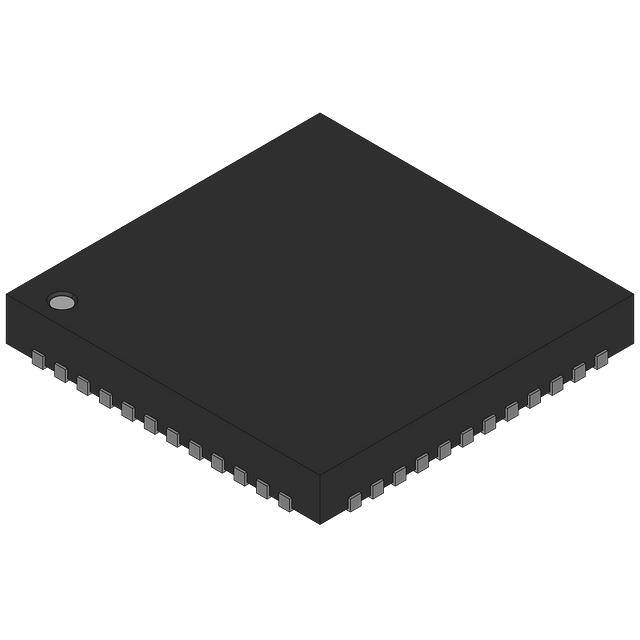


 工商网监
湘ICP备2023018690号
工商网监
湘ICP备2023018690号
