IS31FL3207
18-CHANNEL LED DRIVER WITH 16-BIT PWM
March 2020
GENERAL DESCRIPTION
FEATURES
The IS31FL3207 is an LED driver with 18 constant
current channels. Each channel can be pulse width
modulated (PWM) by 16 bits for smooth LED
brightness control. In addition, each channel has an
8-bit output current control register which allows fine
tuning the current for rich RGB color mixing, e.g., a
pure white color LED application. The maximum output
current of each channel can be adjusted by one 8-bit
global control register.
Proprietary programmable algorithms are used in
IS31FL3207 to minimize audible noise caused by the
MLCC decoupling capacitor. All registers can be
programmed via a high speed I2C (1MHz).
IS31FL3207 can be turned off with minimum current
consumption by either pulling the SDB pin low or by
using the software shutdown feature.
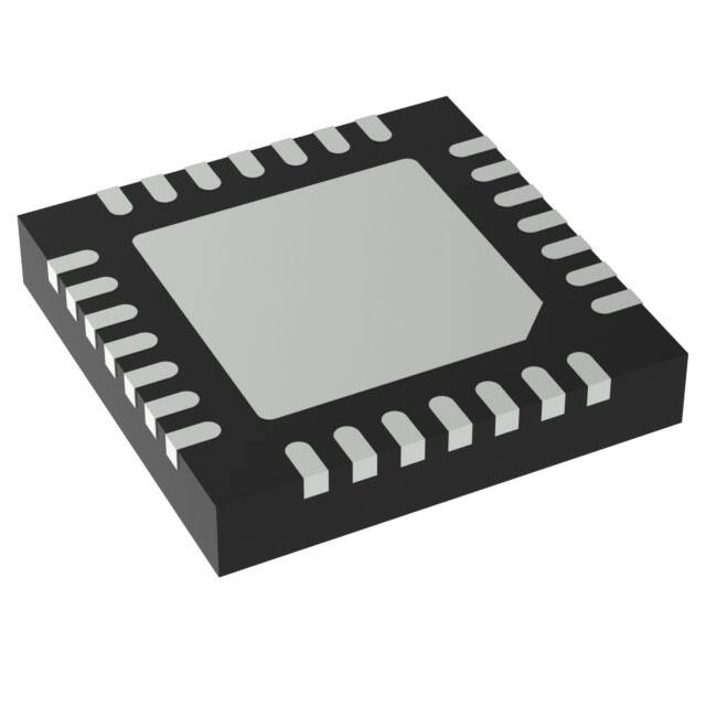
IS31FL3207 is available in QFN-28 (4mm × 4mm)
package. It operates from 2.7V to 5.5V over the
temperature range of -40°C to +125°C.
2.7V to 5.5V supply
Pin to pin with IS31FL3208A (QFN-28,
4mm×4mm)
Accuracy between channels and ICs: ≤ ±6%
1MHz I2C interface, automatic address increment
function with readout function
Four selectable I2C addresses
Accurate color rendition
- Selectable 8-bit/10-bit/12-bit/16-bit PWM
- 8-bit dot correction
- 8-bit global current adjust
Open/Short detect function
62kHz PWM frequency (8-bit PWM)
Temperature detect function
EMI reduction technology
- Spread spectrum
- Selectable Phase Delay
- Selectable 180 degree Clock Phase
-40°C to +125°C temperature range
QFN-28 (4mm × 4mm) package
APPLICATIONS
AI-speakers and smart home devices
Hand-held devices for LED display
LED in home appliances
TYPICAL APPLICATION CIRCUIT
Figure 1
Lumissil Microsystems – www.lumissil.com
Rev. A, 02/27/2020
Typical Application Circuit (VCC= Battery)
1
�IS31FL3207
TYPICAL APPLICATION CIRCUIT (CONTINUED)
*Note 1
*Note 4
VCC = 5V
3
8
VCC
33
*Note 1
VLED+ = 5V
OUT1
1 F
*Note 2
0.1 F
VIH
2k
9
91
10
33
26
33
27
91
28
33
OUT2
OUT3
2k
6
7
Micro
Controller
0.1 F 1
SDA
SCL
SDB
100k
IS31FL3207
OUT16
OUT17
*Note 3
5
RISET
3.3k
2
4,11
ISET
OUT18
AD
GND
GND
18,25
Figure 2 Typical Application Circuit (VCC= 5V)
Note 1: VLED+ should be same as VCC voltage.
Note 2: VIH is the high level voltage for IS31FL3207, which is usually same as VCC of Micro Controller, e.g. if VCC of Micro Controller is 3.3V,
VIH=3.3V. If VCC=5V and VIH is lower than 2.8V, recommend to add a level shift circuit for SDA and SCL.
Note 3: A 0.1µF capacitor is necessary for passing the EFT test.
2
Note 4: These optional resistors are for offloading the thermal dissipation (P=I R) away from the IS31FL3207.
Note 5: The maximum global output current is set up to 23mA when RISET= 3.3kΩ. The maximum global output current can be set by external
resistor, RISET. Please refer to the detail application information in RISET section.
Note 6: The IC and LED should be placed far away from the antenna in order to prevent the EMI.
Lumissil Microsystems – www.lumissil.com
Rev. A, 02/27/2020
2
�IS31FL3207
PIN CONFIGURATION
28 OUT18
27 OUT17
26 OUT16
25 GND
24 OUT15
23 OUT14
22 OUT13
OUT2 9
OUT3 10
GND 11
OUT4 12
OUT5 13
OUT6 14
Pin Configuration (Top View)
OUT1 8
Package
QFN-28
PIN DESCRIPTION
No.
Pin
Description
1
SDB
Shutdown the chip when pulled low.
2
AD
I2C address setting.
3
VCC
Power supply.
4,11,
18,25
GND
Ground.
5
ISET
Input terminal used to connect an external resistor. This
regulates the global output current.
6
SDA
I2C serial data.
7
SCL
I2C serial clock.
8~10
OUT1~OUT3
Output channel 1~3 for LEDs.
12~17
OUT4 ~ OUT9
Output channel 4~9 for LEDs.
19~24
OUT10 ~ OUT15
Output channel 10~15 for LEDs.
26~28
OUT16 ~ OUT18
Output channel 16~18 for LEDs.
Thermal Pad
Connect to GND.
Lumissil Microsystems – www.lumissil.com
Rev. A, 02/27/2020
3
�IS31FL3207
ORDERING INFORMATION
Industrial Range: -40°C to +125°C
Order Part No.
Package
QTY/Reel
IS31FL3207-QFLS4-TR
QFN-28, Lead-free
2500
Copyright © 2020 Lumissil Microsystems. All rights reserved. Lumissil Microsystems reserves the right to make changes to this specification and its
products at any time without notice. Lumissil Microsystems assumes no liability arising out of the application or use of any information, products or
services described herein. Customers are advised to obtain the latest version of this device specification before relying on any published information and
before placing orders for products.
Lumissil Microsystems does not recommend the use of any of its products in life support applications where the failure or malfunction of the product can
reasonably be expected to cause failure of the life support system or to significantly affect its safety or effectiveness. Products are not authorized for use in
such applications unless Lumissil Microsystems receives written assurance to its satisfaction, that:
a.) the risk of injury or damage has been minimized;
b.) the user assume all such risks; and
c.) potential liability of Lumissil Microsystems is adequately protected under the circumstances
Lumissil Microsystems – www.lumissil.com
Rev. A, 02/27/2020
4
�IS31FL3207
ABSOLUTE MAXIMUM RATINGS
Supply voltage, VCC
Voltage at SCL, SDA, SDB, AD, OUT1 to OUT18
Maximum junction temperature, TJMAX
Storage temperature range, TSTG
Operating temperature range, TA=TJ
Package thermal resistance, junction to ambient (4 layer standard
test PCB based on JESD 51-2A), θJA
ESD (HBM)
ESD (CDM)
-0.3V ~ +6.0V
-0.3V ~ VCC+0.3V
+150°C
-65°C ~ +150°C
-40°C ~ +125°C
51.3°C/W
±7kV
±750V
Note 7: Stresses beyond those listed under “Absolute Maximum Ratings” may cause permanent damage to the device. These are stress ratings
only and functional operation of the device at these or any other condition beyond those indicated in the operational sections of the specifications
is not implied. Exposure to absolute maximum rating conditions for extended periods may affect device reliability.
ELECTRICAL CHARACTERISTICS
Typical values are TA = 25°C, VCC = 5V.
Symbol
Parameter
Condition
VCC
Supply voltage
IMAX
Maximum global output current
VCC= 5V, VOUT= 0.8V, RISET= 2kΩ,
GCC= 0xFF, Scaling= 0xFF (Note 8)
IOUT
Output current
VCC= 5V, VOUT= 0.6V, RISET= 3.3kΩ,
GCC= 0xFF, SL= 0xFF
∆IMAT
VHR
ICC
ISD
Output current mismatch
between channels
Headroom voltage
Quiescent power supply current
Shutdown current
Min.
Typ. Max.
2.7
5.5
38
23
V
mA
24.61
mA
6
%
0.3
0.5
V
3.3
5
mA
2.7
4
mA
VCC= 5V, RISET= 3.3kΩ, VSDB= 0V or
software shutdown
2
3
μA
VCC= 3.6V, RISET= 3.3kΩ, VSDB= 0V or
software shutdown
1
2
μA
32
34
kHz
0.1
μA
RISET= 3.3kΩ, GCC= 0xFF,
VOUT= 0.6V, SL= 0xFF (Note 9)
GCC= 0xFF,RISET= 3.3kΩ,
IOUT= 20mA, SL= 0xFF
VCC= 5V, RISET= 3.3kΩ, GCC= 0xFF,
SL = 0xFF, IOUT= 23mA, PWM= 0x00
21.39
Unit
-6
VCC= 3.6V, RISET= 3.3kΩ, GCC= 0xFF,
SL = 0xFF, IOUT= 23mA, PWM= 0x00
fOUT
PWM frequency of output
PWM resolution 8-bit,
OSC clock 8MHz
IOZ
Output leakage current
VSDB= 0V or software shutdown,
VOUT= 5.5V
Thermal shutdown
(Note 10)
160
°C
(Note 10)
13
°C
TSHDN
TSHDNHYST Hysteresis
VISET
Output voltage of ISET pin
30
0.8
1.0
1.1
V
0.4
V
Logic Electrical Characteristics (SDA, SCL, SDB, AD)
VIL
Logic “0” input voltage
VCC= 2.7V~5.5V
VIH
Logic “1” input voltage
VCC= 2.7V~5.5V
IIL
Logic “0” input current
VINPUT= 0V (Note 10)
5
nA
IIH
Logic “1” input current
VINPUT= VCC (Note 10)
5
nA
Lumissil Microsystems – www.lumissil.com
Rev. A, 02/27/2020
1.4
V
5
�IS31FL3207
DIGITAL INPUT SWITCHING CHARACTERISTICS (NOTE 10)
Fast Mode
Symbol
Parameter
Min.
Typ. Max.
fSCL
Serial-clock frequency
tBUF
Fast Mode Plus
Min.
Typ.
Max.
Units
-
400
-
1000
kHz
Bus free time between a STOP and a START
condition
1.3
-
0.5
-
μs
tHD, STA
Hold time (repeated) START condition
0.6
-
0.26
-
μs
tSU, STA
Repeated START condition setup time
0.6
-
0.26
-
μs
tSU, STO
STOP condition setup time
0.6
-
0.26
-
μs
tHD, DAT
Data hold time (Note 11)
-
-
-
-
μs
tSU, DAT
Data setup time (Note 12)
100
-
50
-
ns
tLOW
SCL clock low period
1.3
-
0.5
-
μs
tHIGH
SCL clock high period
0.7
-
0.26
-
μs
tR
Rise time of both SDA and SCL signals,
receiving
-
300
-
120
ns
tF
Fall time of both SDA and SCL signals,
receiving
-
300
-
120
ns
Note 8: The recommended minimum value of RISET is 2kΩ, or it may cause a large current.
Note 9: ∆IMAT= (IOUT- IAVG)/IAVG×100%. IAVG= (IOUT1+IOUT2+…IOUT18)/18.
Note 10: Guaranteed by design.
Note 11: The minimum tHD, DAT measured start from VIL(max) of SCL signal. The maximum tHD,DAT has only to be met if the device does not stretch
the LOW period (tLOW) of the SCL signal. VIL(max).
Note 12: A Fast-mode I2C-bus device can be used in a Standard-mode I2C-bus system, but the requirement tSU,DAT≥ 250ns must then be met.
This will automatically be the case if the device does not stretch the LOW period of the SCL signal. If such a device does stretch the LOW period
of the SCL signal, it must output the next data bit to the SDA line tR max + tSU,DAT = 1000 + 250 = 1250ns (according to the Standard-mode
I2C-bus specification) before the SCL line is released.
Lumissil Microsystems – www.lumissil.com
Rev. A, 02/27/2020
6
�IS31FL3207
FUNCTIONAL BLOCK DIAGRAM
VCC
PWM
Control
SDA
SCL
Output
Driver
I2C
Interface
OUT1~OUT18
Register
Bias
AD
ISET
6 Group
CNT
Bandgap
MUX
SD_Chip
SDB
OSC
Spread
Spectrum
GND
Lumissil Microsystems – www.lumissil.com
Rev. A, 02/27/2020
7
�IS31FL3207
DETAILED DESCRIPTION
Then the master sends an SCL pulse. If the
IS31FL3207 has received the address correctly, then it
holds the SDA line low during the SCL pulse. If the
SDA line is not low, then the master should send a
“STOP” signal (discussed later) and abort the transfer.
I2C INTERFACE
The IS31FL3207 uses a serial bus, which conforms to
the I2C protocol, to control the chip’s functions with two
wires: SCL and SDA. The IS31FL3207 has a 7-bit
slave address (A7:A1), followed by the R/W bit, A0. Set
A0 to “0” for a write command and set A0 to “1” for a
read command. The value of bits A1 and A2 are
decided by the connection of the AD pin. The complete
slave address is:
Following acknowledge of IS31FL3207, the register
address byte is sent, most significant bit first.
IS31FL3207 must generate another acknowledge
indicating that the register address has been received.
Then 8-bit of data byte are sent next, most significant
bit first. Each data bit should be valid while the SCL
level is stable high. After the data byte is sent, the
IS31FL3207 must generate another acknowledge to
indicate that the data was received.
Table 1 Slave Address (Write Only):
Bit
A7:A3
A2:A1
Value
01101
AD
AD connected to GND, AD = 00;
AD connected to VCC, AD = 11;
AD connected to SCL, AD = 01;
AD connected to SDA, AD = 10;
A0
0
The “STOP” signal ends the transfer. To signal “STOP”,
the SDA signal goes high while the SCL signal is high.
ADDRESS AUTO INCREMENT
The SCL line is uni-directional. The SDA line is
bi-directional (open-drain) with a pull-up resistor
(typically 2kΩ). The maximum clock frequency
specified by the I2C standard is 1MHz. In this
discussion, the master is the microcontroller and the
slave is the IS31FL3207.
To write multiple bytes of data into IS31FL3207, load
the address of the data register that the first data byte
is intended for. During the IS31FL3207 acknowledge
of receiving the data byte, the internal address pointer
will increment by one. The next data byte sent to
IS31FL3207 will be placed in the new address, and so
on. The auto increment of the address will continue as
long as data continues to be written to IS31FL3207
(Figure 6).
The timing diagram for the I2C is shown in Figure 3.
The SDA is latched in on the stable high level of the
SCL. When there is no interface activity, the SDA line
should be held high.
READING OPERATION
The “START” signal is generated by lowering the SDA
signal while the SCL signal is high. The start signal will
alert all devices attached to the I2C bus to check the
incoming address against their own chip address.
Most of the registers can be read.
To read the register, after I2C start condition, the bus
master must send the IS31FL3207 device address
____
The 8-bit chip address is sent next, most significant bit
first. Each address bit must be stable while the SCL
level is high.
with the R/W bit set to “0”, followed by the register
address which determines which register is accessed.
Then restart I2C, the bus master should send the
After the last bit of the chip address is sent, the master
checks for the IS31FL3207’s acknowledge. The master
releases the SDA line high (through a pull-up resistor).
IS31FL3207 device address with the R/W bit set to
“1”. Data from the register defined by the command
byte is then sent from the IS31FL3207 to the master
(Figure 7).
Figure 3
Lumissil Microsystems – www.lumissil.com
Rev. A, 02/27/2020
____
Interface Timing
8
�IS31FL3207
Figure 4
Figure 5
Figure 6
Bit Transfer
Writing to IS31FL3207 (Typical)
Writing to IS31FL3207 (Automatic Address Increment)
Figure 7
Lumissil Microsystems – www.lumissil.com
Rev. A, 02/27/2020
Reading from IS31FL3207
9
�IS31FL3207
REGISTER DEFINITIONS
Table 2 Register Function
Address
Name
00h
Function
R/W
Table Default
Control Register
Power control register
R/W
3
PWM Register
Channel [18:1] PWM register byte
R/W
5
Update Register
Update the PWM and Scaling data
W
-
LED Scaling Register
Control each channel’s DC current
R/W
7
6Eh
Global Current Control Register
Control Global DC current/SSD
R/W
8
70h
Phase Delay and Clock Phase
Register
Phase Delay and Clock Phase
R/W
9
71h
Open Short Detect Enable Register
Open short detect enable
R/W
10
LED Open/Short Register
Open short information
R/W
11
77h
Temperature Sensor Register
Temperature information
R/W
12
78h
Spread Spectrum Register
Spread spectrum control register
R/W
13
7Fh
Reset Register
Reset all registers
W
-
01h~24h
49h
4Ah~5Bh
72h~74h
0000
0000
Table 4 PWM Frequency
Table 3 00h Control Register
PWM
16M
Resolution
Bit
D7
D6:D4
D3
D2:D1
D0
Name
-
OSC
-
PMS
SSD
8bit
62k 32k
4k
2k
1k
Default
0
000
0
00
0
10bit
16k
8k
1k
0.5k
244
122
NA
NA
12bit
4k
2k
244 122
NA
NA
NA
NA
NA
NA
NA
NA
NA
The Control Register sets software shutdown mode,
internal oscillator clock frequency and PWM
resolution. The internal oscillator clock frequency and
the PWM resolution will decide the output PWM
frequency. Recommend selecting PWM frequency
higher than 20kHz to avoid MLCC audible noise as
shown in Table 4.
SSD
0
1
Software Shutdown Enable
Software shutdown mode
Normal operation
PMS
00
01
10
11
PWM Resolution
N=256, 8-bit
N=1024, 10-bit
N=4096, 12-bit
N=65536, 16-bit
OSC
000
001
010
011
100
101
110
111
Oscillator Clock Frequency Selection
16MHz
8MHz
1MHz
500kHz
250kHz
125kHz
62kHz
31kHz
16bit
8M
244 122
1M 500k 250k 125k 62k 31k
NA
0.5k 244 122
Table 5 01h~24h PWM Register
Reg
02h (04h, 06h…)
01h (03h, 05h…)
Bit
D7:D0
D7:D0
Name
PWM_H
PWM_L
Default
0000 0000
0000 0000
Each output has 2 bytes to modulate the PWM duty
in 256/1024/4096/65536 steps. If using 8 bit PWM
resolution, only PWM_L bits need to be set.
The value of the SL (Scaling Register) decides the
peak current of each LED noted as IOUT.
IOUT and the value of the PWM Registers decide the
average current of each LED noted as ILED.
IOUT is computed by Formula (1):
I OUT I OUT ( MAX )
GCC
SL
256
256
(1)
ILED computed by Formula (2):
I LED
PWM
I OUT
N
N=256: PWM
(2)
7
D[ n ] 2
n
n0
Lumissil Microsystems – www.lumissil.com
Rev. A, 02/27/2020
10
�IS31FL3207
N=1024: PWM
Table 6 PWM and Scaling Register Map
PWM
OUT
SL
PWM_H
PWM_L
9
D[n ] 2
n
n0
N=4096: PWM
11
D[ n ] 2
n
n0
N=65536: PWM
15
D[ n ] 2
n
(3)
n0
Where IOUT(MAX) is the maximum output current
decided by RISET (Check RISET section for more
information), GCC is the global current setting (6Eh),
and SL is the scaling of each output (4Ah~6Dh),
N=256/1024/4096/65536(8/10/12/16
bit
PWM
resolution).
For example: RISET=3.3kΩ, GCC=0xFF, SL=0xFF,
PMS= “11” (16-bit PWM resolution), PWM_H=0xFF,
PWM_L=0xFF, IOUT(MAX)= 23.18mA.
I OUT I OUT ( MAX )
PWM
255 255
23 mA (1)
256 256
15
D[ n ] 2
n
65535
(3)
n0
N= 65536
I LED
65535
23 mA 23 mA
65536
(2)
Where IOUT(MAX) is the maximum output current
decided by RISET (Check RISET section for more
information).
The IOUT of each channel is set by the SL bits of LED
Scaling Register (4Ah~6Dh). Please refer to the detail
information in Table 7.
If RISET=3.3kΩ, GCC=0xFF, SL=0xFF, PMS= “00”
(8-bit PWM resolution, only use the PWM_L, the
PWM_H
will
be
ignored),
PWM_H=0x77,
PWM_L=0xAA, IOUT(MAX) = 23.18mA
I OUT I OUT ( MAX )
PWM
255 255
23 mA (1)
256 256
7
D[ n ] 2
n
170
(3)
n 0
N= 256
I LED
170
23 mA
256
1
2
3
4
5
6
7
8
9
10
11
12
13
14
15
16
17
18
02h
04h
06h
08h
0Ah
0Ch
0Eh
10h
12h
14h
16h
18h
1Ah
1Ch
1Eh
20h
22h
24h
Lumissil Microsystems – www.lumissil.com
Rev. A, 02/27/2020
4Ah
4Bh
4Ch
4Dh
4Eh
4Fh
50h
51h
52h
53h
54h
55h
56h
57h
58h
59h
5Ah
5Bh
49h Update Register
When SDB = “H” and SSD = “1”, a write of 00h to 49h
is to update the PWM Registers (01h~24h) values.
Table 7 4Ah~5Bh LED Scaling Register
Bit
D7:D0
Name
SL
Default
0000 0000
Each output has 8 bits to modulate DC current in 256
steps.
The value of the LED Scaling Registers decides the
DC peak current of each LED noted IOUT.
IOUT is computed by Formula (1):
I OUT I OUT ( MAX )
SL
(2)
01h
03h
05h
07h
09h
0Bh
0Dh
0Fh
11h
13h
15h
17h
19h
1Bh
1Dh
1Fh
21h
23h
GCC
SL
256
256
(1)
7
D[ n ] 2
n
(4)
n0
Where IOUT(MAX) is the maximum output current
decided by RISET, GCC is the global current setting
(6Eh).
4Ah~5Bh don’t need to update by 49h, each register
will be updated immediately when it is written.
11
�IS31FL3207
Table 8 6Eh Global Current Control Register
Bit
D7:D0
Name
GCC
Default
0000 0000
GCC and SL control the IOUT as shown in Formula (1).
GCC
7
D[ n ] 2
n
n0
(5)
If GCC=0xFF, SL=0xFF, IOUT=IOUT(MAX)
If GCC=0x01, SL=0xFF,
I OUT
1
255
I OUT ( MAX )
256 256
Where IOUT(MAX) is the maximum output current
decided by RISET (Check RISET section for more
information).
Table 9 70h Phase Delay and Clock Phase
Register
Bit
D7
D6:D3
D2
D1
D0
Name
PDE
-
PS3
PS2
PS1
Default
0
0000
0
0
0
IS31FL3207 features a 3 phase delay function, when
PDE bit is set, the phase delay function is enabled.
Phase Delay separates 18 outputs as 3 groups,
OUT1~OUT6 as group 1, OUT7~OUT12 as group 2,
OUT13~OUT18 as group 3. When Phase Delay is
enabled, group 2 has a 1/(3×fOUT) time delay than
group 1, group 3 also has a 1/(3×fOUT) time delay
than group 2.
Phase Delay feature and Clock Phase options can
work together to minimize the voltage ripple of LED
power supply.
PDE
0
1
Group Phase Delay Enable
Phase delay disable
Phase delay enable
PS1
0
1
OUT1~OUT6 Phase Select
Phase delay 0 Degree
Phase delay 180 Degree
PS2
0
1
OUT7~OUT12 Phase Select
Phase delay 0 Degree
Phase delay 180 Degree
PS3
0
1
OUT13~OUT18 Phase Select
Phase delay 0 Degree
Phase delay 180 Degree
Lumissil Microsystems – www.lumissil.com
Rev. A, 02/27/2020
Table 10 71h Open Short Detect Enable
Register
Bit
D7:D2
D1:D0
Name
-
OSDE
Default
0000 00
00
OSDE enables the open and/or short LED channel
detection with the result stored in 72h~76h, note
either open or short information is saved not both.
OSDE
00
01
10
11
Open Detect Enable
Detect disable
Detect disable
Short detect enable
Open detect enable
Table 11-1 72h LED Open/Short Register
Bit
D7:D0
Name
OP/ST[8:1]
Default
0000 0000
Table 11-2 73h LED Open/Short Register
Bit
D7:D0
Name
OP/ST[16:9]
Default
0000 0000
Table 11-3 74h LED Open/Short Register
Bit
D7:D2
D1:D0
Name
-
OP/ST[18:17]
Default
0000 00
00
Open or short status is stored in 72h to 74h.
OP[18:1]
0
1
Open Information of OUT18:OUT1
Open not detected
Open detected
ST[18:1]
0
1
Short Information of OUT18:OUT1
Short not detected
Short detected
Table 12 77h Temperature Sensor Register
Bit
D7:D6
D5
D4
D3:D2
D1:D0
Name
TROF
-
T_Flag
-
TS
Default
00
0
0
00
00
TS stores the temperature/thermal roll-off point.
TROF stores percentage of output current of the
thermal rool-off function.
Read T_Flag can indicate if the die temperature
exceeds the setting point (TS). Before each reading
of 77h register, TROF and TS need to be re-written.
12
�IS31FL3207
00
01
10
11
Thermal roll off percentage of output
current
100%
75%
55%
30%
T_Flag
0
1
Temperature Flag
Temperature point not exceeded
Temperature point exceeded
TS
Temperature Point, Thermal roll off
start point
140°C
120°C
100°C
90°C
TROF
00
01
10
11
Table 13 78h Spread Spectrum Register
Bit
D7:D5
D4
D3:D2
D1:D0
Name
DCPWM
SSP
RNG
CLT
Default
000
0
00
00
SSP
0
1
Spread Spectrum Enable
Disable
Enable
RNG
00
01
10
11
Spread Spectrum Range
±5%
±15%
±24%
±34%
CLT
00
01
10
11
Spread Spectrum Cycle Time
1980μs
1200μs
820μs
660μs
7Fh Reset Register
When SDB = “H” and SSD = “1”, a write of “0000
0000” to 7Fh will reset all registers to their default
values.
When DCPWM is set to “0”, the PWM outputs are
decided by 01h~48h, and the PWM range is
0/256~255/256(8-bit PWM, 0/1024~1023/1024 for 10
bit PWM, 0/4096~4095/4096 for 12 bit PWM,
0/65536~65535/65536 for 16 bit PWM), still the
1/256(8-bit PWM, 1/1024 for 10 bit PWM, 1/4096 for
12 bit PWM, 1/65536 for 16 bit PWM), can’t be
turned on. When the DCPWM is set to “1”, PWM
dimming is disabled and dimming will be done by
current adjust GCC and SL registers.
Spread spectrum register configures the spread
spectrum function, adjust the cycle time and range.
DCPWM
xx0
xx1
x0x
x1x
Setting the output to work in DC mode
Output 1~12 PWM data set by
registers 01h~18h
Output 1~12 set to turn on (PWM is
disabled)
Output 13~18 PWM data set by
registers 19h~24h
Output 13~18 set to turn on (PWM is
disabled)
Lumissil Microsystems – www.lumissil.com
Rev. A, 02/27/2020
13
�IS31FL3207
APPLICATION INFORMATION
RISET
The maximum output current IOUT(MAX) of
OUT1~OUT18 can be adjusted by the external
resistor, RISET, as described in Formula (6).
I OUT ( MAX ) x
V ISET
R ISET
(6)
x = 76.5, VISET = 1.0V.
The recommended minimum value of RISET is 2kΩ.
When RISET=3.3kΩ, IOUT(MAX)=23.18mA
When RISET=2kΩ, IOUT(MAX)=38.25mA
RISET should be close to the chip and the ground side
should well connect to the GND plane.
CURRENT SETTING
The maximum output current is set by the external
register RISET. The current of each output can also be
set independently by the SL 8 bits of LED Scaling
Register (4Ah~5Bh).
Some applications may require the IOUT of each
channel need to be adjusted independently. For
example, if OUT1 drives 1 LED and OUT2 drives 2
parallel LEDs, and they should have the same
average current like 18mA, we can set the IOUT(MAX) to
36mA, and GCC=0xFF, 4Ah=0x80, 4Bh=0xFF, the
OUT1 sinks about 18mA and OUT2 sinks 36mA
which can have two LEDs in parallel.
Another example, OUT1, OUT2 and OUT3 drive an
RGB LED, OUT1 is Red LED, OUT2 is Green LED
and OUT 3 is Blue LED, with same RISET, GCC and
same SL bits, when OUT1 OUT2 and OUT3 have the
same PWM value, the LED may looks a litter pink, or
not so white, in this case, the SL bits can be used to
adjust the single IOUTx of some output and make it
pure white color. We call this SL bits another name:
white balance registers.
PWM CONTROL
The PWM Registers (01h~24h) can modulate LED
brightness
of
each
18
channels
with
256/1024/4096/65536 steps. For example, if the data
in PWM_H Register is “0000 0000” and in PWM_L
Register is “0000 0100”, then the PWM is the fourth
step.
Writing new data continuously to the registers can
modulate the brightness of the LEDs to achieve a
breathing effect.
PWM FREQUENCY SELECT
The IS31FL3207 output channels operate with a
default 8 bit PWM resolution and the PWM frequency
of 62kHz (the oscillator frequency is 16MHz).
Lumissil Microsystems – www.lumissil.com
Rev. A, 02/27/2020
Because all the OUTx channels are synchronized,
the DC power supply will experience large
instantaneous current surges when the OUTx
channels turn ON. These current surges will generate
an AC ripple on the power supply which cause stress
to the decoupling capacitors. When the AC ripple is
applied to a monolithic ceramic capacitor chip (MLCC)
it will expand and contract causing the PCB to flex
and generate audible hum in the range of between
300Hz to 18kHz, To avoid this hum, there are many
countermeasures, such as selecting the capacitor
type and value which will not cause the PCB to flex
and contract.
An additional option for avoiding audible hum is to set
the
IS31FL3207’s
output
PWM
frequency
above/below the audible range. The Contorl Register
(00h) can be used to set the switching frequency to
122Hz~62kHz as shown in Table 4, some combine
setting of the OSC and PMS bits will get different
output PWM frequency, and higher than 20kHz is out
of the audible range.
OPEN/SHORT DETECT FUNCTION
IS31FL3207 has open and short detect bit for each
LED.
By setting the OSDE bit of Open Short Detect Enable
Register (71h) from “00” to “10” (store short
information) or “11” (store open information), the LED
Open/Short Register will store the open/short
information immediately the MCU can get the
open/short information by reading the 72h~74h.
SPREAD SPECTRUM FUNCTION
PWM current switching of LED outputs can be
particularly troublesome when the EMI is concerned.
To optimize the EMI performance, the IS31FL3207
includes a spread spectrum function. By setting the
RNG bit of Spread Spectrum Register (78h), Spread
Spectrum range can be choose from ±5% /±15%
/±24% /±34%. The spread spectrum function will
lower the total electromagnetic emitting energy by
spreading the energy into a wider range to
significantly degrade the peak energy of EMI. With
spread spectrum, the EMI test is easier to pass with a
smaller size and lower cost filter circuit.
OPERATING MODE
IS31FL3207 can only operate in PWM Mode. The
brightness of each LED can be modulated with
256/1024/4096/65536 steps by PWM registers. For
example, if the data in PWM Register is “0000 0100”,
then the PWM is the fourth step.
Writing new data continuously to the registers can
modulate the brightness of the LEDs to achieve a
breathing effect.
14
�IS31FL3207
SHUTDOWN MODE
Shutdown mode can be used as a means of reducing
power consumption. During shutdown mode all
registers retain their data.
Software Shutdown
By setting the SSD bit of the Control Register (00h) to
“0”, the IS31FL3207 will operate in software
shutdown mode. When the IS31FL3207 is in software
shutdown, all current sources are switched off, so the
LEDs are OFF but all registers accessible. Typical
current consume is 1μA (VCC=3.6V).
Hardware Shutdown
The chip enters hardware shutdown when the SDB
pin is pulled low. All analog circuits are disabled
during hardware shutdown, typical the current
consumption is 1μA (VCC=3.6V).
The chip releases hardware shutdown when the SDB
pin is pulled high. The rising edge of SDB pin will
reset the I2C module, but the register information
retains. During hardware shutdown the registers are
accessible.
If the VCC supply drops below 1.75V but remains
above 0.1V during SDB pulled low, please re-initialize
all Function Registers before SDB pulled high.
LAYOUT
The IS31FL3207 consumes lots of power so good
PCB layout will help improve the reliability of the chip.
Please consider below factors when layout the PCB.
also the digital and analog blocks’ supply line and
GND should be separated to avoid the noise from
digital block affect the analog block.
At least one 0.1μF capacitor, if possible with a 1μF
capacitor is recommended to connected to the
ground at power supply pin of the chip, and it needs
to close to the chip and the ground net of the
capacitor should be well connected to the GND
plane.
RISET
RISET should be close to the chip and the ground side
should well connect to the GND plane.
Thermal Consideration
The over temperature of the chip may result in
deterioration of the properties of the chip. The thermal
pad of IS31FL3207 should connect to GND net and
need to use 4 or 9 vias connect to GND copper area,
the GND area should be as large area as possible to
help radiate the heat from the IS31FL3207.
Current Rating Example
For a RISET=3.3kΩ application, the current rating for
each net is as follows:
• VCC pin maximum current is 5mA when VCC=5V,
but the VLED+ net is provide total current of all
outputs,
its
current
can
as
much
as
23mA×18=414mA,
recommend trace width for
VCC pin: 0.20mm~0.3mm, recommend trace width
for VLED+ net: 0.25mm~0.5mm,
Power Supply Lines
• Output pins=23mA, recommend trace width is
0.2mm~0.254mm
When designing the PCB layout pattern, the first step
should consider about the supply line and GND
connection, especially those traces with high current,
• All other pins


 工商网监
湘ICP备2023018690号
工商网监
湘ICP备2023018690号
