IS31FL3195
CHARGE PUMP RGBW LED DRIVER
WITH PROGRAMMABLE SELF-RUNNING PATTERNS
May 2019
GENERAL DESCRIPTION
The IS31FL3195 is a compact and efficient 4-channel
charge pump LED driver with programmable sequence
operation for automated RGBW lighting effects. It is
capable of driving 1 to 4 LEDs with a low drop-out and
current matching so all 4 LEDs maintain consistent
brightness. Each channel can support up to 20mA of
current.
The built−in charge pump (CP) structure will
automatically toggle between 1x, 1.5x operation
depending on the battery’s state of charge. This
DC/DC converter operates at a high switching
frequency which enables the use of small external
capacitors and achieves 92% peak total efficiency. The
IS31FL3195 is optimized for battery applications. To
conserve battery life, the charge pump goes into high
impedance mode whenever the IS31FL3195 is
shutdown consuming less than 1µA.
The IS31FL3195 can operate in either “Current Level”
or “Programmable Sequence” mode. In Current Level
mode, the average output current of each output is
independently programmed and controlled in 256
PWM steps to simplify color mixing. In programmable
sequence mode, the timing characteristics for each
output can be individually adjusted to maintain a
pre-established pattern sequence without requiring
any additional MCU interaction, thus saving valuable
system resources.
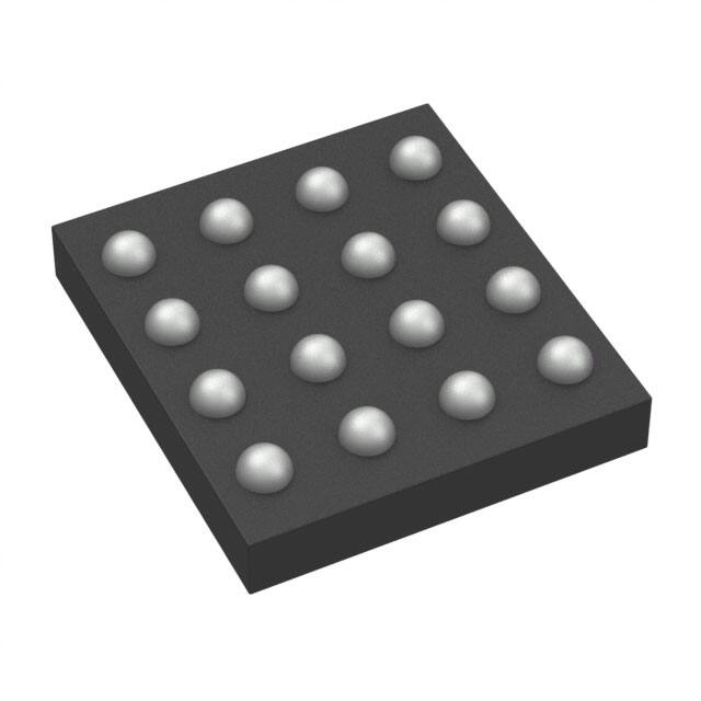
The IS31FL3195 is available in a small QFN-16 (4mm
× 4mm) and WLCSP-16 (1.88mm×2.08mm, 0.45mm
ball pitch, 0.2mm ball diameter) packages. It operates
from 2.7V to 5.5V over the temperature range of -40°C
to +85°C.
With automated lighting effects and a DC/DC charge
pump, the small package IS31FL3195 is ideal for low
power battery applications.
FEATURES
APPLICATIONS
Lumissil Microsystems – www.lumissil.com
Rev. A, 04/18/2019
2.7V to 5.5V supply voltage
Charge pump
- 1x, 1.5x operating modes
- Highly efficient across battery state of charge
- 1MHz constant frequency
- Enter 1.5x mode if any of the four OUTx pins <
150mV (50mV~300mV selectable)
Power saving operating
- 1µA Shutdown current
- 640µA Quiescent operating current (CP1x
mode)-Two selectable sleep modes
- Sleep 1 Mode: 38µA
- Sleep 2 Mode: 1µA
- Auto sleep mode if all OUTx outputs are off for
>30s.
Support four LEDs - RGBW
- Resistor sets LED current up to 20mA
- 8-bit dot correction
LEDs can operate with pre-established lighting
patterns
- Run without a micro
- Fixed number of iterations or non-stop operation
- Each channel has its own fade registers (TS-T4)
with independent start/stop
1MHz I2C bus interface
- Automatic address increment function
- 4 selectable I2C address locations
Over-temperature protection
QFN-16
(4mm×4mm)
and
WLCSP-16
(1.88mm×2.08mm, 0.45mm ball pitch, 0.2mm ball
diameter) packages
Operating temperature range is -40°C ~ +85°C
Internet-of-Things (IOT)
Low-power battery applications
Wearable applications
Hand-held devices requiring visual notifications
1
�IS31FL3195
TYPICAL APPLICATION CIRCUIT
3.3V~5.5V
VCC
1 F
C1P
C1N
0.1 F
C2P
3.3V
3.3V
4.7k
1 F
1 F
C2N
4.7k
VOUT
SDA
Micro
Controller
SCL
1 F
IS31FL3195
SDB
OUT1
100k
OUT2
ISET
IGMAX=20mA
RISET
AD
12k
GND
Figure 1
Lumissil Microsystems – www.lumissil.com
Rev. A, 04/18/2019
OUT3
OUT4
Typical Application Circuit
2
�IS31FL3195
PIN CONFIGURATION
Package
Pin Configuration (Top View)
QFN-16
WLCSP-16
ISET
SDA
OUT1
OUT2
A1
A2
A3
A4
GND
SDB
SCL
OUT3
B1
B2
B3
B4
C2P
C2N
AD
OUT4
C1
C2
C3
C4
C1P
C1N
VCC
VOUT
D1
D2
D3
D4
Lumissil Microsystems – www.lumissil.com
Rev. A, 04/18/2019
3
�IS31FL3195
PIN DESCRIPTION
No.
Pin
Description
1~4
A3, A4,
B4, C4
OUT1~OUT4
LED current sink pins, connect the corresponding LED
cathode to this pin. The anode of the associated LED must to
be connected to the VOUT pin. The unused channel can be
float but need to shut down by 01h register.
5
D4
VOUT
Charge pump output supplies the LED current. In shutdown
mode this pin is high impedance. Connect a 1μF capacitor
from VOUT to GND.
6
D3
VCC
Power supply input, requires 1.0μF and 0.1μF capacitor
between this pin and ground pin.
7,8
D1, D2
C1P,C1N
Stage 1 charge pump flying capacitor, C1N negative
terminal, C1P positive terminal. (Note 1)
9,10
C2, C1
C2N,C2P
Stage 2 charge pump flying capacitor, C2N negative
terminal, C2P positive terminal. (Note 1)
11
B1
GND
Ground reference signal for the charge pump and the output
current control. A PCB ground plane strongly recommended.
12
A1
ISET
Connect external resistor RISET to ground to set global max
current IGMAX.
13
B2
SDB
Pull below 0.4V to activate low power shutdown mode.
14
C3
AD
I2C address setting.
15
A2
SDA
I2C data pin. The SDA byte is used to program the device
operating mode.
16
B3
SCL
I2C serial clock associated with SDA signal.
Thermal Pad
Connect to GND.
QFN
WLCSP
Note 1: The flying capacitors should be placed as close as possible to the IC and the signal trace between the capacitor and CP terminals kept
as short as possible.
Lumissil Microsystems – www.lumissil.com
Rev. A, 04/18/2019
4
�IS31FL3195
ORDERING INFORMATION
Industrial Range: -40°C to +85°C
Order Part No.
Package
QTY/Reel
IS31FL3195-QFLS2-TR
IS31FL3195-CLS2-TR
QFN-16, Lead-free
WLCSP-16, Lead-free
2500
3000
Copyright © 2019 Lumissil Microsystems. All rights reserved. Lumissil Microsystems reserves the right to make changes to this specification and its
products at any time without notice. Lumissil Microsystems assumes no liability arising out of the application or use of any information, products or
services described herein. Customers are advised to obtain the latest version of this device specification before relying on any published information and
before placing orders for products.
Lumissil Microsystems does not recommend the use of any of its products in life support applications where the failure or malfunction of the product can
reasonably be expected to cause failure of the life support system or to significantly affect its safety or effectiveness. Products are not authorized for use
in such applications unless Lumissil Microsystems receives written assurance to its satisfaction, that:
a.) the risk of injury or damage has been minimized;
b.) the user assume all such risks; and
c.) potential liability of Lumissil Microsystems is adequately protected under the circumstances
Lumissil Microsystems – www.lumissil.com
Rev. A, 04/18/2019
5
�IS31FL3195
ABSOLUTE MAXIMUM RATINGS
Supply voltage, VCC, VOUT
Voltage at any input pin
Maximum junction temperature, TJMAX
Operating temperature range, TA=TJ
Storage temperature range, TSTG
Package thermal resistance, junction to ambient (4 layer
standard test PCB based on JESD 51-2A standard), θJA
ESD (HBM)
ESD (CDM)
-0.3V ~ +6.0V
-0.3V ~ VCC+0.3V
+150°C
-40°C ~ +85°C
-65°C ~ +150°C
53.8°C/W (QFN)
71.41°C/W (WLCSP)
±8kV
±750V
Note 2: Stresses beyond those listed under “Absolute Maximum Ratings” may cause permanent damage to the device. These are stress
ratings only and functional operation of the device at these or any other condition beyond those indicated in the operational sections of the
specifications is not implied. Exposure to absolute maximum rating conditions for extended periods may affect device reliability.
ELECTRICAL CHARACTERISTICS
TA= -40°C ~ +85°C, VCC= 3.6V, unless otherwise noted. Typical value are TA= 25°C.
Symbol
VCC
ICC
Parameter
Condition
Supply voltage
Quiescent operating
current
Min. Typ. Max. Unit
2.7
5.5
V
1x mode, all outputs disable
640
µA
1.5x mode, all outputs disable
1.2
mA
Sleep 1 Mode: CP stops, Bandgap working
and all OUTx are off without any bias
38
µA
Sleep 2 Mode: CP, Bandgap stop and all OUTx
are off without any bias
1
µA
VSDB= 0V
1
µA
VSDB= VCC, software shutdown
1
µA
ISD
Shutdown current
IOUT
Total output current
Current Level Mode, CL Register= 0xFF
Current set Register 20mA
80
mA
ILED
Current per channel
Current Level Mode, CL Register= 0xFF
Current set Register 20mA, VOUT=0.3V
20
mA
IMAT
Current matching
IACC
Current accuracy
VHR
Current sink headroom
voltage
ET
Total operating efficiency
VOVP
Any two outputs, VCC= 3.6V, IOUT= 20mA
VOUT=0.3V
-5
5
%
Any two outputs, VCC= 3.6V, IOUT= 5mA
VOUT=0.3V
-6
6
%
Any outputs, VCC= 3.6V, IOUT= 20mA
-8
8
%
Any outputs, VCC= 3.6V, IOUT= 5mA
-10
10
%
IOUT= 15mA
150
mV
VCC= 3.4V, VF= 3.2V, ILOAD= 20mA×4 channel
92
%
VCC= 2.7V, VF= 3.2V, ILOAD= 20mA×4 channel
77
%
Output voltage compliance
Output voltage clamp
(OVP)
4.4
5.5
V
Charge Pump Characteristics
tST
Soft-start time
fCLK
Charge pump operating
frequency
DC/DC start time (COUT= 1µF)
3.0V< VCC< 5.5V
64
µs
900 1000 1200 kHz
Lumissil Microsystems – www.lumissil.com
Rev. A, 04/18/2019
6
�IS31FL3195
ELECTRICAL CHARACTERISTICS(CONTINUED)
TA= -40°C ~ +85°C, VCC= 3.6V, unless otherwise noted. Typical value are TA= 25°C.
Symbol
Parameter
Condition
Min. Typ. Max. Unit
Logic Electrical Characteristics (SDA, SCL, AD, SDB)
VIL
Logic “0” input voltage
VCC = 2.7V~5.5V
0
0.4
V
VIH
Logic “1” input voltage
VCC = 2.7V~5.5V
1.4
VCC
V
IIL
Logic “0” input current
VINPUT = 0V (Note 3)
5
nA
IIH
Logic “1” input current
VINPUT = VIO (Note 3)
5
nA
DIGITAL INPUT SWITCHING CHARACTERISTICS (NOTE 3)
Symbol
Parameter
Fast Mode
Min.
Typ.
Fast Mode Plus
Typ.
Max.
Units
Max.
Min.
-
400
-
1000
kHz
fSCL
Serial-clock frequency
tBUF
Bus free time between a STOP and a START
condition
1.3
-
0.5
-
μs
tHD, STA
Hold time (repeated) START condition
0.6
-
0.26
-
μs
tSU, STA
Repeated START condition setup time
0.6
-
0.26
-
μs
tSU, STO
STOP condition setup time
0.6
-
0.26
-
μs
tHD, DAT
Data hold time
-
-
-
-
μs
tSU, DAT
Data setup time
100
-
50
-
ns
tLOW
SCL clock low period
1.3
-
0.5
-
μs
tHIGH
SCL clock high period
0.7
-
0.26
-
μs
tR
Rise time of both SDA and SCL signals,
receiving
-
300
-
120
ns
tF
Fall time of both SDA and SCL signals,
receiving
-
300
-
120
ns
Note 3: Guaranteed by design.
Lumissil Microsystems – www.lumissil.com
Rev. A, 04/18/2019
7
�IS31FL3195
FUNCTION BLOCK DIAGRAM
Lumissil Microsystems – www.lumissil.com
Rev. A, 04/18/2019
8
�IS31FL3195
DETAILED DESCRIPTION
I2C INTERFACE
The IS31FL3195 uses a serial bus, which conforms
to the I2C protocol, to control the chip’s functions with
two wires: SCL and SDA. The IS31FL3195 has a
constant 7-bit slave address (A7:A1), followed by the
R/W bit, A0. Set A0 to “0” for a write command and
set A0 to “1” for a read command. The value of bits
A1 and A2 are decided by the connection of the AD
pin.
The complete slave address is:
Table 1 Slave Address:
AD
A7:A3
A2:A1
GND
00
SCL
01
SDA
10101
VCC
10
A0
0/1
11
AD connected to GND, A2:A1=00;
AD connected to VCC, A2:A1=11;
AD connected to SCL, A2:A1=01;
AD connected to SDA, A2:A1=10;
Following acknowledge of IS31FL3195, the register
address byte is sent, most significant bit first.
IS31FL3195 must generate another acknowledge
indicating that the register address has been
received.
Then 8-bit of data byte are sent next, most significant
bit first. Each data bit should be valid while the SCL
level is stable high. After the data byte is sent, the
IS31FL3195 must generate another acknowledge to
indicate that the data was received.
The “STOP” signal ends the transfer. To signal
“STOP”, the SDA signal goes high while the SCL
signal is high.
The SCL line is uni-directional. The SDA line is
bi-directional (open-collector) with a pull-up resistor
(typically 4.7kΩ when SCL frequency is 400kHz).
The maximum clock frequency specified by the I2C
standard is 400kHz. In this discussion, the master is
the microcontroller and the slave is the IS31FL3195.
The timing diagram for the I2C is shown in Figure 2.
The SDA is latched in on the stable high level of the
SCL. When there is no interface activity, the SDA line
should be held high.
The “START” signal is generated by lowering the
SDA signal while the SCL signal is high. The start
signal will alert all devices attached to the I2C bus to
check the incoming address against their own chip
address.
The 8-bit chip address is sent next, most significant
bit first. Each address bit must be stable while the
SCL level is high.
Figure 2
Lumissil Microsystems – www.lumissil.com
Rev. A, 04/18/2019
After the last bit of the chip address is sent, the
master checks for the IS31FL3195’s acknowledge.
The master releases the SDA line high (through a
pull-up resistor). Then the master sends an SCL
pulse. If the IS31FL3195 has received the address
correctly, then it holds the SDA line low during the
SCL pulse. If the SDA line is not low, then the master
should send a “STOP” signal (discussed later) and
abort the transfer.
ADDRESS AUTO INCREMENT
To write multiple bytes of data into IS31FL3195, load
the address of the data register that the first data byte
is intended for. During the IS31FL3195 acknowledge
of receiving the data byte, the internal address
pointer will increment by one. The next data byte sent
to IS31FL3195 will be placed in the new address,
and so on (Figure 5).
READING PORT REGISTERS
To read the device data, the bus master must first
send the IS31FL3195 address with the R/W bit set to
“0”, followed by the command byte, which determines
which register is accessed. After a restart, the bus
master must then send the IS31FL3195 address with
the R/W bit set to “1”. Data from the register defined
by the command byte is then sent from the
IS31FL3195 to the master (Figure 6).
Interface Timing
9
�IS31FL3195
Figure 3
Figure 4
Figure 5
Bit Transfer
Writing to IS31FL3195 (Typical)
Writing to IS31FL3195 (Automatic Address Increment)
Figure 6
Reading from IS31FL3195
Lumissil Microsystems – www.lumissil.com
Rev. A, 04/18/2019
10
�IS31FL3195
Table 2 Registers Definitions
Address
Name
Function
R/W Table
Default
00h
Product ID
For read only, read result is
Slave address
R
-
-
01h
Shutdown Control Register
Set power down mode and
outputs shutdown control
W
3
1111 0000
02h
Operation Mode Configure
Register
Set output operation mode
W
4
0000 0000
03h
Charge Pump Setting-1
Set change pump
parameters
W
5
0010 0000
04h
Charge Pump Setting-2
Set change pump
parameters
W
6
0011 0000
05h
Current Band Register
Set current band of each
Output
W
7
0101 0101
06h
Hold Function Register
Set the hold function of each
Output
W
8
0000 0000
07h
Phase Delay Register
Phase delay mode setting
W
9
0000 0001
For reading the pattern
running state
R
10
0000 0000
Output current level data
register
W
11
0000 0000
10h~12h/20h~22h/ Color 1 Setting Register of
30h~32h/40h~42h P1/P2/P3/P4
Output current level data
register-Color 1
W
12~15 0000 0000
13h~15h/23h~25h/ Color 2 Setting Register of
33h~35h/43h~45h P1/P2/P3/P4
Output current level data
register-Color 2
W
12~15 0000 0000
16h~18h/26h~28h/ Color 3 Setting Register of
36h~38h/46h~48h P1/P2/P3/P4
Output current level data
register-Color 3
W
12~15 0000 0000
0Ch/0Dh/0Eh/0Fh P1/P2/P3/P4 State Register
10h/21h/32h/40h
OUT1/OUT2/OUT3/OUT4 Current
Level Register
19h/29h/39h/49h
P1/P2/P3/P4 TS &T1 Setting
Register
Set the TS~T1 time
W
16
0000 0000
1Ah/2Ah/3Ah/4Ah
P1/P2/P3/P4 T2 &T3 Setting
Register
Set the T2~T3 time
W
17
0000 0000
1Bh/2Bh/3Bh/4Bh
P1/P2/P3/P4 TP &T4 Setting
Register
Set the TP~T4 time
W
18
0000 0000
1Ch/2Ch/3Ch/4Ch
P1/P2/P3/P4 Color Enable
Register
Set the color enable/disable
W
19
0000 0001
1Dh/2Dh/3Dh/4Dh
P1/P2/P3/P4 Color Cycle Times
Register
Set color repeat time
W
20
0000 0000
Set next step and Gamma of
each pattern
W
1Eh/2Eh/3Eh/4Eh P1/P2/P3/P4 NXT Register
1Fh/2Fh/3Fh/4Fh P1/P2/P3/P4 Loop Times Register Set the loop time of P1~P4
50h
51h/52h/53h/54h
5Fh
21~24 0000 0001
W
25
0000 0000
Color Update Register
Update color data
W
-
0000 0000
P1/P2/P3/P4 Update Register
Update the time data and
start to run pattern
W
-
0000 0000
Reset Register
Reset the registers value to
default
W
-
0000 0000
Note: When T1 or T3= 0.03s, GAM will be set to 10 (Linearity).
Lumissil Microsystems – www.lumissil.com
Rev. A, 04/18/2019
11
�IS31FL3195
Table 3 01h Shutdown Control Register
Bit
D7:D4
D3
D2:D1
D0
Name
EN4:EN1
CPPM
SLE
SSD
Default
1111
0
00
0
The Shutdown Control Register sets software
shutdown and sleep modes of IS31FL3195.
The Output Enable Register enables/disables the
outputs independently. The ENx is only effective
when SSD= “1”.
Sleep 1 (power saving standby 1) Mode: CP in 1x
mode and all OUTx are off without any bias.
I_SLEEP1=35µA (Typ.)
Sleep 2 (power saving standby 2) Mode: CP off and
all OUTx are off without any bias. I_SLEEP2=1µA
(Typ.)
When SLE bits are set to “01” or “10”, IS31FL3195
puts itself in Sleep 1 or Sleep 2 Modes if all OUTx
outputs are off for >30s. MCU command to the
IS31FL3195 will wake it up and disable the sleep
mode.
The CPPM bit selects the default charge pump
power up mode. When CPPM= “0”, the default power
up mode is 1x mode, otherwise it will run in 1.5x
mode to ensure the LEDs can work with enough
forward voltage.
SSD
0
1
Software Shutdown Enable
Software shutdown mode
Normal operation
SLE
00/11
01
10
Sleep Mode Enable
Sleep mode disable
Sleep1 mode enable
Sleep2 mode enable
When LM= “00/11”, the OUTx can be “0” current level
mode or “1” pattern mode, when LM= “01”, the OUT4
can be “0” current level mode or “1” pattern mode,
OUT1~3 are not needed to set. When LM= “10”,
OUT1~4 are not needed to set.
LM
00/11
01
10
OUTx
0
1
LED Mode
Single mode
RGB + W mode, OUT1, OUT2 and OUT3
work together, OUT4 work independent
RGBY mode, OUT1, OUT2, OUT3 and
OUT4 work together thru Pattern 1-3
Output Operating Mode
Current Level Mode
Pattern Mode
Table 5 03h Charge Pump Setting-1
Bit
D7:D2
D1:D0
Name
-
CPM
Default
0010 00
00
The Charge Pump Setting Register-1 sets the charge
pump working mode.
CPM
00
01
10
Charge Pump Working Mode
Auto mode
1x mode
1.5x mode
Table 6 04h Charge Pump Setting-2
CPPM
0
1
Charge Pump Power Up Mode
1x
1.5x
ENx
0
1
Output Enable Control
Output disable
Output enable
Bit
D7
D6:D4
D3:D0
Name
-
HRT
CPDE4:CPDE1
Default
0
011
0000
The Charge Pump Setting Register-2 sets headroom
detect threshold voltage and enables OUTx charge
pump detection. Disable charge pump detection on
OUTx if LED anode not connected to VOUT or OUTx
floating.
CPDEx
Table 4 02h Operating Configure Register
Bit
D7:D4
D3:D1
D1:D0
Name
OUT4:OUT1
-
LM
Default
0000
00
00
0
1
Charge Pump Detection Enable of
OUTx
Enable
Disable
The Operating Configure Register sets operation
modes of IS31FL3195.
Lumissil Microsystems – www.lumissil.com
Rev. A, 04/18/2019
12
�IS31FL3195
HRT
000
001
010
011
100
101
110
111
Table 9 07h Phase Delay Register
Headroom Threshold Voltage
50mV
100mV
125mV
150mV
175mV
200mV
250mV
300mV
D7:D6
D5:D4
D3:D2
D1:D0
Name
CB4
CB3
CB2
CB1
Default
01
01
01
01
Current Band Setting
Band 1: 0mA~IGMAX ×1/4, IBAND= IGMAX × 1/4
Band 2: 0mA~ IGMAX ×1/2, IBAND= IGMAX × 1/2
Band 3: 0mA~ IGMAX ×3/4, IBAND= IGMAX × 3/4
Band 4: 0mA~ IGMAX, IBAND= IGMAX
Table 8 06h Hold Function Register
D6
D5
D4
D3
D2
D1
D0
Name HF4 HT4 HF3 HT3 HF2 HT2 HF1 HT1
Default
0
0
0
0
0
0
0
1
HFx
0
1
Hold Time Selection
Hold at end of T4 when pattern loop done
(always off)
Hold at end of T2 when pattern loop done
(always on)
Hold Function Enable
Hold function disable
Hold function enable
-
PD
Default
0000 00
01
Phase Delay Mode
Phase delay mode 1
Phase delay mode 2
Bit
D7
Name
PSx
Default
0
D6
D5
D4
CS3x CS2x CS1x
0
0
0
D3
D2:D0
-
TXx
0
000
The Pattern State Registers store the four patterns.
PS is the pattern enable or not, CSX is the color
enable or not, TX will show the running position of
Pattern 1.
ODh, OEh and 0Fh store the state of Pattern 2, 3 and
4.
TXx
000
001
010
011
100
101
Time State
Running at TS
Running at T1
Running at T2
Running at T3
Running at TP
Running at T4
CSXx
0
1
Color State
Not running at Color x
Running at Color x
PSx
0
1
Pattern State
Not running at Pattern x
Running at Pattern x
0
The Hold Function Register configures hold time for
each output in Pattern Mode.
HTx
0
Name
Table 10 0Ch/0Dh/0Eh/0Fh
P1/P2/P3/P4 State Register (Read Only)
The Current Band Register stores the current band of
each LED output.
IGMAX=20mA when RISET=12kΩ. When current level
register is 0xFF and CBx is “01”, IBAND= IGMAX
×2/4=10mA, when current level register is 0x00,
IOUT=0mA.
D7
D1:D0
PD
01
11
Bit
Bit
D7:D0
IS31FL3195 features the output current phase delay
function, default is mode 1
Table 7 05h Current Band Register
CBx
00
01
10
11
Bit
Table 11 10h/21h/32h/40h
OUT1/OUT2/OUT3/OUT4 Current Level Register
Bit
D7:D0
Name
CL
Default
0000 0000
When IS31FL3195 operates in Current Level Mode,
the value of Current Level Registers will decide the
output current of OUTx in 256 levels.
Lumissil Microsystems – www.lumissil.com
Rev. A, 04/18/2019
13
�IS31FL3195
The output current may be computed using the
Formula (1):
I OUT
Table 14
30h~32h
7
I BAND
D[n] 2n
256 n0
(1)
Where D[n] stands for the individual bit value, 1 or 0,
in location n.
For example: if D7:D0 = 10110101,
IOUT = IBAND (27 +25 +24 +22 +20)/256
IBAND is defined in Table 7.
Table 12
10h ~12h Color 1 Setting Register of P1
Color 1 Setting Register of P3
Bit
D7:D0
Name
P3COL1_Ox
Default
0000 0000
33h~35h
Color 2 Setting Register of P3
Bit
D7:D0
Name
P3COL2_Ox
Default
0000 0000
36h~38h
Color 3 Setting Register of P3
Bit
D7:D0
Bit
D7:D0
Name
P1COL1_Ox
Name
P3COL3_Ox
Default
0000 0000
Default
0000 0000
13h~15h
Color 2 Setting Register of P1
Table 15 40h~42h
P4
COL1/2/3 Setting Register of
Bit
D7:D0
Name
P1COL2_Ox
Bit
D7:D0
Default
0000 0000
Name
P4COL1_Ox
Default
0000 0000
16h~18h Color 3 Setting Register of P1
Bit
D7:D0
Name
P2COL3_Ox
Default
0000 0000
Table 13
20h~22h
Color 1 Setting Register of P2
Bit
D7:D0
Name
P2COL1_Ox
Default
0000 0000
23h~25h
Color 2 Setting Register of P2
Bit
D7:D0
Name
P2COL2_Ox
Default
0000 0000
26h~28h
Color 3 Setting Register of P2
Bit
D7:D0
Name
P2COL3_Ox
Default
0000 0000
Lumissil Microsystems – www.lumissil.com
Rev. A, 04/18/2019
Color Setting Registers store the color setting for
each output in Pattern Mode. Check Pattern Color
Setting section for more information about the color
setting registers.
Need to write Color Update Register (50h) to update
the data.
Table 16 19h/29h/39h/49h P1/P2/P3/P4 TS &T1
Setting Register
Bit
D7:D3
D4:D0
Name
T1
TS
Default
0000
0000
The TS & T1 Setting Registers set the TS and T1
time in Pattern Mode.
TS
0000
0001
0010
0011
0100
0101
0110
0111
1000
1001
1010
Pattern Start Time Selection
0.03s
0.13s
0.26s
0.38s
0.51s
0.77s
1.04s
1.60s
2.10s
2.60s
3.10s
14
�IS31FL3195
1011
1100
1101
1110
1111
4.20s
5.20s
6.20s
7.30s
8.30s
T1
0000
0001
0010
0011
0100
0101
0110
0111
1000
1001
1010
1011
1100
1101
1110
1111
Rise Time Selection
0.03s
0.13s
0.26s
0.38s
0.51s
0.77s
1.04s
1.60s
2.10s
2.60s
3.10s
4.20s
5.20s
6.20s
7.30s
8.30s
T3
0000
0001
0010
0011
0100
0101
0110
0111
1000
1001
1010
1011
1100
1101
1110
1111
Table 18 1Bh/3Bh/3Bh/4Bh P1/P2/P3/P4 TP
&T4 Setting Register
Table 17 1Ah/2Ah/3A/4Ah P1/P2/P3/P4 T2 &T3
Setting Register
Bit
D7:D3
D4:D0
Name
T3
T2
Default
0000
0000
The T2 & T3 Setting Registers set the T2 and T3 time
in Pattern Mode.
T2
0000
0001
0010
0011
0100
0101
0110
0111
1000
1001
1010
1011
1100
1101
1110
1111
Fall Time Selection
0.03s
0.13s
0.26s
0.38s
0.51s
0.77s
1.04s
1.60s
2.10s
2.60s
3.10s
4.20s
5.20s
6.20s
7.30s
8.30s
Hold Time Selection
0.03s
0.13s
0.26s
0.38s
0.51s
0.77s
1.04s
1.60s
2.10s
2.60s
3.10s
4.20s
5.20s
6.20s
7.30s
8.30s
Lumissil Microsystems – www.lumissil.com
Rev. A, 04/18/2019
Bit
D7:D3
D4:D0
Name
T4
TP
Default
0000
0000
The TP & T4 Setting Registers set the TP and T4
time in Pattern Mode.
TP
0000
0001
0010
0011
0100
0101
0110
0111
1000
1001
1010
1011
1100
1101
1110
1111
Time between Pulses
0.03s
0.13s
0.26s
0.38s
0.51s
0.77s
1.04s
1.60s
2.10s
2.60s
3.10s
4.20s
5.20s
6.20s
7.30s
8.30s
15
�IS31FL3195
T4
0000
0001
0010
0011
0100
0101
0110
0111
1000
1001
1010
1011
1100
1101
1110
1111
Table 21 1Eh P1 NXT Register
Off Time Selection
0.03s
0.13s
0.26s
0.38s
0.51s
0.77s
1.04s
1.60s
2.10s
2.60s
3.10s
4.20s
5.20s
6.20s
7.30s
8.30s
D3:D2
D1:D0
Name
MTPLT1
GAM1
NXT1
Default
0000
00
01
NXT1
Pattern 1 Next
00/10/11 Just stop
01
Go to Pattern 2 (Only effective in RGB &
RG+W Mode
Bit
D7:D3
D2
D1
D0
Name
-
CE3
CE2
CE1
Default
00000
0
0
1
Color Enable Register enables the color function for
each color in Pattern Mode.
Color Enable Selection
Color x disable
Color x enable
Table 20 1Dh/2Dh/3Dh/4Dh
Cycle Times Register
D7:D4
NXT1 defines next operation when Pattern 1 is done.
GAM1 controls the gamma of Pattern 1. MTPLT1
controls the loop of Pattern 1.
Table 19 1Ch/2Ch/3Ch/4Ch P1/P2/P3/P4 Color
Enable Register
CEx
0
1
Bit
P1/P2/P3/P4 Color
Bit
D7:D6
D5:D4
D3:D2
D1:D0
Name
-
CCT3
CCT2
CCT1
Default
00
00
00
00
GAM1
00/11
01
10
Gamma Selection
Gamma=2.4
Gamma=3.5
Linearity
MTPLT1
0000
0001
…
1111
Multy-Pulse Loop Time
endless
1 time
Table 22 2Eh P2 NXT Register
Bit
D7:D4
D3:D2
D1:D0
Name
MTPLT2
GAM2
NXT2
Default
0000
00
01
NXT2 defines next operation when Pattern 2 is done.
GAM2 controls the gamma of Pattern 2. MTPLT2
controls the loop of Pattern 2.
NXT 2
00/11
01
Color Cycle Times Register sets Color loop times for
each color.
10
CCTx
00
01
10
11
GAM2
00/11
01
10
Color Cycle Times Selection
Endless
1 time
2 times
3 times
Lumissil Microsystems – www.lumissil.com
Rev. A, 04/18/2019
15 times
Pattern 2 Next
Just stop
Go to Pattern 1 (Only effective in RGB
mode)
Go to Pattern 3 (Only effective in RGB
mode)
Gamma Selection
Gamma=2.4
Gamma=3.5
Linearity
16
�IS31FL3195
MTPLT2
0000
0001
…
1111
Table 23
Multy-Pulse Loop Time
Endless
1 time
3Eh P3 NXT Register
D7:D4
D3:D2
D1:D0
Name
MTPLT3
GAM3
NXT3
Default
0000
00
01
NXT3 defines next operation when Pattern 3 is done.
GAM3 controls the gamma of Pattern 3. MTPLT3
controls the loop of Pattern 3.
10
Gamma Selection
Gamma=2.4
Gamma=3.5
Linearity
MTPLT4
0000
0001
…
1111
Multy-Pulse Loop Time
Endless
1 time
15 times
Bit
NXT 3
00/11
01
GAM4
00/11
01
10
Pattern 3 Next
Just stop
Go to Pattern 1 (Only effective in RGB
mode)
Go to Pattern 2 (Only effective in RGB
Mode)
15 times
Table 25 1Fh/2Fh/3Fh/4Fh P1/P2/P3/P4 Loop
Times Register
Bit
D7
D6:D0
Name
PLTx_H
PLTx_L
Default
0
000 0000
If PLTx_H(D7)=0, PLTx_L!=0
Pattern loop times:
6
Looptime D[n] 2n
(3)
n0
GAM3
00/11
01
10
Gamma Selection
Gamma=2.4
Gamma=3.5
Linearity
MTPLT3
0000
0001
…
1111
Multy-Pulse Loop Time
Endless
1 time
Table 24
If PLTx_H(D7)=0, PLTx_L=0, endless
If PLTx_H(D7)=1, PLTx_L!=0
Pattern loop times:
6
Looptime 16 D[n] 2n
(4)
n0
If PLTx_H(D7)=1, PLTx_L=0, endless
Where D[n] stands for the individual bit value.
15 times
4Eh P4 NXT Register
Bit
D7:D4
D3:D2
D1:D0
Name
MTPLT4
GAM4
-
Default
0000
00
01
NXT4 defines next operation when Pattern 4 is done.
GAM4 controls the gamma of Pattern 4. MTPLT4
controls the loop of Pattern 4.
Lumissil Microsystems – www.lumissil.com
Rev. A, 04/18/2019
50h Color Update Register
Write 0xC5 to 40h will update the data of
10h~18h/20h~28h/30h~38h
51h/52h/53h/54h P1/P2/P3/P4 Update Register
Write 0xC5 to these registers will update the time
parameters of Pattern x, and start to run Pattern x.
5Fh Reset Register
Once user writes “0xC5” to the Reset Register,
IS31FL3195 will reset all registers to their default
value. On initial power-up, the IS31FL3195 registers
are reset to their default values for a blank display.
17
�IS31FL3195
TYPICAL APPLICATION INFORMATION
GENERAL DESCRIPTION
IS31FL3195 is a 4-channel LED driver which
features two-dimensional auto breathing mode. It has
Pattern Mode and Current Level Mode for RGB+W
lighting effects.
The IS31FL3195 LED driver integrates a switched
capacitor charge pump to power four LEDs with a
programmable regulated current, up to 20mA (max)
per channel.
Upon power up, the built-in charge pump converter
will initialize base on CPPM bit of 01h register. To
prevent a large in-rush current; the IS31FL3195 will
first charge the C1P/N, C2P/N capacitors to near VIN.
The 1x mode provides maximum efficiency and
minimum noise. The IS31FL3195 will remain in this
mode until one of the LED current source drivers
begins to drop out of regulation.
The current delivered through the LED load is
controlled by an internal configurable low dropout
(135mV Typ.) current source. The current is set by
the value of the Current Setting Resistor.
CHARGE PUMP
The converter is based on a charge pump technique
to efficiently generate a DC voltage to supply the
RGBW or RGBY LED current. The system regulates
the current flowing into each LED, not the DC VOUT
value. The built−in OVP circuit continuously monitors
the VOUT voltage and in 1.5x charge pump mode,
IS31FL3195 continuously calculates the expected
current sink headroom if it exits 1.5x charge pump
mode and enters 1x mode. It exits the 1.5x mode if
the expected headroom is sufficient. The
IS31FL3195 can operate under no load conditions.
low output resistance for the sake of small capacitor
size.
Increasing the output capacitance (COUT) reduces the
output ripple voltage. Decreasing its ESR reduces
both output resistance and ripple. Smaller
capacitance values can be used with light loads. Use
the following equation to calculate the peak-to-peak
ripple:
VRIPPLE
IOUT
2 IOUT ESRCOUT
fOSC COUT
(1)
A bypass capacitor on the incoming supply will
reduce its AC impedance and the impact of the
charge pump switching noise. A 0.1µF bypass
capacitor is sufficient, place this next to the VIN pin.
POWER ON SEQUENCE
IS31FL3195 provides a power-on reset feature that
is controlled by VCC supply voltage. When the VIN
supply voltage exceeds 2.6V (Typ.), the internal
circuit starts to work. The reset signal will be
generated to perform a power-on reset (POR)
operation, which will reset all control circuits and
configuration registers until the internal power
voltage becomes stable.
I2C operation is allowed before SDB is pulled to high,
the rising edge of SDB will reset the I2C bus.
The integrated capacitive charge pump is designed
for VOUT= VCC × Mode, where Mode= 1, or 1.5. The
charge pump converter only needs four external
components: supply decoupling capacitor, output
bypass capacitor and two flying capacitors.
To maintain the lowest output resistance and highest
efficiency, use capacitors with low ESR (Equivalent
Series Resistance). The charge-pump output
resistance is a function of CP and COUT’s ESR and
the internal switch resistance. Minimizing the
charge-pump capacitor’s ESR minimizes the total
resistance.
Using larger flying capacitors for the Charge Pump
(CP) reduces the output impedance and improves
efficiency however, above a certain point, increasing
CP’s capacitance has a negligible effect because the
output resistance becomes dominated by the internal
switch resistance and capacitor ESR. But when
space is a constraint, it may be necessary to sacrifice
Lumissil Microsystems – www.lumissil.com
Rev. A, 04/18/2019
Figure 7
SDB Pin Sequence
Note 1: I2C operation is allowed when SDB is low.
Note 2: There should be no I2C operation 10µs before or after
SDB rinsing edge.
SET MAX CURRENT
The maximum output current of OUT1~OUT4 can be
adjusted by the external resistor, RISET, as described
in Formula (2).
IGMAX
240
RISET
(2)
The recommended value of RISET is 12kΩ, when
RISET=12kΩ, IGMAX=20mA.
18
�IS31FL3195
The minimum IOUT of each out is 2.5mA and to
achieve this, when minimum CBx of 04h is “11”
(IBAND=1/4 IGMAX), maximum RISET is 96kΩ, when
minimum CBx of 04h is “10” (IBAND=2/4 IGMAX),
maximum RISET is 72kΩ, when minimum CBx of 04h
is “01” (IBAND=3/4 IGMAX), maximum RISET is 48kΩ,
when minimum CBx of 04h is “00” (IBAND=4/4 IGMAX),
maximum RISET is 24kΩ.
If RISET is smaller than 12kΩ, the output current will
increase according the Formula 2, recommend
absolute minimum RISET is 10kΩ (IGMAX=25mA).
Table 26, 27 shows the registers for each mode, for
example, in the Current Level Mode, the current level
register is 10H for OUT1, 21H for OUT2, 32H for
OUT3, 40H for OUT4, in Single mode and pattern
mode, Pattern 1 has 3 current level registers and
enabled/disabled by CEx.
Table 26
By setting the OUTx bits of the Operating Configure
Register to “0”, the corresponding OUTx will operate
in Current Level Mode. The Current Level Registers
are active and can modulate LED brightness of each
output with 256 steps independently. For example, if
the data in Current Level Register is “0000 0100”,
then the current level is the fourth step, with a current
level of 4/256.
In Current Level Mode, the user doesn’t need to turn
on the CEx, a new value must be written to the
Current Level registers to change the output current.
Writing new data continuously to the registers can
modulate the brightness of the LEDs to achieve
breathing, blinking, or any other effects that the user
defines.
PATTERN MODE
By setting the OUTx bits of the Operating Configure
Register (01h) to “1”, the corresponding OUTx will
operate in Pattern Mode. In Pattern Mode, the timing
characteristics for output current - current rising (T1),
holding (T2), falling (T3) and off time (TS, TP, T4),
can be adjusted individually so that each output can
independently maintain a pre-established pattern.
Thus achieving mixing color breathing or a single
color breathing without requiring any additional
interface activity which will save valuable system
resources. The IS31FL3195 will continuously cycle
through the pre-programmed patterns; the system
including the micro can be powered off to
significantly save battery power.
Color P1
P2
P3
P4
EN OUT1 OUT2 OUT3 OUT4
Mode
CURRENT LEVEL MODE
There are four programmed current bands which can
be set by the Current Band Register (03h). It is used
to set the global maximum of each output current,
IGMAX.
Color Register of Single Mode
Single
Mode
Pattern
Mode
10H
21H
32H
40H
CE2
13H
24H
35H
41H
CE3
16H
27H
38H
42H
10H
21H
32H
40h
Current
Level
Mode
Table 27
RGB
Mode
CE1
Color Register of RGB/RGBY Mode
Color EN
P1
P2
P3
P4
OUT1 OUT2 OUT3 OUT4
CE1(1Ch)
Pattern
CE2(1Ch)
1
CE3(1Ch)
10H
11H
12H
40h
13H
14H
15H
41h
16H
17H
18H
42h
CE1(2Ch)
Pattern
CE2(2Ch)
2
CE3(2Ch)
20H
21H
22H
43H
23H
24H
25H
44H
26H
27H
28H
45H
CE1(3Ch)
Pattern
CE2(3Ch)
3
CE3(3Ch)
30H
31H
32H
46H
33H
34H
35H
47H
36H
37H
38H
48H
PATTERN TIME SETTING
User should configure the related pattern time setting
registers according to actual timing requirements via
I2C interface before starting pattern. There are three
groups of pattern time that can be set for P1~P4,
including TS, T1~T4 and TP. And each pattern has
three continue lighting cycle as Color 1~Color 3.
PHASE DELAY
The outputs automatically delay the phase to
minimize audible ceramic hum EMI.
PATTERN COLOR SETTING
Phase Delay Mode 1
In Pattern Mode, the LED color is defined by
PxCOLy_Oz (x,y,z= 1,2,3,4) bits in Color Setting
Registers. There are 3 RGBW current combinations
to generate 3 pre-defined colors for display. More
than one of the 3 pre-defined colors can be chosen
by setting CEx bits in Color Enable Register
(1Ch/2Ch/3Ch/4Ch). When CEx is set, the color x is
allow to be displayed in current pattern.
By setting PD (Phase delay mode) bits to “01”, the 4
outputs work in Phase Delay mode 1, each output
will have a 125µs delay compare to previous channel,
for example, OUT2 has 125µs delay than OUT1,
OUT3 has 125µs delay than OUT2.
Lumissil Microsystems – www.lumissil.com
Rev. A, 04/18/2019
19
�IS31FL3195
T=500µs
OUT1G
T=500µs
PWM=0x13
OUT2R
OUT3B
OUT4W
1/4
1/4
1/4
Figure 8
Phase Delay Mode 1 Timing
Phase Delay Mode 2
By setting PD (Phase delay mode) bits to “01”, the 4
outputs work in Phase Delay mode 1, each output
will have a 62.5µs delay compare to previous
channel, which is half of mode 1.
Figure 10
Gamma Correction
SHUTDOWN MODE
Shutdown mode can either be used as a means of
reducing power consumption or generating a flashing
display (repeatedly entering and leaving shutdown
mode). During shutdown mode all registers retain
their data.
Software Shutdown
By setting SSD bit of the Shutdown Register (01h) to
“0”, the IS31FL3195 will operate in software
shutdown mode, wherein it will consume only 1.0μA
(Typ.) current. When the IS31FL3195 is in software
shutdown mode, all current sources are switched off.
Figure 9
Phase Delay Mode 2 Timing
GAMMA CORRECTION
In order to perform a better visual LED breathing
effect, the device integrates gamma correction to the
Pattern Mode. The gamma correction function
causes the change in intensity to appear more linear
to the human eye.
Gamma correction, also known as gamma
compression or encoding, is used to encode linear
luminance to match the non-linear characteristics of
LED brightness. Since the IS31FL3195 can modulate
the brightness of the LEDs with 256 steps, a gamma
correction function can be applied when computing
each subsequent LED intensity setting such that the
changes in brightness matches the human eye's
brightness curve.
The IS31FL3195 provides three gamma corrections
which can be set by GAM bits of NXT Registers
(1Eh/2Eh/3Eh/4Eh) for each pattern. The gamma
correction is shown as below.
Lumissil Microsystems – www.lumissil.com
Rev. A, 04/18/2019
Hardware Shutdown
The chip enters hardware shutdown mode when the
SDB pin is pulled low, wherein it will consume only
1.0μA (Typ.) current. When set SDB high, the rising
edge will reset the I2C module, but the registers
retain their data.
Sleep 1 Mode
When SLE bits is set to “01”, the chip will enter sleep
1 mode whenever the OUTx outputs are off for >30s,
wherein they consume only 38μA (Typ.) current. In
sleep 1 mode, CP stops, Bandgap working and all
OUTx are off without any bias. MCU command to the
IS31FL3195 will wake it up and disable the sleep
mode.
Sleep 2 Mode
When SLE bits is set to “10”, the chip will enter sleep
2 mode whenever the OUTx outputs are off for >30s,
wherein they consume only 1.0μA (Typ.) current. In
sleep 2 mode, CP, Bandgap stop and all OUTx are
off without any bias. MCU command to the
IS31FL3195 will wake it up and disable the sleep
mode.
20
�IS31FL3195
LED OPERATING MODE
The IS31FL3195 has three operating modes which can be chosen by the RGBW bits of Operating Configure
Register (01h).
Pattern Mode
Run Pattern
1
Current Level
Mode
256 Steps
Pattern Mode
Run Pattern
2
Current Level
Mode
256 Steps
Pattern Mode
Run Pattern
3
Current Level
Mode
256 Steps
Pattern Mode
Run Pattern
4
Current Level
Mode
256 Steps
Pattern Mode
Run Pattern
1&2&3
Pattern Mode
Run Pattern
4
Current Level
Mode
256 Steps
Pattern Mode
Run Pattern
1&2&3
OUT1
Single Mode
OUT2
OUT3
OUT4
OUT1
OUT2
OUT3
Device Operation
RGB+W
Mode
OUT4
RGBY Mode
Figure 11
Lumissil Microsystems – www.lumissil.com
Rev. A, 04/18/2019
OUT1
OUT2
OUT3
OUT4
Operating Mode Map
21
�IS31FL3195
Single Mode
If RGB=00/11 (Single Mode), OUTx runs Px independently in Pattern Mode or operates in Current Level Mode.
Figure 12
Lumissil Microsystems – www.lumissil.com
Rev. A, 04/18/2019
Single Mode
22
�IS31FL3195
RGB+W Mode
If RGB=01 (RGB+W Mode), OUT1, OUT2 and OUT3 can operate in Pattern Mode only and run in the same pattern
(P1~P3). OUT4 can be both mode and run in Pattern 4 independently. OUT1, OUT2 and OUT3 bits can’t be set.
RGB+W Mode
OUT1
OUT2
OUT3
TS
PLT1
PLT2
PLT3
Pattern1
T1
T4
Pattern2
T1
T4
Pattern3
T1
T4
TS
STOP
TS
STOP
PLT4
OUT4
TS
T1
Pattern4
T4
STOP
STOP
Pattern3
PLT3
MTPLT3
CCT2
CCT1
Color2
Color1
TS
T1
CCT3
TP
T1
Color3
TP
T1
TP
T4
STOP
Color 3
Gamma 1.0
(Linearity)
Gamma 2.5
Gamma 2.8
T1
T2
T3
TP
CCT3
Figure 13
Lumissil Microsystems – www.lumissil.com
Rev. A, 04/18/2019
RGB+W Mode
23
�IS31FL3195
RGBY Mode
If LM=10 (RGBY Mode), OUT1, OUT2, OUT3 and OUT4 can operate in Pattern Mode only and run in the same
pattern (P1~P3). OUT1, OUT2 and OUT3 bits can’t be set.
RGBY Mode
OUT1
OUT2
OUT3
OUT4
TS
PLT1
PLT2
PLT3
Pattern1
T1
T4
Pattern2
T1
T4
Pattern3
T1
T4
TS
STOP
TS
STOP
STOP
Pattern3
PLT3
MTPLT3
CCT2
CCT1
Color1
TS
T1
CCT3
Color2
TP
T1
Color3
TP
T1
TP
T4
STOP
Color 3
Gamma 1.0
(Linearity)
Gamma 2.5
Gamma 2.8
T1
T2
T3
TP
CCT3
Figure 14
Lumissil Microsystems – www.lumissil.com
Rev. A, 04/18/2019
RGBY Mode
24
�IS31FL3195
CLASSIFICATION REFLOW PROFILES
Profile Feature
Pb-Free Assembly
Preheat & Soak
Temperature min (Tsmin)
Temperature max (Tsmax)
Time (Tsmin to Tsmax) (ts)
150°C
200°C
60-120 seconds
Average ramp-up rate (Tsmax to Tp)
3°C/second max.
Liquidous temperature (TL)
Time at liquidous (tL)
217°C
60-150 seconds
Peak package body temperature (Tp)*
Max 260°C
Time (tp)** within 5°C of the specified
classification temperature (Tc)
Max 30 seconds
Average ramp-down rate (Tp to Tsmax)
6°C/second max.
Time 25°C to peak temperature
8 minutes max.
Figure 15
Classification Profile
Lumissil Microsystems – www.lumissil.com
Rev. A, 04/18/2019
25
�IS31FL3195
PACKAGE INFORMATION
QFN-16
Lumissil Microsystems – www.lumissil.com
Rev. A, 04/18/2019
26
�IS31FL3195
WLCSP-16
Lumissil Microsystems – www.lumissil.com
Rev. A, 04/18/2019
27
�IS31FL3195
RECOMMENDED LAND PATTERN
QFN-16
WLCSP-16
Note:
1. Land pattern complies to IPC-7351.
2. All dimensions in MM.
3. This document (including dimensions, notes & specs) is a recommendation based on typical circuit board manufacturing parameters. Since
land pattern design depends on many factors unknown (eg. User’s board manufacturing specs), user must determine suitability for use.
Lumissil Microsystems – www.lumissil.com
Rev. A, 04/18/2019
28
�IS31FL3195
REVISION HISTORY
Revision
Detail Information
Date
0A
Initial relesae
2018.12.07
A
Update to final version
2019.04.18
Lumissil Microsystems – www.lumissil.com
Rev. A, 04/18/2019
29
�


 工商网监
湘ICP备2023018690号
工商网监
湘ICP备2023018690号
