The Leader in High Temperature
Semiconductor Solutions
1200V/1700V High Temperature (125°C)
Half-Bridge SiC MOSFET Gate Driver
Preliminary Datasheet
Version: 1.4
(see note 1)
Features
• Designed to drive 62mm 300A
SiC MOSFET Power Modules
• Gate driving voltages: +20V/-5V
(3% precision)
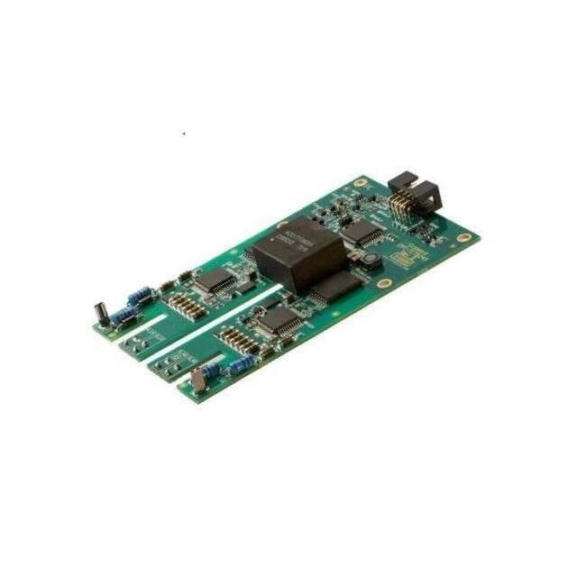
• Board size: 69 mm * 116 mm
• Low inductance gate loop design
• Operating temperature: -40°C to
125°C
• Single power supply: 12V-18V
• Bus voltage:1200V/1700V max
• Open-drain fault output
• Isolation: 3600VAC @50Hz (1min)
• Under voltage lockout (UVLO)
• 14mm Creepage/12mm clearance
• On-board optional non-overlap
generation (via jumper)
• RS422 PWM input interface
• > 50kV/µs dV/dt immunity
• Low parasitic capacitance between
primary and high-side: 10pF
• Switching frequency up to 100kHz
• Delay (PWM to VOUT): 200ns typ.
• FET Gate rise/fall time:40ns typ.
• Anti-overlap protection (on PWM
inputs)
• Glitch suppressor on PWM inputs
• Active Miller Clamping (AMC)
• Desaturation protection
• Gate-Source short-circuit protection
Note1: Please always refer to the latest datasheet version available at:
http://www.cissoid.com/files/files/products/titan/CMT-TIT8243.pdf
PUBLIC
Doc. PDS-181985 V1.4
WWW.CISSOID.COM
8-Jan-21
1 of 15
�1200V/1700V High Temperature (125°C) Half-Bridge SiC MOSFET Gate Driver
Preliminary Datasheet
Ordering Information
Product Name
CMT-TIT8243
CMT-TIT8244
Ordering Reference
CMT-TIT8243A
CMT-TIT8244A
Voltage
1200V
1700V
Marking
CMT-TIT8243A
CMT-TIT8244A
High level block diagram
CMT8243/8244
D_HS
DESAT
VH_HS
VREF
VH_HS
VREF
UVLO
VL_HS
HS
FAULTH
RGPH
UVLO
PWMHP/PWMHN
Primary
logic
Secondary
Logic
Isolated Data Transceiver
G_HS
DESAT
RGNH
LS
VH_HS
VIN
S_HS
VL_HS
S_HS
DC/DC
PWM
PWM
PWM
Controller
CONTROLLER
VL_HS
VH_LS
D_LS
S_LS
DESAT
VH_LS
VREF
GND
VL_LS
VH_LS
VREF
UVLO
VL_LS
HS
RGPL
UVLO
G_LS
FAULTL
PWMLP/PWMLN
DESAT
Primary
logic
LS
Isolated Data Transceiver
PUBLIC
Doc. PDS-181985 V1.4
RGNL
Secondary
Logic
WWW.CISSOID.COM
VL_LS
S_LS
8-Jan-21
2 of 15
�1200V/1700V High Temperature (125°C) Half-Bridge SiC MOSFET Gate Driver
Preliminary Datasheet
IO Description2
Pin Name
Pin ID
Pin Description
PMWLN
1
PWMHN
2
PMWLP
3
PWMHP
4
FAULTL
5
Low-side fault
FAULTH
6
High-side fault
GND
7
Ground
VIN
8
Positive supply
Negative Low-side PWM control signal
Negative High-side PWM
control signal
Positive Low-side PWM control signal
Positive High-side PWM control signal
PE
Chassis connection
D_HS
High-side drain sense signal
G_HS
High-side gate signal
S_HS
High-side source sense signal
S_LS
Low-side source sense signal
G_LS
Low-side gate signal
D_LS
Low-side drain sense signal
VIN
GND
PWMHP/PWMHN
FAULTH
PWMLP/PWMLN
FAULTL
PE
2
Positive supply
All other power supplies for driving the gate of the FETs are internally generated
by the on-board DC-DC converter
Ground
Reference ground for the supply and the digital IOs.
Input control signals for the high-side driver
These signals control the state of the high-side FET.
When in Local mode (selection by jumper), those signals control both low-side
and high-side channels in opposite states with some internally defined nonoverlapping delay.
High-side channel fault output (open drain)
This signal combines:
The high-side secondary Desaturation fault
The high-side secondary UVLO fault
The primary fault.
In case of fault, FAULTH is set to “0V” for a duration equal to internal timer defined at board level.
Input control signal for the low-side driver
The signal controls the state of the low-side FET.
When in Local mode (selection by jumper), those signals have no effect, the
low-side FET being control by PWMH and the local non-overlap function.
Low-side channel fault output (open drain)
This signal combines:
The low-side secondary Desaturation fault
The low-side secondary UVLO fault
The primary fault.
In case of fault, FAULTL is set to “0V” for a duration equal to internal timer defined at board level.
Chassis connection
A 1000V 1nF capacitance is connected between PE and each of the pins 1 to 8
Refer to section Mechanical characteristics page 13 for more details on connector pinout
PUBLIC
Doc. PDS-181985 V1.4
WWW.CISSOID.COM
8-Jan-21
3 of 15
�1200V/1700V High Temperature (125°C) Half-Bridge SiC MOSFET Gate Driver
Preliminary Datasheet
Absolute Maximum Ratings
Stressing the board above these absolute maximum ratings could present permanent damage. Exposure to this maximum rating for extended periods may affect the board reliability.
These ratings are considered individually (not in combination). If not specified, voltages are
related to GND
Parameter
(VIN-GND)
Voltage transient on S_HS
Voltage on D_HS, D_LS
Output power per gate
Steady Operating Temperature (no airflow)
Storage Temperature
Min.
-0.5
-40
-40
PUBLIC
Doc. PDS-181985 V1.4
WWW.CISSOID.COM
Max.
18
100
1200/1700
2.375
125
125
Units
V
kV/µs
V
W
°C
°C
8-Jan-21
4 of 15
�1200V/1700V High Temperature (125°C) Half-Bridge SiC MOSFET Gate Driver
Preliminary Datasheet
Electrical Characteristics
Unless otherwise stated: Tj=25°C. Bold underlined values indicate values valid
over the whole temperature range (-40°C < Ta < +125°C).
Parameter
Condition
Min
Typ
Max
Units
External Power Supply
External Power Supply
VIN
IAVG(VIN)
IAVG(VIN) max
Parameter
Versus GND
12
VIN=12V, no PWM
No fault situation
Direct Mode
Load: CREE WOLFSPEEDCAS300M12BM2
VIN=12V; 20 kHz; 50% DutyCycle
No fault situation
Direct Mode
Load: CREE WOLFSPEEDCAS300M12BM2
VIN=12V
Condition
18
103
mA
220
mA
500
Min
V
Typ
Max
mA
Units
Isolation
Inter channel Isolation
IH2L
Low-side channel isolation
IL2P
High-side channel isolation
IH2P
Maximum supported dV/dt
Parasitic capacitance
Creepage
Clearance
S_HS to S_LS
(50Hz, 1min)
S_LS to GND
(50Hz, 1min)
S_HS to GND
(50Hz, 1min)
S_HS to S_LS
S_HS to GND
(guaranteed by design)
Between High-Side and Primary
Primary to any secondary
Between secondaries
Primary to any secondary
Between secondaries
PUBLIC
Doc. PDS-181985 V1.4
WWW.CISSOID.COM
3.6
kVrms
3.6
kVrms
3.6
kVrms
50
kV/µs
14
10
pF
mm
12
mm
8-Jan-21
5 of 15
�1200V/1700V High Temperature (125°C) Half-Bridge SiC MOSFET Gate Driver
Preliminary Datasheet
Electrical Characteristics
Unless otherwise stated: Tj=25°C. Bold underlined values indicate values valid
over the whole temperature range (-40°C < Ta < +125°C).
Parameter
Condition
Min
Typ
Max
Units
PWML/PWMH inputs
Common mode input level
-6
Differential input high-threshold voltage
Diff(PWMxP,PWMxN)
Differential input low-threshold voltage
Differential input impedance
Diff(PWMxP,PWMxN)
Minimum pulse width
Anti-overlap duration
Propagation
delay
(PWML/PWMH
→G_LS/G_HS) (50% to 10%)
Non-overlap duration3
200
mV
Ω
50
ns
200
ns
100
100
0
Direct Mode
Default settings for glitch suppressor
and anti-overlap prevention
Local Mode (configurable via capacitance Cnovd)
V
mV
-50
Configurable via capacitances Cglil (on
PWML) and Cglih (on PWMH)
Direct Mode
Configurable via capacitances Cnovl
(on PWML) and Cnovh (on PWMH)
Maximum frequency
Duty cycle
+10
200
kHz
%
170
ns
480
ns
FAULTL/FAULTH open drain outputs
On resistance
Fault local latching time (at Primary or at
Secondary)
Parameter
G_LS/G_HS Gate driver outputs
High level
Low level
Maximum average output load current
Peak output current
Rgate_on
Rgate_off
Gate-Source resistance
Active Miller Clamp (AMC) transistor
Rdson
Applies to FAULTL/FAULTH
25
14
Condition
Rgate_on=Rgate_off= 0Ω
Ω
ms
Min
Typ
Max
Units
19.4
-5.2
20
-5
20.6
-4.8
95
1.8
1.8
100
V
V
mA
A
Ω
Ω
kΩ
33
mΩ
10
D_LS/D_HS Desaturation Monitoring inputs
Voltage range
CMT8243
CMT8244
0
0
Parameter
Condition
Min
Typ
Under-voltage Lockout on primary supply (VIN) (UVLO_P)
UVLO_P High Threshold
9.75
UVLO_P Low Threshold
8.2
Under-voltage Lockout on secondary supplies (VDD_L-VSS_L)/ (VDD_H-VSS_H) (UVLO_S)
UVLO_S High Threshold
22.7
UVLO_S Low Threshold
20.5
Desaturation detection
Threshold on D_LS/D_HS
D_LS/D_HS wrt to S_LS/S_HS
4.34
(configurable via resistance Rdesatx)
Configurable via capacitance Cdesatdx
Desaturation Blanking time
1
(68pF Cdesatdx installed)
Delay from desaturation detection to
350
G_LS/G_HS starting to turn off
G_LS/G_HS turn-off time after desatura- From 20V to 0V
tion detection
Load : CREE WOLFSPEED1
CAS300M12BM2
Soft Shutdown (SSD) resistor
20
Start-up
Start-up time
30
3
1200
1700
V
V
Max
Units
V
V
V
V
V
µs
ns
µs
Ω
ms
Non-overlap delay includes glitch suppressor delay; 10pF parasitic capacitance to be added to Cnovd
PUBLIC
Doc. PDS-181985 V1.4
WWW.CISSOID.COM
8-Jan-21
6 of 15
�1200V/1700V High Temperature (125°C) Half-Bridge SiC MOSFET Gate Driver
Preliminary Datasheet
Circuit Functionality
Description
Under-Voltage Lockout (UVLO)
CMT-TIT8243/8244 board is a Half-Bridge
gate driver board meant to drive 62mm
SiC power modules (typically CREE
WOLFSPEED CAS300M12BM2).
CMT-TIT8243/8244 board monitors constantly:
-
Its main features are:
-
-
-
-
-
-
-
-
-
Isolated data transmission (robust to
high dV/dt) (data and fault) on both
high and low side channels
Adjustable fault timer with automatic
restart
Safe start-up sequence through monitoring of the main supply (UVLO) and
of the voltage regulators output
(through Power-Good function)
Permanent and programmable Under-Voltage Lockout (UVLO) monitoring on external and internally generated power switch supplies
Desaturation detection function with
programmable blanking time and
threshold protecting power switches
in case of abnormal current levels
Soft-Shutdown transistor and control
performing power device graceful
shutdown in case of fault and so preventing too high dI/dt in the power
stage
Active Miller Clamping (AMC)
Flyback DC-DC convertor with cycleby-cycle current limit for short circuit
protection
High-precision (typ 3%) high-level
gate voltage generation
Differential RS422 PWM inputs
Open-drain low-ohmic (typ. 25Ω)
FAULT output
Support of 2 separate incoming PWM
channels and of locally generated
non-overlapped PWM signals
Configurable 50ns (typ) spike filter on
incoming PWM signal for enhanced
noise robustness
Configurable 200ns (typ) anti-overlap
protection on incoming PWM signals
Gate-2-Source short-circuit protection
At primary side, the monitored power supply is “VIN-GND”; to avoid oscillation when
(VIN-GND) is close to the UVLO threshold,
a hysteresis is implemented.
At each secondary side, the monitored
power
supply
is
“VDD_L-VSS_L”/
“VDD_H-VSS_H”; to avoid oscillation
when (VDD_x-VSS_x) is close to the
UVLO threshold, a hysteresis is implemented.
Refer to the chapter Fault Management/LED status for details about fault
behavior and management.
On-board power supplies
The on-board isolated power supply is a
regulated flyback DC-DC converter providing both channels with the positive and
negative supply voltages required to drive
the power FETs. It offers high voltage isolation between the channels, high dV/dt
sustainability and very low parasitic capacitance. Cycle-by-cycle current monitoring
at primary side is implemented to protect
the board against short-circuit.
High accuracy (typ 3%) is achieved on all
secondary positive supplies.
Interface towards controller
PWM inputs
PWML and PWMH input interface is based
on RS422 differential receivers to increase
noise immunity on those incoming signals.
are high impedance inputs.
CMT-TIT8243/8244 board implements 2
protection functions on the PWM data
paths:
PUBLIC
Doc. PDS-181985 V1.4
VIN power supply
High-side secondary supplies (typ
+20V/-5V)
Low-side secondary supplies (typ
+20V/-5V)
WWW.CISSOID.COM
8-Jan-21
7 of 15
�1200V/1700V High Temperature (125°C) Half-Bridge SiC MOSFET Gate Driver
Preliminary Datasheet
- Anti-glitch: any negative or positive
glitch on PWML/PMWH signals smaller
than a programmed value is ignored by
the board; this is increasing immunity of
incoming signals against external
noise; the signals are delayed by the
corresponding anti-glitch time
tMINPW (ns)= 0.5* [CGLIx (pF)]
- Anti-overlap: this circuit prevents
PWML and PMWH to be active at the
same time by forcing an internal nonoverlap time; if PWML and PWMH are
not overlapping by more than the internally programmed time, they are not
delayed internally. If PWML and PWMH
are active for a long period, both gate
outputs are forced to zero until one of
the inputs goes to zero.
tNOVP (ns)= 0.5* [CNOVx (pF)]
The sensing of the power device drain
voltage is performed through a high voltage sensing diode whom cathode is connected to the power switch drain and
whom anode is connected to a current
source (typ 2mA) and a sensing circuit.
The
desaturation
threshold
(on
D_LS/D_HS nodes) is configured by onboard resistors and can be tuned according to the table below.
Rdesat value
0KΩ
5KΩ
10KΩ (default)
15KΩ
20KΩ
30KΩ
Desat threshold (V)
25°C
125°C
0.93
1.22
2.35
2.62
3.77
4.02
5.18
5.42
6.6
6.82
9.42
9.62
At system level, the de-saturation detection should only be taken into account after a defined time following the low-to-high
transition on the power device gate. This
“blanking” time tDESAT_D is implemented
and adjusted by an on-board capacitor
CDESATD (68pF installed) and can be calculated as follows:
tDESATD (ns)= 14* [CDESATD (pF) + 7]
FAULT outputs
The output buffers operate as an opendrain driver with a low Ron resistance (typ.
25Ω), enabling the use of low value pull-up
resistance for increased noise immunity.
Isolated data transmission
CMT-TIT8243/8244 board uses integrated
digital isolators. Those devices provide
isolation, immunity against high dV/dt and
low parasitic capacitance.
In case no power supply is present at the
secondary side, a fault is generated at the
primary side.
Desaturation detection
The purpose of the desaturation function is
to detect that the voltage at the drain of
the power switch, in “ON” state, is higher
than a given threshold. This informs the
logic part of the system about possible
damage of the power arm (e.g. a short
circuit at the arm level leading to an overcurrent in the power switch).
If after tDESAT_D time, the DESAT comparator output indicates that D_LS/D_LS level
is higher than the programmed threshold
value, an internal DESAT fault is generated. Refer to the chapter Fault Management/LED status for details about fault
behavior and management.
When the desaturation fault is detected,
the power module gate is gracefully discharged thanks to the Soft-Shutdown circuit to avoid high dI/dt at power module
turn-off
To sense the drain voltage, fast-on connectors are present on the board (see
them marked D_HS, D_LS on picture below). For D_LS signal sensing, instead of
a wire towards the power module, a wire
between D_LS net and S_HS net (see
wire in red on picture below) can be added
by the customer; this can simplify the wiring towards the power module.
PUBLIC
Doc. PDS-181985 V1.4
WWW.CISSOID.COM
8-Jan-21
8 of 15
�1200V/1700V High Temperature (125°C) Half-Bridge SiC MOSFET Gate Driver
Preliminary Datasheet
Active Miller Clamping
In case of high positive dV/dt and despite
the negative drive of the power module
gate, a parasitic turn-on of the gate could
take place, inducing shoot-through current
on the power arm.
To prevent this, CMT-TIT8243/8244 board
implements an Active Miller Clamping
function by bypassing the gate resistance
with a low ohmic path (implemented with a
transistor) when the gate is driven negative.
This transistor also helps to limit the amplitude of negative kick on the power module
gate in case of negative dV/dt.
Fault Management/LED status
At primary side, fault is generated by any
of those situations:
-
Main power supply (VIN) is below
the UVLO threshold
Primary linear voltage regulator
(generating the 5V output required
by the on-board logic) is below the
internal Power Good level
Those faults are internally combined to
generate a unique fault signal. This internal fault signal is latched for 14msec.
While the fault is latched:
-
Both FAULTL/FAULTH pins are tied
to “0”
Both power switches are turned off
On board DC-DC converter is off
After the predefined latch time period,
CMT-TIT8243/8244 board will attempt to
return to normal operation:
- If the fault is still present, CMTTIT8243/8244 board will stay in the
fault state till the fault disappears
- If the fault disappeared (e.g. temporary
UVLO
situation),
CMTTIT8243/8244 board will go out of
FAULT state and return to normal
operation (DC-DC converter turned
on and data paths active); still, on
the PWM path, transition to normal
operation will happen on the next
positive edge of the incoming PWM
signal.
The primary fault state is combined with
the faults returned by the secondary devices according to Table 1.
Prim
fault
Lowside
fault
No
Yes
No
Yes
Yes or
No
No
No
No
No
Yes
FAULTL
FAULTH
No fault
Fault
No fault
Fault
Fault
No fault
No fault
Fault
Fault
Fault
Table 1: FAULT aggregation table
At each of the secondary side, fault is
generated by any of those situations:
-
-
Power supply is below the UVLO
threshold
Secondary voltage regulator (5V)
output voltage is below the PowerGood threshold
Desaturation situation is detected
by the DESAT comparator
Those faults are internally combined to
generate a unique fault signal. This internal fault signal is latched for 14msec.
While the fault is latched, the gate driver is
turned off. At the transition between “no
fault” and “fault” situation, the gate driver
circuit is gracefully shut down (Soft ShutDown).
After the predefined latch time period, the
gate driver circuit returns to normal operation:
-
-
If the fault is still present, the gate
driver is kept turned off till the fault
disappears
If the fault disappeared (e.g. temporary UVLO situation), normal
operation will resume on the next
positive edge of incoming PWM
signal
2 LEDs are present on the CMTTIT8243/8244 board and are reflecting
board status as follows:
State
No supply
Operational
Primary
or
secondary
fault
PUBLIC
Doc. PDS-181985 V1.4
Highside
fault
No
No
Yes
Yes
Yes or
No
WWW.CISSOID.COM
LED1
State
Off
On
On
Color
None
Green
Green
LED2
State
Off
Off
On
Color
None
None
Red
8-Jan-21
9 of 15
�1200V/1700V High Temperature (125°C) Half-Bridge SiC MOSFET Gate Driver
Preliminary Datasheet
Modes of operation
Board power dissipation
CMT-TIT8243/8244 board offers 2 modes
of operation:
Current consumption of the CMTTIT8243/8244 board (Vin=12V) can be
computed as follows:
-
-
Direct Mode: PWML and PWMH
are generated independently outside CMT-TIT8243/8244 board. In
this case, proper non overlapping
must be generated externally.
Local Mode: PWML and PWMH
are generated out of one input
signal (PWMH) and proper non
overlapping timing is managed locally on the CMT-TIT8243/8244
board (cfr Figure 1)
Iin = 103mAtyp +
Act * (0.26 + 0.0055 * Qg ) * Fs
Where:
-
-
PWMH
-
NGH
NGL
tNOV_D
tNOV_D
Figure 1: Local Mode operation
The choice between those 2 modes of operation is made via the jumper JP1.
When in Local Mode, an on-board capacitance (Cnovd) defines the non-overlap
delay according to following formula:
Iin is the input current (in mA) (wrt to
Vin = 12V)
Act is a Boolean (0: PWML/PWMH =
0, 1: PWM_L/PWM_H alternating at
Fs frequency)
Gg: Total gate charge of one power
transistor (in nC)
Fs: Switching frequency (in kHz)
The duty cycle of the PWML/PWMH signals has almost no influence on the current
consumption
of
the
CMTTIT8243/8244 board (assuming PWML
and PWMH duty cycles are complementary).
To stay within specifications of the internal
secondary voltages, the maximum average Iin current should be 500 mA (for Vin
=12V).
tNOV_D (ns)=5.5 * CNOVD (pF)
PUBLIC
Doc. PDS-181985 V1.4
WWW.CISSOID.COM
8-Jan-21
10 of 15
�1200V/1700V High Temperature (125°C) Half-Bridge SiC MOSFET Gate Driver
Preliminary Datasheet
Dynamic behavior
Figure 2 illustrates the CMT-TIT8243/8244 low-side driver dynamic behavior in normal operation and fault conditions.
Normal
Case
PWML
1
Fault
UVLO
Normal
Case
6
2
7
G_LS
UVLO
3
FAULT
Internal timer
4
Normal
Case
PWML
1
tFLTD
5
FAULT
Desat
Normal
Case
3
7
8
G_LS
D_LS
tDESATD
DESAT
BLANK tDESATD
FAULT
2
4
Internal timer
5
tFLTD
6
Figure 2: Timing diagram CMT-TIT8243/8244 low-side driver behaviour
In Normal operation
on PWML rising edge (1), rising edge is
generated on G_LS (after propagation delay through CMT-TIT8243/8244 board).
After rising edge on G_LS, low-side power
module is turned ON and midpoint node is
going to “0” state (voltage equals to Ron *
current flowing through the power device).
D_LS node is also pulled down and after
blanking time (tDESAT_D), no desaturation
fault is detected and FAULTL remains
high.
on PWML falling edge (2), falling edge is
generated on G_LS (after propagation delay through CMT-TIT8243/8244 board)
After falling edge on G_LS, the low-side
power device is turned OFF.
After rising edge on G_LS, low-side power
module is turned ON; because of a desaturation fault, D_LS node does not reach its
normal “0” level. Thanks to the DESAT
comparator, CMT-TIT8243/8244 board
detects this fault situation and turns off
gracefully G_LS. Power device is turned
off. FAULTL signal is pulled down. Fault is
cleared after fault timer expiry.
In UVLO fault situation
UVLO status is monitored inside the secondary devices (and inside primary device
as well; for clarity, only secondary UVLO
situation is described here). When UVLO
comparator (5) detects an under-voltage
situation, G_LS is gracefully shut down
FAULTL signal is pulled down. Fault is
cleared after fault timer expiry.
In DESAT fault situation
on PWML rising edge (3), rising edge is
generated on G_LS (after propagation delay through CMT-TIT8243/8244 board)
PUBLIC
Doc. PDS-181985 V1.4
WWW.CISSOID.COM
8-Jan-21
11 of 15
�1200V/1700V High Temperature (125°C) Half-Bridge SiC MOSFET Gate Driver
Preliminary Datasheet
Settings Management
Function
Position
on PCB
Direct/Local
Mode
Non-overlap
time
P1
Component location
Settings
Jumper not present: Direct
mode
Jumper present: Local mode
Cnovd (top)
tNOV_D (ns)=5.5 * CNOVD (pF)
Desaturation
threshold
Desaturation
blanking time
Component
name
JP2 (top)
Rdesat2h-A
P2
Cfr section Desaturation detection
Cdesath-A
Top view
Bottom view
PUBLIC
Doc. PDS-181985 V1.4
WWW.CISSOID.COM
8-Jan-21
12 of 15
�1200V/1700V High Temperature (125°C) Half-Bridge SiC MOSFET Gate Driver
Preliminary Datasheet
Mechanical characteristics
Top view
Bottom view
PUBLIC
Doc. PDS-181985 V1.4
WWW.CISSOID.COM
8-Jan-21
13 of 15
�1200V/1700V High Temperature (125°C) Half-Bridge SiC MOSFET Gate Driver
Preliminary Datasheet
Mechanical characteristics (cnt’d)
Side view
Front view
PUBLIC
Doc. PDS-181985 V1.4
WWW.CISSOID.COM
8-Jan-21
14 of 15
�1200V/1700V High Temperature (125°C) Half-Bridge SiC MOSFET Gate Driver
Preliminary Datasheet
Contact
CISSOID S.A.
Headquarters and
contact EMEA:
CISSOID S.A. – Rue Francqui, 3 – 1435 Mont Saint Guibert - Belgium
T : +32 10 48 92 10 - F: +32 10 88 98 75
Email: sales@cissoid.com
Sales
Representatives:
Visit our website: http://www.cissoid.com
Disclaimer
Neither CISSOID, nor any of its directors, employees or affiliates make any representations or extend any warranties
of any kind, either express or implied, including but not limited to warranties of merchantability, fitness for a particular
purpose, and the absence of latent or other defects, whether or not discoverable. In no event shall CISSOID, its directors, employees and affiliates be liable for direct, indirect, special, incidental or consequential damages of any kind
arising out of the use of its circuits and their documentation, even if they have been advised of the possibility of such
a damage. The circuits are provided “as is”. CISSOID has no obligation to provide maintenance, support, updates, or
modifications.
PUBLIC
Doc. PDS-181985 V1.4
WWW.CISSOID.COM
8-Jan-21
15 of 15
�