TS19375
PWM Step-Up Controller
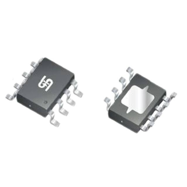
SOP-8
Pin Definition:
1. EN
8. NC
2. Vcc
7. GND
3. FB
6. Gate
4. SS
5. Sense
General Description
The TS19375 is high efficient PWM step-up controller. Designed to drive an external N-channel MOSFET, Output
voltage is programmable with 1.0V of standard voltage supply internal, and using externally connected
components, output voltage (FB) can be set up at will.
The TS19375 can be operated at switching frequencies of 500kHz allowing for easy filtering and low noise, the
size of the external components can be reduced. An enable function and thermal shutdown functions are built
inside. The soft-start time can be programmed by outside capacitor; the function prevents overshoot at startup.
Features
Ordering Information
●
Input voltage range 3V ~ 24V
●
Output voltage: Define by N-CH MOSFET
●
Duty ratio: 0% ~ 85% PWM control
●
Oscillation frequency: 500kHz
●
Soft-start time programmed by external capacitor
Application
●
Thermal shutdown protection
●
LED Panel Display Backlighting
●
Internal current limit
●
PDA and Portable Media Players
●
External SW N-CH MOSFET
●
Local Boost Regulator
Part No.
TS19375CS RLG
Package
SOP-8
Packing
2.5Kpcs / 13” Reel
Note: “G” denotes for Halogen Free
Typical Application Circuit
VOUT=VFB x (1+R1/R2), VFB=1V, R2=1k~3k
C4 Capacitor ESR suggest 30mΩ ~ 100mΩ
1/8
Version: C12
�TS19375
PWM Step-Up Controller
Absolute Maximum Rating
Characteristics
Symbol
Rating
Unit
VCC
VFB
VEN
VSENSE
VSS
VGATE
PD
TSTG
TOPJ
VOP
θJC
θJA
VSS - 0.3 to VSS + 26
VSS - 0.3 to 12
VSS - 0.3 to VCC
VSS - 0.3 to VCC
VSS - 0.3 to VCC
VSS - 0.3 to VCC
Internally limited
-40 to +150
-20 to +125
+3 to +24
40
120
V
V
V
V
V
V
mW
ºC
ºC
V
ºC/W
ºC/W
VCC Pin Voltage
Feedback Pin Voltage
EN Voltage
SENSE Voltage
SS Pin Voltage
Gate Pin Voltage
Power Dissipation
Storage Temperature Range
Operating Junction Temperature Range
Operating Supply Voltage
Thermal Resistance from Junction to case
Thermal Resistance from Junction to ambient
Note: Stresses exceed those rating may damage the device
Electrical Specifications (TA=25oC, VIN=5V, VOUT=12V unless otherwise noted)
Characteristics
Symbol
Conditions
Min
Typ
Max Units
Feedback Voltage
VFB
IOUT=0.1A
Quiescent Current
ICCQ
VFB=1.5V force driver off
-
4
6
mA
0.975 1.000 1.025
V
Feedback Bias Current
IFB
IOUT=0.1A
-
0.1
0.5
uA
Shutdown Supply Current
ISD
VEN =0V
-
1
10
uA
FOSC
SW pin
400
500
600
KHz
0.05
0.06
0.07
V
-
8
-
uA
Oscillation Frequency
Sense Voltage
Soft Start Current
EN Pin Logic input threshold voltage
EN Pin Input Current
VSENSE
ISS
VSS=0V
VSH
High (regulator ON)
2.0
-
-
VSL
Low (regulator OFF)
-
-
0.8
ISH
VEN=2.5V (ON)
-
20
-
uA
ISL
VEN=0.3V (OFF)
-
-1
-
uA
LX Rise Time
TLXR
CLX=1000pF
-
60
-
LX Fall Time
TLXF
CLX=1000pF
-
60
-
Efficiency
EFFI
VCC = 5V,
VOUT = 12V
-
91
-
IOUT = 1A
Maximum Duty Cycle
DCMAX
VFB=0V
-
85
-
Minimum Duty Cycle
DCMIN
VFB=1.5V
-
0
-
-
145
-
Thermal shutdown Temp
TSD
2/8
V
nS
%
%
°C
Version: C12
�TS19375
PWM Step-Up Controller
Block Diagram
Vcc
Phase
Compensation
FB
Regulator
+
+
-
Vref=1.0V
Buffer
Driver
PWM
Controller
EN
Oscillator
8uA
VEN
GATE
GND
Thermal
Shutdown
0.06V
SS
SENSE
Pin Function Description
Pin NO. Pin Name
Pin Description
1
EN
Shutdown Control Input
H: Normal Operation
L: Shutdown Mode
2
VCC
VCC Supply pin
3
FB
Feedback Pin
4
SS
Soft-Start pin
5
VSENSE
6
Gate
Gate drive for external N-CH MOSFET
7
GND
Signal Ground Pin
8
NC
Current Limit Sense Voltage
Non Connect
3/8
Version: C12
�TS19375
PWM Step-Up Controller
Function Description
PWM Control
The TS19375 is high efficient PWM step-up controller, the pulse width varies in a range from 0 to 85%. According
to the load current, the ripple voltage produced by the switching can easily be removed through a filter because the
switching frequency remains constant. Therefore, TS19375 provide a low-ripple power over broad ranges of input
voltage and load current.
Setting the Output Voltage
Application circuit shows the basic application circuit with adjustable output version. The external resistor sets the
output voltage according to the following formula:
Table 1: Resistor select for output voltage setting
VOUT
R2
R1
12V
1K
11K
15V
1.5K
21K
18V
1K
17K
24V
1.3K
30K
Current Limit Setting
The current limit threshold is setting by the external resistor (RSENSE) connecting from SENSE pin to GND (refer the
application circuit). The internal current limit compared voltage is 60mV. When the SENSE voltage is larger than
60mV, an over-current condition is triggered. Please refer to the formula for setting the minimum current limit value:
Note: ISW(MAX) is the maximum N-MOSFET current
Inductor Selection
For most designs, Low inductance values are physically smaller but require faster switching, which results in some
efficiency loss. The inductor value can be derived from the following formula:
Large value inductors lower ripple current and small value inductors result in high ripple currents. Choose inductor
ripple current approximately 15% of the maximum input current 3A, ∆IL=0.45A.
Table 2: Inductor select for output voltage setting (VCC=5V)
VOUT
9V
12V
15V
18V
L1 Value
18uH
15uH
10uH
10uH
The DC current rating of the inductor should be at least equal to the maximum load current plus half the ripple
current to prevent core saturation (3A+0.25A).
4/8
Version: C12
�TS19375
PWM Step-Up Controller
Function Description (Continue)
Input Capacitor Selection
The input capacitor reduces the surge current drawn from the input and switching noise from the device. The input
capacitor impedance at the switching frequency shall be less than input source impedance to prevent high
frequency switching current passing to the input. A low ESR input capacitor sized for maximum RMS current must
be used.
The capacitor voltage rating should be at least 1.5 times greater than the input voltage, and often much higher
voltage ratings are needed to satisfy.
Output Capacitor Selection
The output capacitor is required to keep the output voltage ripple small and to ensure regulation loop stability. The
output capacitor must have low impedance at the switching frequency. A low ESR capacitor sized for maximum
RMS current must be used. The low ESR requirements needed for low output ripple voltage. The capacitor voltage
rating should be at least 1.5 times greater than the input voltage, and often much higher voltage ratings are needed
to satisfy.
The ESR range of output capacitor is 30m~100mΩ at switch current more than 1.5A. Add a 4.7uF output bypass
capacitor in order to reduce output ripple effectively
5/8
Version: C12
�TS19375
PWM Step-Up Controller
Electrical Characteristics Curve (TA=25ºC, VIN=5V, VFORWARD-LED=3.3V, unless otherwise noted)
Input Voltage vs. Output Voltage
Output Current vs. Output Voltage
Shutdown Current vs. Temperature
Feedback Voltage vs. Temperature
6/8
Version: C12
�TS19375
PWM Step-Up Controller
SOP-8 Mechanical Drawing
DIM
A
B
C
D
F
G
K
M
P
R
SOP-8 DIMENSION
MILLIMETERS
INCHES
MIN
MAX
MIN
MAX.
4.80
5.00
0.189
0.196
3.80
4.00
0.150
0.157
1.35
1.75
0.054
0.068
0.35
0.49
0.014
0.019
0.40
1.25
0.016
0.049
1.27BSC
0.05BSC
0.10
0.25
0.004
0.009
0º
7º
0º
7º
5.80
6.20
0.229
0.244
0.25
0.50
0.010
0.019
Marking Diagram
Y = Year Code
M = Month Code for Halogen Free Product
(O=Jan, P=Feb, Q=Mar, R=Apl, S=May, T=Jun, U=Jul, V=Aug,
W=Sep, X=Oct, Y=Nov, Z=Dec)
L = Lot Code
7/8
Version: C12
�TS19375
PWM Step-Up Controller
Notice
Specifications of the products displayed herein are subject to change without notice. TSC or anyone on its behalf,
assumes no responsibility or liability for any errors or inaccuracies.
Information contained herein is intended to provide a product description only. No license, express or implied, to
any intellectual property rights is granted by this document. Except as provided in TSC’s terms and conditions of
sale for such products, TSC assumes no liability whatsoever, and disclaims any express or implied warranty,
relating to sale and/or use of TSC products including liability or warranties relating to fitness for a particular purpose,
merchantability, or infringement of any patent, copyright, or other intellectual property right.
The products shown herein are not designed for use in medical, life-saving, or life-sustaining applications.
Customers using or selling these products for use in such applications do so at their own risk and agree to fully
indemnify TSC for any damages resulting from such improper use or sale.
8/8
Version: C12
�
很抱歉,暂时无法提供与“TS19375CS RLG”相匹配的价格&库存,您可以联系我们找货
免费人工找货- 国内价格 香港价格
- 2500+7.879232500+0.95013
- 5000+7.587425000+0.91494


 工商网监
湘ICP备2023018690号
工商网监
湘ICP备2023018690号
