����������
���
�
� ��
��� �� ��
��� ���� ��
�������
���
����
SCHS340B − MARCH 2003 - REVISED JUNE 2003
D Inputs Are TTL-Voltage Compatible
D Speed of Bipolar F, AS, and S, With
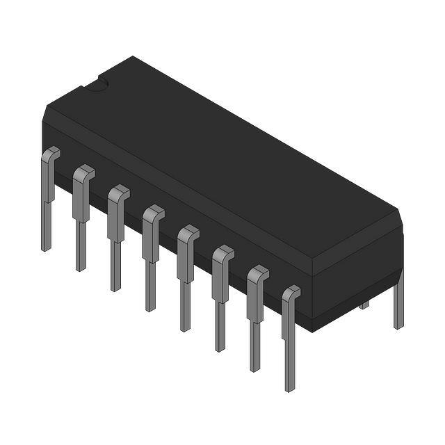
E, M, OR PW PACKAGE
(TOP VIEW)
Significantly Reduced Power Consumption
A /B
1A
1B
1Y
2A
2B
2Y
GND
D Balanced Propagation Delays
D ±24-mA Output Drive Current
D
D
− Fanout to 15 F Devices
SCR-Latchup-Resistant CMOS Process and
Circuit Design
Exceeds 2-kV ESD Protection Per
MIL-STD-883, Method 3015
1
16
2
15
3
14
4
13
5
12
6
11
7
10
8
9
VCC
G
4A
4B
4Y
3A
3B
3Y
description/ordering information
This quadruple 2-line to 1-line data selector/multiplexer is designed for 4.5-V to 5.5-V VCC operation.
The CD74ACT157 features a common strobe (G) input. When the strobe is high, all outputs are low. When the
strobe is low, a 4-bit word is selected from one of two sources and is routed to the four outputs. The device
provides true data.
ORDERING INFORMATION
PDIP − E
−55°C
−55
C to 125
125°C
C
ORDERABLE
PART NUMBER
PACKAGE†
TA
SOIC − M
TSSOP − PW
Tube
CD74ACT157E
Tube
CD74ACT157M
Tape and reel
CD74ACT157M96
Tube
CD74ACT157PW
Tape and reel
CD74ACT157PWR
TOP-SIDE
MARKING
CD74ACT157E
ACT157M
HM157
† Package drawings, standard packing quantities, thermal data, symbolization, and PCB design guidelines
are available at www.ti.com/sc/package.
FUNCTION TABLE
INPUTS
G
A/B
A
B
OUTPUT
Y
H
X
X
X
L
L
L
L
X
L
L
L
H
X
H
L
H
X
L
L
L
H
X
H
H
Please be aware that an important notice concerning availability, standard warranty, and use in critical applications of
Texas Instruments semiconductor products and disclaimers thereto appears at the end of this data sheet.
Copyright 2003, Texas Instruments Incorporated
����
����� ���� ����������� �! "#��$�� �! �� %#&'�"����� (��$)
���(#"�! "������ �� !%$"���"�����! %$� �*$ �$��! �� �$+�! ��!��#�$��!
!���(��( ,������-) ���(#"���� %��"$!!��. (�$! ��� �$"$!!���'- ��"'#($
�$!���. �� �'' %����$�$�!)
POST OFFICE BOX 655303
• DALLAS, TEXAS 75265
1
�����������
���
�
� ��
��� �� ��
��� ���� ��
�������
���
����
SCHS340B − MARCH 2003 - REVISED JUNE 2003
logic diagram (positive logic)
1A
2
4
3
1Y
1B
2A
5
7
2B
3A
6
11
9
3B
4A
10
G
A/B
3Y
14
12
4B
2Y
13
4Y
15
1
absolute maximum ratings over operating free-air temperature range (unless otherwise noted)†
Supply voltage range, VCC . . . . . . . . . . . . . . . . . . . . . . . . . . . . . . . . . . . . . . . . . . . . . . . . . . . . . . . . . . −0.5 V to 6 V
Input clamp current, IIK (VI < 0 V or VI > VCC) (see Note 1) . . . . . . . . . . . . . . . . . . . . . . . . . . . . . . . . . . . ±20 mA
Output clamp current, IOK (VO < 0 V or VO > VCC) (see Note 1) . . . . . . . . . . . . . . . . . . . . . . . . . . . . . . ±50 mA
Continuous output current, IO (VO > 0 V or VO < VCC) . . . . . . . . . . . . . . . . . . . . . . . . . . . . . . . . . . . . . . . ±50 mA
Continuous current through VCC or GND . . . . . . . . . . . . . . . . . . . . . . . . . . . . . . . . . . . . . . . . . . . . . . . . . . ±100 mA
Package thermal impedance, θJA (see Note 2): E package . . . . . . . . . . . . . . . . . . . . . . . . . . . . . . . . . . . 67°C/W
M package . . . . . . . . . . . . . . . . . . . . . . . . . . . . . . . . . . 73°C/W
PW package . . . . . . . . . . . . . . . . . . . . . . . . . . . . . . . . 108°C/W
Storage temperature range, Tstg . . . . . . . . . . . . . . . . . . . . . . . . . . . . . . . . . . . . . . . . . . . . . . . . . . . −65°C to 150°C
† Stresses beyond those listed under “absolute maximum ratings” may cause permanent damage to the device. These are stress ratings only, and
functional operation of the device at these or any other conditions beyond those indicated under “recommended operating conditions” is not
implied. Exposure to absolute-maximum-rated conditions for extended periods may affect device reliability.
NOTES: 1. The input and output voltage ratings may be exceeded if the input and output current ratings are observed.
2. The package thermal impedance is calculated in accordance with JESD 51-7.
2
POST OFFICE BOX 655303
• DALLAS, TEXAS 75265
�����������
���
�
� ��
��� �� ��
��� ���� ��
�������
���
����
SCHS340B − MARCH 2003 - REVISED JUNE 2003
recommended operating conditions (see Note 3)
−55°C to
125°C
TA = 25°C
−40°C to
85°C
UNIT
MIN
MAX
MIN
MAX
MIN
MAX
4.5
5.5
4.5
5.5
4.5
5.5
VCC
VIH
Supply voltage
VIL
VI
Low-level input voltage
Input voltage
0
VO
IOH
Output voltage
0
High-level output current
−24
IOL
∆t/∆v
Low-level output current
24
Input transition rise or fall rate
10
High-level input voltage
2
2
0.8
VCC
VCC
2
0.8
0
0
V
V
0.8
V
VCC
VCC
V
−24
−24
mA
24
24
mA
10
10
ns/V
VCC
VCC
0
0
V
NOTE 3: All unused inputs of the device must be held at VCC or GND to ensure proper device operation. Refer to the TI application report,
Implications of Slow or Floating CMOS Inputs, literature number SCBA004.
electrical characteristics over recommended operating free-air temperature range (unless
otherwise noted)
PARAMETER
TEST CONDITIONS
MIN
VOH
VI = VIH or VIL
VOL
VI = VIH or VIL
II
ICC
VI = VCC or GND
VI = VCC or GND,
DICC‡
VI = VCC − 2.1 V
−55°C to
125°C
TA = 25°C
VCC
MAX
MIN
−40°C to
85°C
MAX
MIN
UNIT
MAX
IOH = −50 µA
IOH = −24 mA
IOH = −50 mA†
4.5 V
4.4
4.4
4.4
4.5 V
3.94
3.7
3.8
IOH = −75 mA†
IOL = 50 µA
5.5 V
4.5 V
0.1
0.1
0.1
IOL = 24 mA
IOL = 50 mA†
IOL = 75 mA†
4.5 V
0.36
0.5
0.44
5.5 V
V
3.85
3.85
5.5 V
5.5 V
IO = 0
V
1.65
1.65
5.5 V
±0.1
±1
±1
µA
5.5 V
8
160
80
µA
2.4
3
2.8
mA
10
10
10
4.5 V to 5.5 V
Ci
pF
† Test one output at a time, not exceeding 1-second duration. Measurement is made by forcing indicated current and measuring voltage to minimize
power dissipation. Test verifies a minimum 50-Ω transmission-line drive capability at 85°C and 75-Ω transmission-line drive capability at 125°C.
‡ Additional quiescent supply current per input pin, TTL inputs high, 1 unit load
ACT INPUT LOADING TABLE
INPUT
UNIT LOAD
A or B
0.37
G
0.83
A/B
1.33
Unit load is ∆ICC limit specified in
electrical characteristics table
(e.g., 2.4 mA at 25°C).
POST OFFICE BOX 655303
• DALLAS, TEXAS 75265
3
�����������
���
�
� ��
��� �� ��
��� ���� ��
�������
���
����
SCHS340B − MARCH 2003 - REVISED JUNE 2003
switching characteristics over recommended operating free-air temperature range,
VCC = 5 V ± 0.5 V, CL = 50 pF (unless otherwise noted) (see Figure 1)
FROM
(INPUT)
TO
(OUTPUT)
tPLH
tPHL
A or B
Any Y
tPLH
tPHL
A/B
Any Y
tPLH
tPHL
G
Any Y
PARAMETER
−55°C to
125°C
−40°C to
85°C
MIN
MAX
MIN
MAX
2.4
9.5
2.5
8.6
2.4
9.5
2.5
8.6
3.6
14.5
3.8
13.2
3.6
14.5
3.8
13.2
3.4
13.5
3.6
12.3
3.4
13.5
3.6
12.3
UNIT
ns
ns
ns
operating characteristics, VCC = 5 V, TA = 25°C
PARAMETER
Cpd
4
Power dissipation capacitance
POST OFFICE BOX 655303
• DALLAS, TEXAS 75265
TYP
UNIT
156
pF
�����������
���
�
� ��
��� �� ��
��� ���� ��
�������
���
����
SCHS340B − MARCH 2003 - REVISED JUNE 2003
PARAMETER MEASUREMENT INFORMATION
S1
R1 = 500 Ω
From Output
Under Test
2 × VCC
Open
GND
CL = 50 pF
(see Note A)
R2 = 500 Ω
TEST
S1
tPLH/tPHL
tPLZ/tPZL
tPHZ/tPZH
Open
2 × VCC
GND
tw
3V
1.5 V
Input
LOAD CIRCUIT
1.5 V
0V
VOLTAGE WAVEFORMS
PULSE DURATION
CLR
Input
3V
Reference
Input
3V
1.5 V
1.5 V
0V
0V
trec
Data
Input
3V
1.5 V
CLK
th
tsu
1.5 V
10%
90%
90%
tr
0V
VOLTAGE WAVEFORMS
RECOVERY TIME
3V
1.5 V
10% 0 V
tf
VOLTAGE WAVEFORMS
SETUP AND HOLD AND INPUT RISE AND FALL TIMES
3V
Input
1.5 V
1.5 V
0V
tPLH
In-Phase
Output
50%
10%
90%
90%
tr
90%
1.5 V
1.5 V
0V
tPHL
tPHL
Out-of-Phase
Output
3V
Output
Control
VOH
50% VCC
10%
VOL
tf
tPLH
50% VCC
10%
tf
50%
10%
90%
VOH
VOL
tr
VOLTAGE WAVEFORMS
PROPAGATION DELAY AND OUTPUT TRANSITION TIMES
Output
Waveform 1
S1 at 2 × VCC
(see Note B)
tPLZ
tPZL
20% VCC
tPHZ
tPZH
Output
Waveform 2
S1 at GND
(see Note B)
≈VCC
20% VCC
VOL
80% VCC
VOH
80% VCC
≈0 V
VOLTAGE WAVEFORMS
OUTPUT ENABLE AND DISABLE TIMES
NOTES: A. CL includes probe and test-fixture capacitance.
B. Waveform 1 is for an output with internal conditions such that the output is low except when disabled by the output control.
Waveform 2 is for an output with internal conditions such that the output is high except when disabled by the output control.
C. All input pulses are supplied by generators having the following characteristics: PRR ≤ 1 MHz, ZO = 50 Ω, tr = 3 ns, tf = 3 ns.
Phase relationships between waveforms are arbitrary.
D. For clock inputs, fmax is measured with the input duty cycle at 50%.
E. The outputs are measured one at a time with one input transition per measurement.
F. tPLH and tPHL are the same as tpd.
G. tPZL and tPZH are the same as ten.
H. tPLZ and tPHZ are the same as tdis.
I. All parameters and waveforms are not applicable to all devices.
Figure 1. Load Circuit and Voltage Waveforms
POST OFFICE BOX 655303
• DALLAS, TEXAS 75265
5
�PACKAGE OPTION ADDENDUM
www.ti.com
18-Sep-2008
PACKAGING INFORMATION
Orderable Device
Status (1)
Package
Type
Package
Drawing
Pins Package Eco Plan (2)
Qty
CD74ACT157E
ACTIVE
PDIP
N
16
25
Pb-Free
(RoHS)
CU NIPDAU
N / A for Pkg Type
CD74ACT157EE4
ACTIVE
PDIP
N
16
25
Pb-Free
(RoHS)
CU NIPDAU
N / A for Pkg Type
CD74ACT157M
ACTIVE
SOIC
D
16
40
Green (RoHS &
no Sb/Br)
CU NIPDAU
Level-1-260C-UNLIM
CD74ACT157M96
ACTIVE
SOIC
D
16
2500 Green (RoHS &
no Sb/Br)
CU NIPDAU
Level-1-260C-UNLIM
CD74ACT157M96E4
ACTIVE
SOIC
D
16
2500 Green (RoHS &
no Sb/Br)
CU NIPDAU
Level-1-260C-UNLIM
CD74ACT157M96G4
ACTIVE
SOIC
D
16
2500 Green (RoHS &
no Sb/Br)
CU NIPDAU
Level-1-260C-UNLIM
CD74ACT157ME4
ACTIVE
SOIC
D
16
40
Green (RoHS &
no Sb/Br)
CU NIPDAU
Level-1-260C-UNLIM
CD74ACT157MG4
ACTIVE
SOIC
D
16
40
Green (RoHS &
no Sb/Br)
CU NIPDAU
Level-1-260C-UNLIM
CD74ACT157PW
ACTIVE
TSSOP
PW
16
90
Green (RoHS &
no Sb/Br)
CU NIPDAU
Level-1-260C-UNLIM
CD74ACT157PWE4
ACTIVE
TSSOP
PW
16
90
Green (RoHS &
no Sb/Br)
CU NIPDAU
Level-1-260C-UNLIM
CD74ACT157PWG4
ACTIVE
TSSOP
PW
16
90
Green (RoHS &
no Sb/Br)
CU NIPDAU
Level-1-260C-UNLIM
CD74ACT157PWR
ACTIVE
TSSOP
PW
16
2000 Green (RoHS &
no Sb/Br)
CU NIPDAU
Level-1-260C-UNLIM
CD74ACT157PWRE4
ACTIVE
TSSOP
PW
16
2000 Green (RoHS &
no Sb/Br)
CU NIPDAU
Level-1-260C-UNLIM
CD74ACT157PWRG4
ACTIVE
TSSOP
PW
16
2000 Green (RoHS &
no Sb/Br)
CU NIPDAU
Level-1-260C-UNLIM
Lead/Ball Finish
MSL Peak Temp (3)
(1)
The marketing status values are defined as follows:
ACTIVE: Product device recommended for new designs.
LIFEBUY: TI has announced that the device will be discontinued, and a lifetime-buy period is in effect.
NRND: Not recommended for new designs. Device is in production to support existing customers, but TI does not recommend using this part in
a new design.
PREVIEW: Device has been announced but is not in production. Samples may or may not be available.
OBSOLETE: TI has discontinued the production of the device.
(2)
Eco Plan - The planned eco-friendly classification: Pb-Free (RoHS), Pb-Free (RoHS Exempt), or Green (RoHS & no Sb/Br) - please check
http://www.ti.com/productcontent for the latest availability information and additional product content details.
TBD: The Pb-Free/Green conversion plan has not been defined.
Pb-Free (RoHS): TI's terms "Lead-Free" or "Pb-Free" mean semiconductor products that are compatible with the current RoHS requirements
for all 6 substances, including the requirement that lead not exceed 0.1% by weight in homogeneous materials. Where designed to be soldered
at high temperatures, TI Pb-Free products are suitable for use in specified lead-free processes.
Pb-Free (RoHS Exempt): This component has a RoHS exemption for either 1) lead-based flip-chip solder bumps used between the die and
package, or 2) lead-based die adhesive used between the die and leadframe. The component is otherwise considered Pb-Free (RoHS
compatible) as defined above.
Green (RoHS & no Sb/Br): TI defines "Green" to mean Pb-Free (RoHS compatible), and free of Bromine (Br) and Antimony (Sb) based flame
retardants (Br or Sb do not exceed 0.1% by weight in homogeneous material)
(3)
MSL, Peak Temp. -- The Moisture Sensitivity Level rating according to the JEDEC industry standard classifications, and peak solder
temperature.
Important Information and Disclaimer:The information provided on this page represents TI's knowledge and belief as of the date that it is
Addendum-Page 1
�PACKAGE OPTION ADDENDUM
www.ti.com
18-Sep-2008
provided. TI bases its knowledge and belief on information provided by third parties, and makes no representation or warranty as to the
accuracy of such information. Efforts are underway to better integrate information from third parties. TI has taken and continues to take
reasonable steps to provide representative and accurate information but may not have conducted destructive testing or chemical analysis on
incoming materials and chemicals. TI and TI suppliers consider certain information to be proprietary, and thus CAS numbers and other limited
information may not be available for release.
In no event shall TI's liability arising out of such information exceed the total purchase price of the TI part(s) at issue in this document sold by TI
to Customer on an annual basis.
Addendum-Page 2
�PACKAGE MATERIALS INFORMATION
www.ti.com
19-Mar-2008
TAPE AND REEL INFORMATION
*All dimensions are nominal
Device
Package Package Pins
Type Drawing
SPQ
Reel
Reel
Diameter Width
(mm) W1 (mm)
A0 (mm)
B0 (mm)
K0 (mm)
P1
(mm)
W
Pin1
(mm) Quadrant
CD74ACT157M96
SOIC
D
16
2500
330.0
16.4
6.5
10.3
2.1
8.0
16.0
Q1
CD74ACT157PWR
TSSOP
PW
16
2000
330.0
12.4
7.0
5.6
1.6
8.0
12.0
Q1
Pack Materials-Page 1
�PACKAGE MATERIALS INFORMATION
www.ti.com
19-Mar-2008
*All dimensions are nominal
Device
Package Type
Package Drawing
Pins
SPQ
Length (mm)
Width (mm)
Height (mm)
CD74ACT157M96
SOIC
D
16
2500
333.2
345.9
28.6
CD74ACT157PWR
TSSOP
PW
16
2000
346.0
346.0
29.0
Pack Materials-Page 2
�MECHANICAL DATA
MTSS001C – JANUARY 1995 – REVISED FEBRUARY 1999
PW (R-PDSO-G**)
PLASTIC SMALL-OUTLINE PACKAGE
14 PINS SHOWN
0,30
0,19
0,65
14
0,10 M
8
0,15 NOM
4,50
4,30
6,60
6,20
Gage Plane
0,25
1
7
0°– 8°
A
0,75
0,50
Seating Plane
0,15
0,05
1,20 MAX
PINS **
0,10
8
14
16
20
24
28
A MAX
3,10
5,10
5,10
6,60
7,90
9,80
A MIN
2,90
4,90
4,90
6,40
7,70
9,60
DIM
4040064/F 01/97
NOTES: A.
B.
C.
D.
All linear dimensions are in millimeters.
This drawing is subject to change without notice.
Body dimensions do not include mold flash or protrusion not to exceed 0,15.
Falls within JEDEC MO-153
POST OFFICE BOX 655303
• DALLAS, TEXAS 75265
����PACKAGE OPTION ADDENDUM
www.ti.com
6-Feb-2020
PACKAGING INFORMATION
Orderable Device
Status
(1)
Package Type Package Pins Package
Drawing
Qty
Eco Plan
Lead/Ball Finish
MSL Peak Temp
(2)
(6)
(3)
Op Temp (°C)
Device Marking
(4/5)
CD74ACT157E
ACTIVE
PDIP
N
16
25
Green (RoHS
& no Sb/Br)
NIPDAU
N / A for Pkg Type
-55 to 125
CD74ACT157E
CD74ACT157M
ACTIVE
SOIC
D
16
40
Green (RoHS
& no Sb/Br)
NIPDAU
Level-1-260C-UNLIM
-55 to 125
ACT157M
CD74ACT157M96
ACTIVE
SOIC
D
16
2500
Green (RoHS
& no Sb/Br)
NIPDAU
Level-1-260C-UNLIM
-55 to 125
ACT157M
CD74ACT157PW
ACTIVE
TSSOP
PW
16
90
Green (RoHS
& no Sb/Br)
NIPDAU
Level-1-260C-UNLIM
-55 to 125
HM157
CD74ACT157PWR
ACTIVE
TSSOP
PW
16
2000
Green (RoHS
& no Sb/Br)
NIPDAU
Level-1-260C-UNLIM
-55 to 125
HM157
(1)
The marketing status values are defined as follows:
ACTIVE: Product device recommended for new designs.
LIFEBUY: TI has announced that the device will be discontinued, and a lifetime-buy period is in effect.
NRND: Not recommended for new designs. Device is in production to support existing customers, but TI does not recommend using this part in a new design.
PREVIEW: Device has been announced but is not in production. Samples may or may not be available.
OBSOLETE: TI has discontinued the production of the device.
(2)
RoHS: TI defines "RoHS" to mean semiconductor products that are compliant with the current EU RoHS requirements for all 10 RoHS substances, including the requirement that RoHS substance
do not exceed 0.1% by weight in homogeneous materials. Where designed to be soldered at high temperatures, "RoHS" products are suitable for use in specified lead-free processes. TI may
reference these types of products as "Pb-Free".
RoHS Exempt: TI defines "RoHS Exempt" to mean products that contain lead but are compliant with EU RoHS pursuant to a specific EU RoHS exemption.
Green: TI defines "Green" to mean the content of Chlorine (Cl) and Bromine (Br) based flame retardants meet JS709B low halogen requirements of