Hardware
Specification
Preliminary
MCF5235EC/D
Rev. 0, 5/2004
MCF523x Integrated
Microprocessor
Hardware Specifications
The MCF523x is a family of highly-integrated 32-bit microcontrollers based on the V2
ColdFire microarchitecture. Featuring a 16 or 32 channel eTPU, 64 Kbytes of internal SRAM,
a 2-bank SDRAM controller, four 32-bit timers with dedicated DMA, a 4 channel DMA
controller, up to 2 CAN modules, 3 UARTs and a queued SPI, the MCF523x family has been
designed for general purpose industrial control applications. It is also a high-performance
upgrade for users of the MC68332. This document provides an overview of the MCF523x
microcontroller family, focusing on its highly diverse feature set, as well as providing an
"at-a-glance" comparison to the MC68332.
The MCF523x family is based on the Version 2 ColdFire reduced instruction set computing
(RISC) microarchitecture operating at a core frequency of up to 150 MHz and bus frequency
up to 75 MHz.
This document contains the following topics:
Topic
Section 1, “Overview”
Section 1.1, “MCF523x Family Configurations”
Section 1.2, “Block Diagram”
Section 1.3, “Features”
Section 2, “Signal Descriptions”
Section 3, “Modes of Operation”
Section 4, “Design Recommendations”
Section 5, “Mechanicals and Part Numbers”
Section 6, “Preliminary Electrical Characteristics” ”
Section 7, “Documentation”
1
Page
1
2
3
5
15
29
32
40
49
73
Overview
This 32-bit device's on-chip modules include:
•
V2 ColdFire core with enhanced multiply-accumulate unit (EMAC) providing 144
Dhrystone 2.1 MIPS @ 150 MHz
•
eTPU with 16 or 32 channels, 6 Kbytes of code memory and 1.5 Kbytes of data
memory with Nexus Class 1 debug support
•
64 Kbytes of internal SRAM
PRELIMINARY—SUBJECT TO CHANGE WITHOUT NOTICE
�MCF523x Family Configurations
•
External bus speed of one half the CPU operating frequencey (75 MHz bus @ 150 MHz core)
•
10/100 Mbps bus-mastering Ethernet controller
•
8 Kbytes of configurable instruction/data cache
•
Three universal asynchronous receiver/transmitters (UARTs)
•
Controller area network 2.0B (FlexCAN) module
— Optional second FlexCAN module multiplexed with the third UART
•
Inter-integrated circuit (I2C™) bus controller
•
Queued serial peripheral interface (QSPI) module
•
Hardware cryptography accelerator (optional)
— Random number generator
— DES/3DES/AES block cipher engine
— MD5/SHA-1/HMAC accelerator
•
Four channel 32-bit direct memory access (DMA) controller
•
Four channel 32-bit input capture/output compare timers with optional DMA support
•
Four channel 16-bit periodic interrupt timers (PITs)
•
Programmable software watchdog timer
•
Interrupt controller capable of handling up to 126 interrupt sources
•
Clock module with integrated phase locked loop (PLL)
•
External bus interface module including a 2-bank synchronous DRAM controller
•
32-bit non-multiplexed bus with up to 8 chip select signals that support paged mode Flash
memories
1.1
MCF523x Family Configurations
Table 1. MCF523x Family Configurations
Module
5232
5233
5234
5235
ColdFire V2 Core with EMAC
(Enhanced Multiply-Accumulate
Unit)
x
x
x
x
Enhanced Time Processor Unit
with memory (eTPU)
16-ch
6K
32-ch
6K
16-ch
6K
16-ch
6K
System Clock
2
up to 150 MHz
Performance (Dhrystone/2.1 MIPS)
up to 144
Instruction/Data Cache
8 Kbytes
Static RAM (SRAM)
64 Kbytes
Interrupt Controllers (INTC)
2
2
2
2
Edge Port Module (EPORT)
x
x
x
x
External Interface Module (EIM)
x
x
x
x
MCF523x Integrated Microprocessor Hardware Specifications
PRELIMINARY—SUBJECT TO CHANGE WITHOUT NOTICE
MOTOROLA
�Block Diagram
Table 1. MCF523x Family Configurations (continued)
Module
5232
5233
5234
5235
4-channel Direct-Memory Access
(DMA)
x
x
x
x
SDRAM Controller
x
x
x
x
Fast Ethernet Controller (FEC)
—
—
x
x
Cryptography - Security module for
data packets processing
—
—
—
x
Watchdog Timer (WDT)
x
x
x
x
Four Periodic Interrupt Timers (PIT)
x
x
x
x
32-bit DMA Timers
4
4
4
4
QSPI
x
x
x
x
UART(s)
3
3
3
3
I2C
x
x
x
x
FlexCAN 2.0B - Controller-Area
Network communication module
1
2
1
2
General Purpose I/O Module
(GPIO)
x
x
x
x
JTAG - IEEE 1149.1 Test Access
Port
x
x
x
x
Package
1.2
160 QFP
256
256
256
MAPBGA MAPBGA MAPBGA
196
MAPBGA
Block Diagram
The superset device in the MCF523x family comes in a 256 mold array process ball grid array (MAPBGA)
package. Figure 1 shows a top-level block diagram of the MCF5235, the superset device.
MOTOROLA
MCF523x Integrated Microprocessor Hardware Specifications
PRELIMINARY—SUBJECT TO CHANGE WITHOUT NOTICE
3
�Block Diagram
SDRAMC
EIM
QSPI
I2C_SDA
CHIP
SELECTS
(To/From SRAM backdoor)
I2C_SCL
UnTXD
UnRXD
EBI
INTC0
Arbiter
UnRTS
INTC1
UnCTS
(To/From PADI)
UART
0
UART
1
DTIM
0
4 CH DMA
UART
2
DTIM
1
I2C
DTIM
2
QSPI
SDRAMC
PADI – Pin Muxing
(To/From PADI)
FAST
ETHERNET
CONTROLLER
(FEC)
DTOUTn
DTINn
FEC
CANRX
CANTX
eTPU
D[31:0]
DTIM
3
A[23:0]
R/W
(To/From
PADI)
CS[3:0]
TA
JTAG_EN
BDM
MUX
DREQ[2:0] DACK[2:0]
V2 ColdFire CPU
TEA
BS[3:0]
DIV
JTAG
TAP
TSIZ[1:0]
EMAC
NEXUS
64 Kbytes
SRAM
(8Kx16)x4
eTPU
(To/From PADI)
Watchdog
Timer
PLL
CLKGEN
FlexCAN
(x2)
MDHA
PORTS
(GPIO)
CIM
(To/From Arbiter)
SKHA
RNGA
8 Kbytes
CACHE
(1Kx32)x2
PIT0
PIT1
PIT2
PIT3
(To/From INTC)
Edge
Port
Cryptography
Modules
Figure 1. MCF5235 Block Diagram
4
MCF523x Integrated Microprocessor Hardware Specifications
PRELIMINARY—SUBJECT TO CHANGE WITHOUT NOTICE
MOTOROLA
�Features
1.3
Features
This document contains information on a new product under development. Specifications and information
herein are subject to change without notice.
1.3.1
•
Feature Overview
Version 2 ColdFire variable-length RISC processor core
— Static operation
— 32-bit address and data path on-chip
— Processor core runs at twice the bus frequency
— Sixteen general-purpose 32-bit data and address registers
— Implements the ColdFire Instruction Set Architecture, ISA_A, with extensions to support the
user stack pointer register, and 4 new instructions for improved bit processing
— Enhanced Multiply-Accumulate (EMAC) unit with four 48-bit accumulators to support 32-bit
signal processing algorithms
— Illegal instruction decode that allows for 68K emulation support
•
Enhanced Time Processor Unit (eTPU)
— Event triggered VLIW processor timer subsystem
— 32 channels
— 24-bit timer resolution
— 6 Kbyte of code memory and 1.5 Kbyte of data memory
— Variable number of parameters allocatable per channel
— Double match/capture channels
— Angle mode support
— DMA and interrupt request support
— Nexus Class 1 Debug support
•
System debug support
— Integrated debug supports both ColdFire Debug and Nexus class 1 features on a single port
with cross triggering operations for ease of use
— Unified programming model including both ColdFire and Nexus debug registers
— Real time trace for determining dynamic execution path
— Background debug mode (BDM) for in-circuit debugging
— Real time debug support, with two user-visible hardware breakpoint registers (PC and address
with optional data) that can be configured into a 1- or 2-level trigger
•
On-chip memories
— 8-Kbyte cache, configurable as instruction-only, data-only, or split I-/D-cache
— 64-Kbyte dual-ported SRAM on CPU internal bus, accessible by core and non-core bus
masters (e.g., DMA, FEC)
•
Fast Ethernet Controller (FEC)
— 10 BaseT capability, half duplex or full duplex
MOTOROLA
MCF523x Integrated Microprocessor Hardware Specifications
PRELIMINARY—SUBJECT TO CHANGE WITHOUT NOTICE
5
�Features
— 100 BaseT capability, half duplex or full duplex
— On-chip transmit and receive FIFOs
— Built-in dedicated DMA controller
— Memory-based flexible descriptor rings
— Media independent interface (MII) to external transceiver (PHY)
•
FlexCAN Modules (up to 2)
— Full implementation of the CAN protocol specification version 2.0B
– Standard Data and Remote Frames (up to 109 bits long)
– Extended Data and Remote Frames (up to 127 bits long)
– 0–8 bytes data length
– Programmable bit rate up to 1 Mbit/sec
— Flexible Message Buffers (MBs), totalling up to 16 message buffers of 0–8 bytes data length
each, configurable as Rx or Tx, all supporting standard and extended messages
— Unused MB space can be used as general purpose RAM space
— Listen only mode capability
— Content-related addressing
— Three programmable mask registers: global (for MBs 0-13), special for MB14 and special for
MB15
— Programmable transmit-first scheme: lowest ID or lowest buffer number
— “Time stamp” based on 16-bit free-running timer
— Global network time, synchronized by a specific message
•
Three Universal Asynchronous Receiver Transmitters (UARTs)
— 16-bit divider for clock generation
— Interrupt control logic
— Maskable interrupts
— DMA support
— Data formats can be 5, 6, 7 or 8 bits with even, odd or no parity
— Up to 2 stop bits in 1/16 increments
— Error-detection capabilities
— Modem support includes request-to-send (UnRTS) and clear-to-send (UnCTS) lines for two
UARTs
— Transmit and receive FIFO buffers
•
I2C Module
— Interchip bus interface for EEPROMs, LCD controllers, A/D converters, and keypads
— Fully compatible with industry-standard I2C bus
— Master or slave modes support multiple masters
— Automatic interrupt generation with programmable level
•
Queued Serial Peripheral Interface (QSPI)
— Full-duplex, three-wire synchronous transfers
6
MCF523x Integrated Microprocessor Hardware Specifications
PRELIMINARY—SUBJECT TO CHANGE WITHOUT NOTICE
MOTOROLA
�Features
— Up to four chip selects available
— Master mode operation only
— Programmable master bit rates
— Up to 16 pre-programmed transfers
•
Four 32-bit DMA Timers
— 13-ns resolution at 75 MHz
— Programmable sources for clock input, including an external clock option
— Programmable prescaler
— Input-capture capability with programmable trigger edge on input pin
— Output-compare with programmable mode for the output pin
— Free run and restart modes
— Maskable interrupts on input capture or reference-compare
— DMA trigger capability on input capture or reference-compare
•
Four Periodic Interrupt Timers (PITs)
— 16-bit counter
— Selectable as free running or count down
•
Software Watchdog Timer
— 16-bit counter
— Low power mode support
•
Phase Locked Loop (PLL)
— Crystal or external oscillator reference
— 8 to 25 MHz reference frequency for normal PLL mode
— 24 to 75 MHz oscillator reference frequency for 2:1 mode
— Separate clock output pin
•
Interrupt Controllers (x2)
— Support for up to 110 interrupt sources organized as follows:
– 103 fully-programmable interrupt sources
– 7 fixed-level external interrupt sources
— Unique vector number for each interrupt source
— Ability to mask any individual interrupt source or all interrupt sources (global mask-all)
— Support for hardware and software interrupt acknowledge (IACK) cycles
— Combinatorial path to provide wake-up from low power modes
•
DMA Controller
— Four fully programmable channels
— Dual-address and single-address transfer support with 8-, 16- and 32-bit data capability along
with support for 16-byte (4 × 32-bit) burst transfers
— Source/destination address pointers that can increment or remain constant
— 24-bit byte transfer counter per channel
MOTOROLA
MCF523x Integrated Microprocessor Hardware Specifications
PRELIMINARY—SUBJECT TO CHANGE WITHOUT NOTICE
7
�Features
— Auto-alignment transfers supported for efficient block movement
— Bursting and cycle steal support
— Software-programmable connections between the 12 DMA requesters in the UARTs (3),
32-bit timers (4) plus external logic (4) the four DMA channels and the eTPU (1)
•
External Bus Interface
— Glueless connections to external memory devices (e.g., SRAM, Flash, ROM, etc.)
— SDRAM controller supports 8-, 16-, and 32-bit wide memory devices
— Support for n-1-1-1 burst fetches from page mode Flash
— Glueless interface to SRAM devices with or without byte strobe inputs
— Programmable wait state generator
— 32-bit bidirectional data bus
— 24-bit address bus
— Up to eight chip selects available
— Byte/write enables (byte strobes)
— Ability to boot from external memories that are 8, 16, or 32 bits wide
•
Chip Integration Module (CIM)
— System configuration during reset
— Selects one of four clock modes
— Sets boot device and its data port width
— Configures output pad drive strength
— Unique part identification number and part revision number
— Reset
– Separate reset in and reset out signals
– Six sources of reset: Power-on reset (POR), External, Software, Watchdog, PLL loss of
clock, PLL loss of lock
– Status flag indication of source of last reset
•
General Purpose I/O interface
— Up to 142 bits of general purpose I/O
— Bit manipulation supported via set/clear functions
— Unused peripheral pins may be used as extra GPIO
•
8
JTAG support for system level board testing
MCF523x Integrated Microprocessor Hardware Specifications
PRELIMINARY—SUBJECT TO CHANGE WITHOUT NOTICE
MOTOROLA
�Features
1.3.2
V2 Core Overview
The processor core is comprised of two separate pipelines that are decoupled by an instruction buffer. The
two-stage Instruction Fetch Pipeline (IFP) is responsible for instruction-address generation and instruction
fetch. The instruction buffer is a first-in-first-out (FIFO) buffer that holds prefetched instructions awaiting
execution in the Operand Execution Pipeline (OEP). The OEP includes two pipeline stages. The first stage
decodes instructions and selects operands (DSOC); the second stage (AGEX) performs instruction
execution and calculates operand effective addresses, if needed.
The V2 core implements the ColdFire Instruction Set Architecture Revision A with added support for a
separate user stack pointer register and four new instructions to assist in bit processing. Additionally, the
MCF523x core includes the enhanced multiply-accumulate unit (EMAC) for improved signal processing
capabilities. The EMAC implements a 4-stage execution pipeline, optimized for 32 × 32 bit operations, with
support for four 48-bit accumulators. Supported operands include 16- and 32-bit signed and unsigned
integers as well as signed fractional operands as well as a complete set of instructions to process these data
types. The EMAC provides superb support for execution of DSP operations within the context of a single
processor at a minimal hardware cost.
1.3.3
Enhanced Time Processor Unit (eTPU)
The eTPU is an intelligent programmable I/O controller with its own core and memory system, allowing it
to perform complex timing and I/O management independently of the CPU. The eTPU is essentially a
co-processor designed for timing control, I/O handling, serial communications, motor control. and engine
control applications and accesses data without the host CPU’s intervention. Consequently, the host CPU
setup and service times for each timer event are minimized or eliminated.
The eTPU is an enhanced version of the TPU module implemented on the MC68332 and MPC500 products.
Enhancements of the eTPU include a more powerful processor which handles high-level C code efficiently
and allows for more functionality and increased performace. Although there is no compatibility at
microcode level, the eTPU maintains several features of older TPU versions and is conceptually almost
identical. The eTPU library is a superset of the standard TPU library functions modified to take advantage
of enhancements in the eTPU. These, along with a C compiler, make it relatively easy to port older
applications. By providing source code for the Motorola library, it is possible for the eTPU to support the
users own function development.
The eTPU has up to 32 timer channels in addition to having 6 Kbytes of code memory and 1.5 Kbytes of
data memory that stores software modules downloaded at boot time and that can be mixed and matched as
required for any specific application.
1.3.4
eTPU Functions
Any one of the following four sets of functions can be loaded into the device.
1.3.4.1
Set 1 (General)
•
PWM – Full featured Pulse Width modulation
•
ICOC – Input Capture / Output Compare
•
PFM – Pulse and frequency measurement
•
PPA – Pulse / Period Accumulate
•
SM – Stepper motor
MOTOROLA
MCF523x Integrated Microprocessor Hardware Specifications
PRELIMINARY—SUBJECT TO CHANGE WITHOUT NOTICE
9
�Features
•
QOM – Queued Output Match for complex outputs
•
UART – Serial interface
•
SPI – Synchronous serial interface
•
POC – Protected Output Compare
•
SPWM – Synchronized Pulse Width Modulation
•
GPIO – General purpose I/O (only needed for Puma)
1.3.4.2
Set 2 (Automotive)
•
All functions from set 1
•
AngleClock - Engine position decoding based on the crank tooth signal
•
CamDecode - Engine position synchronization based on the cam signal
•
FuelControl - Control the fuel pulse delivery
•
SparkControl - Control the spark firing angle and dwell time
•
AnglePulse – Output signal based on angle
1.3.4.3
Set 3 (Motor Control 1)
•
All functions from set 1
•
DC – DC motor with permanent magnet
•
DCE – DC motor with separately excited stator windings
•
BLDC – Brushless DC motor with Hall sensors
•
QD - Quadrature decode function
•
HS - Hall sensor signals decode function
1.3.4.4
Set 4 (Motor Control 2)
•
All functions from set 1.
•
ACIM – 3-phase AC induction motor with V/Hz control
•
ACIMVC – 3-phase AC induction motor with vector control
•
PMSMVC – 3-phase PM motor with vector control
•
PMSMTVC – 3-phase PM motor with torque vector control
•
QD - Quadrature decode function
•
HS - Hall sensor signals decode function
1.3.5
Debug Module
The ColdFire processor core debug interface is provided to support system debugging in conjunction with
low-cost debug and emulator development tools. Through a standard debug interface, users can access
real-time trace and debug information. This allows the processor and system to be debugged at full speed
without the need for costly in-circuit emulators. The debug interface is a superset of the BDM interface
provided on Motorola’s 683xx family of parts.
10
MCF523x Integrated Microprocessor Hardware Specifications
PRELIMINARY—SUBJECT TO CHANGE WITHOUT NOTICE
MOTOROLA
�Features
The on-chip breakpoint resources include a total of 6 programmable registers—a set of address registers
(with two 32-bit registers), a set of data registers (with a 32-bit data register plus a 32-bit data mask register),
and one 32-bit PC register plus a 32-bit PC mask register. These registers can be accessed through the
dedicated debug serial communication channel or from the processor’s supervisor mode programming
model. The breakpoint registers can be configured to generate triggers by combining the address, data, and
PC conditions in a variety of single or dual-level definitions. The trigger event can be programmed to
generate a processor halt or initiate a debug interrupt exception.
To support program trace, the Version 2 debug module provides processor status (PST[3:0]) and debug data
(DDATA[3:0]) ports. These buses and the PSTCLK output provide execution status, captured operand data,
and branch target addresses defining processor activity at the CPU’s clock rate.
The integration of the eTPU on the MCF523x family marks the first time that ColdFire and Nexus debug
subsystems have been present in a single device. The eTPU’s Nexus functionality has been merged into the
standard ColdFire debug model. This includes access to the eTPU Nexus debug registers via the standard
ColdFire BDM serial interface or the processor WDEBUG instruction and run/halt cross triggering
capability between eTPU Nexus and ColdFire BDM.
1.3.6
JTAG
The MCF523x supports circuit board test strategies based on the Test Technology Committee of IEEE and
the Joint Test Action Group (JTAG). The test logic includes a test access port (TAP) consisting of a 16-state
controller, an instruction register, and three test registers (a 1-bit bypass register, a 330-bit boundary-scan
register, and a 32-bit ID register). The boundary scan register links the device’s pins into one shift register.
Test logic, implemented using static logic design, is independent of the device system logic.
The MCF523x implementation can do the following:
•
Perform boundary-scan operations to test circuit board electrical continuity
•
Sample MCF523x system pins during operation and transparently shift out the result in the
boundary scan register
•
Bypass the MCF523x for a given circuit board test by effectively reducing the boundary-scan
register to a single bit
•
Disable the output drive to pins during circuit-board testing
•
Drive output pins to stable levels
1.3.7
On-chip Memories
1.3.7.1
Cache
The 8-Kbyte cache can be configured into one of three possible organizations: an 8-Kbyte instruction cache,
an 8-Kbyte data cache or a split 4-Kbyte instruction/4-Kbyte data cache. The configuration is
software-programmable by control bits within the privileged Cache Configuration Register (CACR). In all
configurations, the cache is a direct-mapped single-cycle memory, organized as 512 lines, each containing
16 bytes of data. The memories consist of a 512-entry tag array (containing addresses and control bits) and
a 8-Kbyte data array, organized as 2048 × 32 bits.
If the desired address is mapped into the cache memory, the output of the data array is driven onto the
ColdFire core's local data bus, completing the access in a single cycle. If the data is not mapped into the tag
memory, a cache miss occurs and the processor core initiates a 16-byte line-sized fetch. The cache module
MOTOROLA
MCF523x Integrated Microprocessor Hardware Specifications
PRELIMINARY—SUBJECT TO CHANGE WITHOUT NOTICE
11
�Features
includes a 16-byte line fill buffer used as temporary storage during miss processing. For all data cache
configurations, the memory operates in write-through mode and all operand writes generate an external bus
cycle.
1.3.7.2
SRAM
The SRAM module provides a general-purpose 64-Kbyte memory block that the ColdFire core can access
in a single cycle. The location of the memory block can be set to any 64-Kbyte boundary within the 4-Gbyte
address space. The memory is ideal for storing critical code or data structures, for use as the system stack,
or for storing FEC data buffers. Because the SRAM module is physically connected to the processor’s
high-speed local bus, it can quickly service core-initiated accesses or memory-referencing commands from
the debug module.
The SRAM module is also accessible by the DMA and FEC non-core bus masters. The dual-ported nature
of the SRAM makes it ideal for implementing applications with double-buffer schemes, where the processor
and a DMA device operate in alternate regions of the SRAM to maximize system performance. As an
example, system performance can be increased significantly if Ethernet packets are moved from the FEC
into the SRAM (rather than external memory) prior to any processing.
1.3.8
Fast Ethernet Controller (FEC)
The MCF523x’s integrated Fast Ethernet Controller (FEC) performs the full set of IEEE 802.3/Ethernet
CSMA/CD media access control and channel interface functions. The FEC supports connection and
functionality for the 10/100 Mbps 802.3 media independent interface (MII). It requires an external
transceiver (PHY) to complete the interface to the media.
1.3.9
FlexCAN
There are up to 2 FlexCAN modules on the MCF523x (refer to Table 1). The FlexCAN module is a
communication controller implementing the 2.0B CAN protocol. The CAN protocol is commonly used as
an industrial control serial data bus, meeting the specific requirements of real-time processing, reliable
operation in a harsh EMI environment, cost-effectiveness, and required bandwidth. FlexCAN contains 16
message buffers.
1.3.10 UARTs
The MCF523x contains three full-duplex UARTs that function independently. The three UARTs can be
clocked by the system bus clock, eliminating the need for an externally supplied clock. They can use DMA
requests on transmit-ready and recieve-ready as well as interrput requests for servicing. Flow control is only
available on two of the UARTs.
1.3.11 I2C Bus
The I2C bus is a two-wire, bidirectional serial bus that provides a simple, efficient method of data exchange,
minimizing the interconnection between devices. This bus is suitable for applications requiring occasional
communications over a short distance between many devices.
12
MCF523x Integrated Microprocessor Hardware Specifications
PRELIMINARY—SUBJECT TO CHANGE WITHOUT NOTICE
MOTOROLA
�Features
1.3.12 QSPI
The queued serial peripheral interface module provides a high-speed synchronous serial peripheral interface
with queued transfer capability. It allows up to 16 transfers to be queued at once, eliminating CPU
intervention between transfers.
1.3.13 Cryptography
The MCF5235 device incorporates small, fast, dedicated hardware accelerators for random number
generation, message digest and hashing, and the DES, 3DES, and AES block cipher functions allowing for
the implementation of common Internet security protocol cryptography operations with performance well
in excess of software-only algorithms.
1.3.14 DMA Timers (DTIM0-DTIM3)
There are four independent, DMA-transfer-generating 32-bit timers (DTIM[3:0]) on the MCF523x. Each
timer module incorporates a 32-bit timer with a separate register set for configuration and control. The
timers can be configured to operate from the system clock or from an external clock source using one of the
DTINx signals. If the system clock is selected, it can be divided by 16 or 1. The input clock is further divided
by a user-programmable 8-bit prescaler which clocks the actual timer counter register (TCRn). Each of these
timers can be configured for input capture or reference compare mode. By configuring the internal registers,
each timer may be configured to assert an external signal, generate an interrupt on a particular event or cause
a DMA transfer.
1.3.15 Periodic Interrupt Timers (PIT0-PIT3)
The four periodic interrupt timers (PIT[3:0]) are 16-bit timers that provide precise interrupts at regular
intervals with minimal processor intervention. Each timer can either count down from the value written in
its PIT modulus register, or it can be a free-running down-counter.
1.3.16 Software Watchdog Timer
The watchdog timer is a 16-bit timer that facilitates recovery from runaway code. The watchdog counter is
a free-running down-counter that generates a reset on underflow. To prevent a reset, software must
periodically restart the countdown.
1.3.17 Clock Module and Phase Locked Loop (PLL)
The clock module contains a crystal oscillator (OSC), phase-locked loop (PLL), reduced frequency divider
(RFD), status/control registers, and control logic. To improve noise immunity, the PLL and OSC have their
own power supply inputs, VDDPLL and VSSPLL. All other circuits are powered by the normal supply pins,
VDD and VSS.
1.3.18 Interrupt Controllers (INTC0/INTC1)
There are two interrupt controllers on the MCF523x, each of which can support up to 63 interrupt sources
each for a total of 126. Each interrupt controller is organized as 7 levels with 9 interrupt sources per level.
MOTOROLA
MCF523x Integrated Microprocessor Hardware Specifications
PRELIMINARY—SUBJECT TO CHANGE WITHOUT NOTICE
13
�Features
Each interrupt source has a unique interrupt vector, and 56 of the 63 sources of a given controller provide a
programmable level [1-7] and priority within the level.
1.3.19 DMA Controller
The Direct Memory Access (DMA) Controller Module provides an efficient way to move blocks of data
with minimal processor interaction. The DMA module provides four channels (DMA0-DMA3) that allow
byte, word, longword or 16-byte burst line transfers. These transfers are triggered by software explicitly
setting a DCRn[START] bit. Other sources include the DMA timer, external sources via the DREQ signal,
UARTs, and the eTPU. The DMA controller supports single or dual address to off-chip devices or dual
address to on-chip devices.
1.3.20 External Bus Interface (EBI)
The external bus interface handles the transfer of information between the core and memory, peripherals, or
other processing elements in the external address space. Features have been added to support external Flash
modules, for secondary wait states on reads and writes, and a signal to support Active-Low Address Valid
(a signal on most Flash memories).
Programmable chip-select outputs provide signals to enable external memory and peripheral circuits,
providing all handshaking and timing signals for automatic wait-state insertion and data bus sizing.
Base memory address and block size are programmable, with some restrictions. For example, the starting
address must be on a boundary that is a multiple of the block size. Each chip select can be configured to
provide read and write enable signals suitable for use with most popular static RAMs and peripherals. Data
bus width (8-bit, 16-bit, or 32-bit) is programmable on all chip selects, and further decoding is available for
protection from user mode access or read-only access.
1.3.21 SDRAM Controller
The SDRAM controller provides all required signals for glueless interfacing to a variety of
JEDEC-compliant SDRAM devices. SD_SRAS/SD_SCAS address multiplexing is software configurable
for different page sizes. To maintain refresh capability without conflicting with concurrent accesses on the
address and data buses, SD_SRAS, SD_SCAS, SDWE, SD_CS[1:0] and SD_CKE are dedicated SDRAM
signals.
1.3.22 Reset
The reset controller is provided to determine the cause of reset, assert the appropriate reset signals to the
system, and keep track of what caused the last reset. The power management registers for the internal
low-voltage detect (LVD) circuit are implemented in the reset module. There are six sources of reset:
14
•
External
•
Power-on reset (POR)
•
Watchdog timer
•
Phase locked-loop (PLL) loss of lock
•
PLL loss of clock
•
Software
MCF523x Integrated Microprocessor Hardware Specifications
PRELIMINARY—SUBJECT TO CHANGE WITHOUT NOTICE
MOTOROLA
�Signal Properties
External reset on the RSTOUT pin is software-assertable independent of chip reset state. There are also
software-readable status flags indicating the cause of the last reset.
1.3.23 GPIO
Like the MC68332, unused bus interface and peripheral pins on the MCF523x can be used as discrete
general-purpose inputs and outputs. These are managed by a dedicated GPIO module that logically groups
all pins into ports located within a contiguous block of memory-mapped control registers.
All of the pins associated with the external bus interface may be used for several different functions. Their
primary function is to provide an external memory interface to access off-chip resources. When not used for
this, all of the pins may be used as general-purpose digital I/O pins. In some cases, the pin function is set by
the operating mode, and the alternate pin functions are not supported. The digital I/O pins on the MCF523x
are grouped into 8-bit ports. Some ports do not use all eight bits. Each port has registers that configure,
monitor, and control the port pins.
2
Signal Descriptions
This section describes signals that connect off chip. It includes a table of signal properties, and detailed
discussion of the MCF523x signals.
2.1
Signal Properties
Table 2 lists all of the signals grouped by function. The “Dir” column is the direction for the primary
function of the pin.
Table 2. Signal Descriptions
Signal Name
GPIO
Alternate 1
Alternate 2
Qty.
Dir.
Pullup
Reset
RESET
—
—
—
1
I
Pullup
RSTOUT
—
—
—
1
O
—
Clock
EXTAL
—
—
—
1
I
—
XTAL
—
—
—
1
O
—
CLKOUT
—
—
—
1
O
—
Mode Selection
CLKMOD[1:0]
—
—
—
2
I/O
Pullup
RCON
—
—
—
1
I
Pullup
External Memory Interface and Ports
A[23:21]
PADDR[7:5]
CS[6:4]
—
3
O
—
A[20:0]
—
—
—
21
O
—
D[31:16]
—
—
—
16
I/O
—
D[15:8]
PDATAH[7:0]
—
—
8
I/O
—
MOTOROLA
MCF523x Integrated Microprocessor Hardware Specifications
PRELIMINARY—SUBJECT TO CHANGE WITHOUT NOTICE
15
�Signal Properties
Table 2. Signal Descriptions (continued)
Signal Name
GPIO
Alternate 1
Alternate 2
Qty.
Dir.
Pullup
D[7:0]
PDATAL[7:0]
—
—
8
I/O
—
BS[3:0]
PBS[7:4]
CAS[3:0]
—
4
O
—
OE
PBUSCTL7
—
—
1
O
—
TA
PBUSCTL6
—
—
1
I
Pullup
TEA
PBUSCTL5
DREQ1
—
1
I
Pullup
R/W
PBUSCTL4
—
—
1
I/O
Pullup
TSIZ1
PBUSCTL3
DACK1
—
1
O
Pullup
TSIZ0
PBUSCTL2
DACK0
—
1
O
Pullup
TIP
PBUSCTL0
DREQ0
—
1
O
Pullup
TS
PBUSCTL1
DACK2
—
1
O
Pullup
Chip Selects
CS[7:4]
PCS[7:4]
—
—
2
O
Pullup
CS[3:2]
PCS[3:2]
SD_CS[1:0]
—
2
O
—
CS1
PCS1
—
—
1
O
—
CS0
—
—
—
1
O
—
SDRAM Controller
SD_RAS
PSDRAM3
—
—
1
O
—
SD_CAS
PSDRAM4
—
—
1
O
—
SD_WE
PSDRAM5
—
—
1
O
—
SD_CS[1:0]
PSDRAM[1:0]
—
—
1
O
Pullup
SD_CKE
PSDRAM2
—
—
1
O
Pullup
External Interrupts Port
IRQ[7:3]
PIRQ[7:3]
—
—
5
I
Pullup
IRQ2
PIRQ2
DREQ2
—
1
I
Pullup
IRQ1
PIRQ1
—
—
1
I
Pullup
eTPU
16
TPUCH31
—
ECOL
—
1
I/O
—
TPUCH30
—
ECRS
—
1
I/O
—
TPUCH29
—
ERXCLK
—
1
I/O
—
TPUCH28
—
ERXDV
—
1
I/O
—
TPUCH[27:24]
—
ERXD[3:0]
—
4
I/O
—
TPUCH23
—
ERXER
—
1
I/O
—
TPUCH22
—
ETXCLK
—
1
I/O
—
TPUCH21
—
ETXEN
—
1
I/O
—
MCF523x Integrated Microprocessor Hardware Specifications
PRELIMINARY—SUBJECT TO CHANGE WITHOUT NOTICE
MOTOROLA
�Signal Properties
Table 2. Signal Descriptions (continued)
Signal Name
GPIO
Alternate 1
Alternate 2
Qty.
Dir.
Pullup
TPUCH20
—
ETXER
—
1
I/O
—
TPUCH[19:16]
—
ETXD[3:0]
—
4
I/O
—
TPUCH15
—
ECOL
—
1
I/O
—
TPUCH14
—
ECRS
—
1
I/O
—
TPUCH13
—
ERXCLK
—
1
I/O
—
TPUCH12
—
ERXDV
—
1
I/O
—
TPUCH[11:8]
—
ERXD[3:0]
—
4
I/O
—
TPUCH7
—
ERXER
—
1
I/O
—
TPUCH6
—
ETXCLK
—
1
I/O
—
TPUCH5
—
ETXEN
—
1
I/O
—
TPUCH4
—
ETXER
—
1
I/O
—
TPUCH[3:0]
—
ETXD[3:0]
—
4
I/O
—
LTPUODIS
PETPU0
—
—
1
I/O
Pullup
TCRCLK
PETPU2
—
—
1
I/O
Pullup
UTPUODIS
PETPU1
—
—
1
I/O
Pullup
FEC
EMDIO
PFECI2C2
I2C_SDA
U2RXD
1
I/O
—
EMDC
PFECI2C3
I2C_SCL
U2TXD
1
O
—
ECOL
—
—
—
1
I
—
ECRS
—
—
—
1
I
—
ERXCLK
—
—
—
1
I
—
ERXDV
—
—
—
1
I
—
ERXD[3:0]
—
—
—
4
I
—
ERXER
—
—
—
1
I
—
ETXCLK
—
—
—
1
I
—
ETXEN
—
—
—
1
O
—
ETXER
—
—
—
1
O
—
ETXD[3:0]
—
—
—
4
O
—
—
1
I
Pulldown
Feature Control
eTPU/EthENB
—
—
I2C
I2C_SDA
PFECI2C1
CAN0RX
—
1
I/O
Pullup
I2C_SCL
PFECI2C0
CAN0TX
—
1
I/O
Pullup
MOTOROLA
MCF523x Integrated Microprocessor Hardware Specifications
PRELIMINARY—SUBJECT TO CHANGE WITHOUT NOTICE
17
�Signal Properties
Table 2. Signal Descriptions (continued)
Signal Name
GPIO
Alternate 1
Alternate 2
Qty.
Dir.
Pullup
QSPI
QSPI_CS1
PQSPI4
SD_CKE
—
1
O
—
QSPI_CS0
PQSPI3
—
—
1
O
—
QSPI_CLK
PQSPI2
I2C_SCL
—
1
O
—
QSPI_DIN
PQSPI1
I2C_SDA
—
1
I
—
QSPI_DOUT
PQSPI0
—
—
1
O
—
UARTs
U2RXD
PUARTH0
CAN1RX
—
1
I
Pullup
U2TXD
PUARTH1
CAN1TX
—
1
O
—
U1RXD
PUARTL4
CAN0RX
—
1
I
—
U1TXD
PUARTL5
CAN0TX
—
1
O
—
U0RXD
PUARTL0
—
—
1
I
—
U0TXD
PUARTL1
—
—
1
O
—
U1CTS
PUARTL7
U2CTS
—
1
I
—
U1RTS
PUARTL6
U2RTS
—
1
O
—
U0CTS
PUARTL3
—
—
1
I
—
U0RTS
PUARTL2
—
—
1
O
—
DMA Timers
DTIN3
PTIMER7
U2CTS
—
1
I
—
DTOUT3
PTIMER6
U2RTS
—
1
O
—
DTIN2
PTIMER5
DREQ2
DTOUT2
1
I
—
DTOUT2
PTIMER4
DREQ2
—
1
O
—
DTIN1
PTIMER3
DREQ1
DTOUT1
1
I
—
DTOUT1
PTIMER2
DACK1
—
1
O
—
DTIN0
PTIMER1
DREQ0
—
1
I
—
DTOUT0
PTIMER0
DACK0
—
1
O
—
Debug and JTAG Test Port Control
18
TRST
—
DSCLK
—
1
I
Pullup
TCLK
—
PSTCLK
—
1
I
Pullup
TMS
—
BKPT
—
1
I
Pullup
TDI
—
DSI
—
1
I
Pullup
TDO
—
DSO
—
1
O
—
JTAG_EN
—
—
—
1
I
Pullup
DDATA[3:0]
—
—
—
4
O
Pullup
MCF523x Integrated Microprocessor Hardware Specifications
PRELIMINARY—SUBJECT TO CHANGE WITHOUT NOTICE
MOTOROLA
�Signal Primary Functions
Table 2. Signal Descriptions (continued)
Signal Name
GPIO
Alternate 1
Alternate 2
Qty.
Dir.
Pullup
PST[3:0]
—
—
—
4
O
—
Test
TEST
—
—
—
1
I
—
PLL_TEST
—
—
—
1
I
—
Power Supplies
2.2
2.2.1
VDDPLL
—
—
—
1
I
—
VSSPLL
—
—
—
1
I
—
OVDD
—
—
—
22
I
—
OVSS
—
—
—
22
I
—
VDD
—
—
—
4
I
—
VSS
—
—
—
4
I
—
Signal Primary Functions
Reset Signals
Table 3 describes signals that are used to either reset the chip or as a reset indication.
Table 3. Reset Signals
Signal Name
Abbreviation
Function
I/O
Reset In
RESET
Primary reset input to the device. Asserting RESET immediately
resets the CPU and peripherals.
I
Reset Out
RSTOUT
Driven low for 128 CPU clocks when the soft reset bit of the system
configuration register (SCR[SOFTRST]) is set. It is driven low for 32K
CPU clocks when the software watchdog timer times out or when a
low input level is applied to RESET.
O
2.2.2
PLL and Clock Signals
Table 4 describes signals that are used to support the on-chip clock generation circuitry.
Table 4. PLL and Clock Signals
Signal Name
Abbreviation
Function
I/O
External Clock In
EXTAL
Always driven by an external clock input except when used as a
connection to the external crystal when the internal oscillator circuit is
used. The clock source is configured during reset by CLKMOD[1:0].
I
Crystal
XTAL
Used as a connection to the external crystal when the internal
oscillator circuit is used to drive the crystal.
O
Clock Out
CLKOUT
This output signal reflects the internal system clock.
O
MOTOROLA
MCF523x Integrated Microprocessor Hardware Specifications
PRELIMINARY—SUBJECT TO CHANGE WITHOUT NOTICE
19
�Signal Primary Functions
2.2.3
Mode Selection
Table 5 describes signals used in mode selection.
Table 5. Mode Selection Signals
Signal Name
Abbreviation
Function
I/O
Clock Mode Selection
CLKMOD[1:0] Configure the clock mode after reset.
I
Reset Configuration
RCON
I
2.2.4
Indicates whether the external D[31:16] pin states affect chip
configuration at reset.
External Memory Interface Signals
Table 6 describes signals that are used for doing transactions on the external bus.
Table 6. External Memory Interface Signals
Signal Name
Address Bus
Abbreviation
A[23:0]
Function
I/O
The 24 dedicated address signals define the address of external byte,
word, and longword accesses. These three-state outputs are the 24
lsbs of the internal 32-bit address bus and multiplexed with the
SDRAM controller row and column addresses.
O
Unused pins are can be configured as GPIO. The A[23:21] pins can
also be configured as CS[6:4].
Data Bus
D[31:0]
These three-state bidirectional signals provide the general purpose
data path between the processor and all other devices.
I/O
The D[15:0] pins can be configured as GPIO when using a 16-bit bus.
Byte Strobes
BS[3:0]
Define the flow of data on the data bus. During SRAM and peripheral
accesses, these output signals indicate that data is to be latched or
driven onto a byte of the data when driven low. The BS[3:0] signals are
asserted only to the memory bytes used during a read or write access.
BS0 controls access to the most significant byte lane of data, and BS3
controls access to the least significant byte lane of data.
The BS[3:0] signals are asserted during accesses to on-chip
peripherals but not to on-chip SRAM, or cache. During SDRAM
accesses, these signals act as the CAS[3:0] signals, which indicate a
byte transfers between SDRAM and the chip when driven high.
O
For SRAM or Flash devices, the BS[3:0] outputs should be connected
to individual byte strobe signals.
For SDRAM devices, the BS[3:0] should be connected to individual
SDRAM DQM signals. Note that most SDRAMs associate DQM3 with
the MSB, in which case BS0 should be connected to the SDRAM’s
DQM3 input.
These pins can also be configured as GPIO.
Output Enable
20
OE
Indicates when an external device can drive data during external read
cycles.
This pin can also be configured as GPIO.
MCF523x Integrated Microprocessor Hardware Specifications
PRELIMINARY—SUBJECT TO CHANGE WITHOUT NOTICE
O
MOTOROLA
�Signal Primary Functions
Table 6. External Memory Interface Signals (continued)
Signal Name
Abbreviation
Transfer Acknowledge
TA
Function
I/O
Indicates that the external data transfer is complete. During a read
cycle, when the processor recognizes TA, it latches the data and then
terminates the bus cycle. During a write cycle, when the processor
recognizes TA, the bus cycle is terminated.
I
This pin can also be configured as GPIO.
Transfer Error
Acknowledge
TEA
Indicates an error condition exists for the bus transfer. The bus cycle
is terminated and the CPU begins execution of the access error
exception.
I
This pin can also be configured as GPIO or DMA transfer request
signal DREQ0.
Read/Write
R/W
Indicates the direction of the data transfer on the bus for SRAM (R/W)
and SDRAM (SD_WE) accesses. A logic 1 indicates a read from a
slave device and a logic 0 indicates a write to a slave device
O
This pin can also be configured as GPIO.
Transfer Size
TSIZ[1:0]
When the device is in normal mode, dynamic bus sizing lets the
programmer change data bus width between 8, 16, and 32 bits for
each chip select. The initial width for the bootstrap program chip
select, CS0, is determined by the state of TSIZ[1:0]. The program
should select bus widths for the other chip selects before accessing
the associated memory space. These pins our output pins.
O
These pins can also be configured as GPIO or DMA transfer
acknowledge signals DACK1/DACK0.
Transfer Start
TS
Bus control output signal indicating the start of a transfer.
O
This pin can also be configured as GPIO or DMA transfer
acknowledge signal DACK2.
Transfer in Progress
TIP
Bus control output signal indicating bus transfer in progress.
O
This pin can also be configured as GPIO or DMA transfer request
signal DREQ0.
Chip Selects
CS[7:0]
These output signals select external devices for external bus
transactions. The CS[3:2] can also be configured to function as
SDRAM chip selects SD_CS[1:0].
O
CS[7:1] pins can also be configured as GPIO.
MOTOROLA
MCF523x Integrated Microprocessor Hardware Specifications
PRELIMINARY—SUBJECT TO CHANGE WITHOUT NOTICE
21
�Signal Primary Functions
2.2.5
SDRAM Controller Signals
Table 7 describes signals that are used for SDRAM accesses.
Table 7. SDRAM Controller Signals
Signal Name
Abbreviation
SDRAM Synchronous
Row Address Strobe
SD_SRAS
Function
I/O
SDRAM synchronous row address strobe.
O
This pin is configured as GPIO.
SDRAM Synchronous SD_SCAS
Column Address Strobe
SDRAM synchronous column address strobe.
O
This pin is configured as GPIO.
SDRAM Write Enable
SD_WE
SDRAM write enable.
O
This pin is configured as GPIO.
SDRAM Chip Selects
SD_CS[1:0]
SDRAM chip select signals.
O
These pints are configured as GPIO.
SDRAM Clock Enable
SD_CKE
SDRAM clock enable.
O
This pin is configured as GPIO.
2.2.6
External Interrupt Signals
Table 8 describes the external interrupt signals.
Table 8. External Interrupt Signals
Signal Name
Abbreviation
External Interrupts
IRQ[7:1]
Function
I/O
External interrupt sources. IRQ2 can also be configured as DMA
request signal DREQ2.
I
These pins are configured as GPIO.
2.2.7
eTPU
Table 9 describes eTPU signals.
Table 9. eTPU Signals
Signal Name
Abbreviation
Function
I/O
TCRCLK
TCRCLK
TPUCH[31:0]
TPUCH[31:0] Channel pins for the eTPU module. They can also be configured for
Ethernet controller functionality. See table Table 2 and Section 2.2.8,
“Ethernet Module (FEC) Signals,” for details.
I/O
LTPUODIS
LTPUODIS
Disables eTPU outputs on the lower 16 channels of the eTPU.
I/O
UTPUDIS
UTPUDIS
Disables eTPU outputs on the upper 16 channels of the eTPU.
I/O
22
Used to clock the TCR1/2 counters or gate the TCR2 clock.
MCF523x Integrated Microprocessor Hardware Specifications
PRELIMINARY—SUBJECT TO CHANGE WITHOUT NOTICE
I
MOTOROLA
�Signal Primary Functions
2.2.8
Ethernet Module (FEC) Signals
The following signals are used by the Ethernet module for data and clock signals. Some of these signals are
muxed with eTPU channels on the MCF5235 and dedicated on the other members of the family that have
an Ethernet Module.
Table 10. Ethernet Module (FEC) Signals
Signal Name
Management Data
Abbreviation
EMDIO
Function
I/O
Transfers control information between the external PHY and the
media-access controller. Data is synchronous to EMDC. Applies to MII
mode operation. This signal is an input after reset. When the FEC is
operated in 10Mbps 7-wire interface mode, this signal should be
connected to VSS.
I/O
This pin can also be configured as GPIO port AS5 or UART2 receive
data U2RXD.
Management Data
Clock
EMDC
In Ethernet mode, EMDC is an output clock which provides a timing
reference to the PHY for data transfers on the EMDIO signal. Applies
to MII mode operation.
O
This pin can also be configured as UART2 transmit data U2TXD or I2C
clock I2C_SCL.
Transmit Clock
ETXCLK
Input clock which provides a timing reference for ETXEN, ETXD[3:0]
and ETXER
I
Transmit Enable
ETXEN
Indicates when valid nibbles are present on the MII. This signal is
asserted with the first nibble of a preamble and is negated before the
first ETXCLK following the final nibble of the frame.
O
Transmit Data 0
ETXD0
ETXD0 is the serial output Ethernet data and is only valid during the
assertion of ETXEN. This signal is used for 10-Mbps Ethernet data. It
is also used for MII mode data in conjunction with ETXD[3:1].
O
Collision
ECOL
Asserted upon detection of a collision and remains asserted while the
collision persists. This signal is not defined for full-duplex mode.
I
Receive Clock
ERXCLK
Provides a timing reference for ERXDV, ERXD[3:0], and ERXER.
I
Receive Data Valid
ERXDV
Asserting the receive data valid (ERXDV) input indicates that the PHY
has valid nibbles present on the MII. ERXDV should remain asserted
from the first recovered nibble of the frame through to the last nibble.
Assertion of ERXDV must start no later than the SFD and exclude any
EOF.
I
Receive Data 0
ERXD0
ERXD0 is the Ethernet input data transferred from the PHY to the
media-access controller when ERxDV is asserted. This signal is used
for 10-Mbps Ethernet data. This signal is also used for MII mode
Ethernet data in conjunction with ERXD[3:1].
I
When asserted, indicates that transmit or receive medium is not idle.
Applies to MII mode operation.
I
Carrier Receive Sense ECRS
This pin can also be configured and UART2 receive U2RXD or I2C
data I2C_SDA.
MOTOROLA
MCF523x Integrated Microprocessor Hardware Specifications
PRELIMINARY—SUBJECT TO CHANGE WITHOUT NOTICE
23
�Signal Primary Functions
Table 10. Ethernet Module (FEC) Signals (continued)
Signal Name
Abbreviation
Function
I/O
Transmit Data 1–3
ETXD[3:1]
In Ethernet mode, these pins contain the serial output Ethernet data
and are valid only during assertion of ETXEN in MII mode.
O
Transmit Error
ETXER
In Ethernet mode, when ETXER is asserted for one or more clock
cycles while ETXEN is also asserted, the PHY sends one or more
illegal symbols. ETXER has no effect at 10 Mbps or when ETXEN is
negated. Applies to MII mode operation.
O
Receive Data 1–3
ERXD[3:1]
In Ethernet mode, these pins contain the Ethernet input data
transferred from the PHY to the Media Access Controller when
ERXDV is asserted in MII mode operation.
I
Receive Error
ERXER
In Ethernet mode, ERXER—when asserted with ERXDV—indicates
that the PHY has detected an error in the current frame. When
ERXDV is not asserted ERXER has no effect. Applies to MII mode
operation.
O
2.2.9
Feature Control
The eTPU/EthENB signal configures which modules are available to the user. This input signal selects the
muxing of the eTPU and Ethernet controller.
2.2.10 I2C I/O Signals
Table 11 describes the I2C serial interface module signals.
Table 11. I2C I/O Signals
Signal Name
Serial Clock
Abbreviation
I2C_SCL
Function
I/O
Open-drain clock signal for the for the I2C interface. Either it is driven
by the I2C module when the bus is in the master mode or it becomes
the clock input when the I2C is in the slave mode.
I/O
This pin can also be configured as GPIO or as UART2 transmit signal
U2TXD.
Serial Data
24
I2C_SDA
Open-drain signal that serves as the data input/output for the I2C
interface.
MCF523x Integrated Microprocessor Hardware Specifications
PRELIMINARY—SUBJECT TO CHANGE WITHOUT NOTICE
I/O
MOTOROLA
�Signal Primary Functions
2.2.11 Queued Serial Peripheral Interface (QSPI)
Table 12 describes QSPI signals.
Table 12. Queued Serial Peripheral Interface (QSPI) Signals
Signal Name
QSPI Syncrhonous
Serial Output
Abbreviation
QSPI_DOUT
Function
I/O
Provides the serial data from the QSPI and can be programmed to be
driven on the rising or falling edge of QSPI_CLK. Each byte is sent
msb first.
O
This pin can also be configured as GPIO.
QSPI Synchronous
Serial Data Input
QSPI_DIN
Provides the serial data to the QSPI and can be programmed to be
sampled on the rising or falling edge of QSPI_CLK. Each byte is
written to RAM lsb first.
I
This pin can also be configured as GPIO or as I2C data signal
I2C_SDA.
QSPI Serial Clock
QSPI_CLK
Provides the serial clock from the QSPI. The polarity and phase of
QSPI_CLK are programmable. The output frequency is programmed
according to the following formula, in which n can be any value
between 1 and 255:
SPI_CLK = fsys/2 ÷ n
O
This pin can also be configured as GPIO or as I2C clock signal
I2C_SCL.
Synchronous
QSPI_CS[1:0] Provide QSPI peripheral chip selects that can be programmed to be
Peripheral Chip Selects
active high or low. QSPI_CS1 can also be configured as SDRAM
clock enable signal SD_CKE.
O
These pins can also be configured as GPIO.
2.2.12 UART Module Signals
The UART modules use the signals in this section for data. The baud rate clock inputs are not supported.
Table 13. UART Module Signals
Signal Name
Transmit Serial Data
Output
Abbreviation
Function
U2TXD/U1TXD Transmitter serial data outputs for the UART modules. The output is
/U0TXD
held high (mark condition) when the transmitter is disabled, idle, or in
the local loopback mode. Data is shifted out, lsb first, on this pin at the
falling edge of the serial clock source.
U1TXD can also be configured as Controller Area Network Transmit
data output CAN0TX.
U2TXD can also be configured as Controller Area Network Transmit
data output CAN1TX.
I/O
O
All pins can also be configured as GPIO.
MOTOROLA
MCF523x Integrated Microprocessor Hardware Specifications
PRELIMINARY—SUBJECT TO CHANGE WITHOUT NOTICE
25
�Signal Primary Functions
Table 13. UART Module Signals (continued)
Signal Name
Receive Serial Data
Input
Abbreviation
U2RXD/U1RX
D/U0RXD
Function
I/O
Receiver serial data inputs for the UART modules. Data received on
this pin is sampled on the rising edge of the serial clock source lsb
first. When the UART clock is stopped for power-down mode, any
transition on this pin restarts it.
U1RXD can also be configured as Controller Area Network Transmit
data input CAN0RX.
U2RXD can also be configured as Controller Area Network Transmit
data output CAN1RX.
I
All pins can also be configured as GPIO.
Clear-to-Send
U1CTS/U0CTS Indicate to the UART modules that they can begin data transmission.
I
Request-to-Send
U1RTS/U0RTS Automatic request-to-send outputs from the UART modules.
U1RTS/U0RTS can also be configured to be asserted and negated as
a function of the RxFIFO level.
O
2.2.13 DMA Timer Signals
Table 14 describes the signals of the four DMA timer modules.
Table 14. DMA Timer Signals
Signal Name
DMA Timer 0 Input
Abbreviation
DTIN0
Function
I/O
Can be programmed to cause events to occur in first platform timer. It
can either clock the event counter or provide a trigger to the timer
value capture logic.
I
This pin can also be configured as DMA request line signal, DREQ0,
or as GPIO.
DMA Timer 0 Output
DTOUT0
The output from first platform timer.
O
This pin can also be configured as DMA acknowledge signal, DACK0,
or as GPIO.
DMA Timer 1 Input
DTIN1
Can be programmed to cause events to occur in the second platform
timer. This can either clock the event counter or provide a trigger to
the timer value capture logic.
I
This pin can also be configured as DMA request line signal, DREQ1,
or as GPIO.
DMA Timer 1 Output
DTOUT1
The output from the second platform timer.
O
This pin can also be configured as DMA acknowledge signal, DACK1,
or as GPIO.
26
MCF523x Integrated Microprocessor Hardware Specifications
PRELIMINARY—SUBJECT TO CHANGE WITHOUT NOTICE
MOTOROLA
�Signal Primary Functions
Table 14. DMA Timer Signals (continued)
Signal Name
DMA Timer 2 Input
Abbreviation
DTIN2
Function
I/O
Can be programmed to cause events to occur in the third platform
timer. It can either clock the event counter or provide a trigger to the
timer value capture logic.
I
This pin can also be configured as DMA request line signal, DREQ2,
or as GPIO.
DMA Timer 2 Output
DTOUT2
The output from the third platform timer.
I
This pin can also be configured as GPIO.
DMA Timer 3 Input
DTIN3
Can be programmed as an input that causes events to occur in the
fourth platform timer. This can either clock the event counter or
provide a trigger to the timer value capture logic.
I
This pin can also be configured as QSPI chip select 2 signal, UART 2
clear-to-send signal, U2CTS, or as GPIO.
DMA Timer 3 Output
DTOUT3
The output from the fourth platform timer.
O
This pin can also be configured as QSPI chip select 2 signal, UART 2
request-to-send signal, U2RTS, or as GPIO.
2.2.14 Debug Support Signals
These signals are used as the interface to the on-chip JTAG controller and also to interface to the BDM logic.
Table 15. Debug Support Signals
Signal Name
Abbreviation
Function
I/O
Test Reset
TRST
This active-low signal is used to initialize the JTAG logic
asynchronously.
I
Test Clock
TCLK
Used to synchronize the JTAG logic.
I
Test Mode Select
TMS
Used to sequence the JTAG state machine. TMS is sampled on the
rising edge of TCLK.
I
Test Data Input
TDI
Serial input for test instructions and data. TDI is sampled on the rising
edge of TCLK.
I
Test Data Output
TDO
Serial output for test instructions and data. TDO is three-stateable and
is actively driven in the shift-IR and shift-DR controller states. TDO
changes on the falling edge of TCLK.
O
Development Serial
Clock
DSCLK
Clocks the serial communication port to the BDM module during
packet transfers.
I
Breakpoint
BKPT
Used to request a manual breakpoint.
I
MOTOROLA
MCF523x Integrated Microprocessor Hardware Specifications
PRELIMINARY—SUBJECT TO CHANGE WITHOUT NOTICE
27
�Signal Primary Functions
Table 15. Debug Support Signals (continued)
Signal Name
Abbreviation
Function
I/O
Development Serial
Input
DSI
This internally-synchronized signal provides data input for the serial
communication port to the BDM module.
I
Development Serial
Output
DSO
This internally-registered signal provides serial output communication
for BDM module responses.
O
Debug Data
DDATA[3:0]
Display captured processor data and breakpoint status. The CLKOUT
signal can be used by the development system to know when to
sample DDATA[3:0].
O
Processor Status
Outputs
PST[3:0]
Indicate core status, as shown in Table 16. Debug mode timing is
synchronous with the processor clock; status is unrelated to the
current bus transfer. The CLKOUT signal can be used by the
development system to know when to sample PST[3:0].
O
Table 16. Processor Status
PST[3:0]
28
Processor Status
0000
Continue execution
0001
Begin execution of one instruction
0010
Reserved
0011
Entry into user mode
0100
Begin execution of PULSE and WDDATA instructions
0101
Begin execution of taken branch
0110
Reserved
0111
Begin execution of RTE instruction
1000
Begin one-byte transfer on DDATA
1001
Begin two-byte transfer on DDATA
1010
Begin three-byte transfer on DDATA
1011
Begin four-byte transfer on DDATA
1100
Exception processing
1101
Reserved
1110
Processor is stopped
1111
Processor is halted
MCF523x Integrated Microprocessor Hardware Specifications
PRELIMINARY—SUBJECT TO CHANGE WITHOUT NOTICE
MOTOROLA
�Chip Configuration Mode—Device Operating
2.2.15 Test Signals
Table 17 describes test signals.
Table 17. Test Signals
Signal Name
Abbreviation
Function
I/O
Test
TEST
Reserved for factory testing only and in normal modes of operation
should be connected to VSS to prevent unintentional activation of test
functions.
I
PLL Test
PLL_TEST
Reserved for factory testing only and should be treated as a
no-connect (NC).
I
2.2.16 Power and Ground Pins
The pins described in Table 18 provide system power and ground to the chip. Multiple pins are provided for
adequate current capability. All power supply pins must have adequate bypass capacitance for
high-frequency noise suppression.
Table 18. Power and Ground Pins
Signal Name
Abbreviation
Function
I/O
PLL Analog Supply
VDDPLL,
VSSPLL
Dedicated power supply signals to isolate the sensitive PLL analog
circuitry from the normal levels of noise present on the digital power
supply.
I
Positive Supply
VDDO
These pins supply positive power to the I/O pads.
I
Positive Supply
VDD
These pins supply positive power to the core logic.
I
Ground
VSS
This pin is the negative supply (ground) to the chip.
3
Modes of Operation
3.1
Chip Configuration Mode—Device
Operating Options
•
Chip operating mode:
— Master mode
•
Boot device/size:
— External device boot
– 32-bit
– 16-bit (Default)
– 8-bit
•
Output pad strength:
— Partial drive strength (Default)
— Full drive strength
MOTOROLA
MCF523x Integrated Microprocessor Hardware Specifications
PRELIMINARY—SUBJECT TO CHANGE WITHOUT NOTICE
29
�Chip Configuration Mode—Device Operating Options
•
Clock mode:
— Normal PLL with external crystal
— Normal PLL with external clock
— 1:1 PLL Mode
— External oscillator mode (no PLL)
•
Chip Select Configuration:
— PADDR[7:5] configured as chip select(s) and/or address line(s)
– PADDR[7:5] configured as A23-A21 (default)
– PADDR configured as CS6, PADDR[6:5] as A22-A21
– PADDR[7:6] configured as CS[6:5], PADDR5 as A21
– PADDR[7:5] configured as CS[6:4]
3.1.1
Chip Configuration Pins
Table 19. Configuration Pin Descriptions
Pin
30
Chip Configuration
Function
Pin State/Meaning
Comments
RCON
Chip configuration
enable
1 Disabled
0 Enabled
Active low: if asserted, then all
configuration pins must be driven
appropriately for desired operation
D26, D17, D16
Select chip
operating mode
111
110
101
100
0xx
D19, D18
Select external boot
device data port size
00,11 External (32-bit)
10 External (8-bit)
01 External (16-bit)
D21
Select output pad
drive strength
1 Full
0 Partial
CLKMOD1,
CLKMOD0
Select clock mode
00 External clock mode (no VDDPLL must be supplied if a PLL
PLL)
mode is selected
01 1:1 PLL mode
10 Normal PLL with external
clock reference
11 Normal PLL with crystal
clock reference
Master
Reserved
Reserved
Reserved
Reserved
Value read defaults to 32-bit
MCF523x Integrated Microprocessor Hardware Specifications
PRELIMINARY—SUBJECT TO CHANGE WITHOUT NOTICE
MOTOROLA
�Low Power Modes
Table 19. Configuration Pin Descriptions (continued)
Pin
Chip Configuration
Function
Pin State/Meaning
D25, D24
Select chip select /
address line
00 PADDR[7:5] configured
as A23-A21 (default)
10 PADDR7 configured as
CS6,
PADDR[6:5] as A22-A21
01 PADDR[7:6] configured
as CS[6:5],
PADDR5 as A21
11 PADDR[7:5] configured
as CS[6:4]
JTAG_EN
Selects BDM or
JTAG mode
0 BDM mode
1 JTAG mode
3.2
Comments
Low Power Modes
The following features are available to support applications which require low power.
•
Four modes of operation:
— RUN
— WAIT
— DOZE
— STOP
•
Ability to shut down most peripherals independently.
•
Ability to shut down the external CLKOUT pin.
There are four modes of operation: RUN, WAIT, DOZE, and STOP. The system enters a low power mode
when the user programs the low power bits (LPMD) in the LPCR (Low Power Control Register) in the CIM
before the CPU core executes a STOP instruction. This idles the CPU with no cycles active. The LPMD bits
indicate to the system and clock controller to power down and stop the clocks appropriately. During STOP
mode, the system clock is stopped low.
A wakeup event is required to exit a low power mode and return back to RUN mode. Wakeup events consist
of any of the following conditions. See the following sections for more details.
1.
2.
3.
4.
3.2.1
Any type of reset.
Assertion of the BKPT pin to request entry into Debug mode.
Debug request bit in the BDM control register to request entry into debug mode.
Any valid interrupt request.
RUN Mode
RUN mode is the normal system operating mode. Current consumption in this mode is related directly to
the frequency chosen for the system clock.
MOTOROLA
MCF523x Integrated Microprocessor Hardware Specifications
PRELIMINARY—SUBJECT TO CHANGE WITHOUT NOTICE
31
�Layout
3.2.2
WAIT Mode
WAIT mode is intended to be used to stop only the CPU core and memory clocks until a wakeup event is
detected. In this mode, peripherals may be programmed to continue operating and can generate interrupts,
which cause the CPU core to exit from WAIT mode.
3.2.3
DOZE Mode
DOZE mode affects the CPU core in the same manner as WAIT mode, but with a different code on the CIM
LPMD bits, which are monitored by the peripherals. Each peripheral defines individual operational
characteristics in DOZE mode. Peripherals which continue to run and have the capability of producing
interrupts may cause the CPU to exit the DOZE mode and return to the RUN mode. Peripherals which are
stopped will restart operation on exit from DOZE mode as defined for each peripheral.
3.2.4
STOP Mode
STOP mode affects the CPU core in the same manner as the WAIT and DOZE modes, but with a different
code on the CCM LPMD bits. In this mode, all clocks to the system are stopped and the peripherals cease
operation.
STOP mode must be entered in a controlled manner to ensure that any current operation is properly
terminated. When exiting STOP mode, most peripherals retain their pre-stop status and resume operation.
3.2.5
Peripheral Shut Down
Most peripherals may be disabled by software in order to cease internal clock generation and remain in a
static state. Each peripheral has its own specific disabling sequence (refer to each peripheral description for
further details). A peripheral may be disabled at anytime and will remain disabled during any low power
mode of operation.
4
Design Recommendations
4.1
Layout
32
•
Use a 4-layer printed circuit board with the VDD and GND pins connected directly to the power
and ground planes for the MCF523x.
•
See application note AN1259 System Design and Layout Techniques for Noise Reduction in
processor-Based Systems.
•
Match the PC layout trace width and routing to match trace length to operating frequency and
board impedance. Add termination (series or therein) to the traces to dampen reflections.
Increase the PCB impedance (if possible) keeping the trace lengths balanced and short. Then do
cross-talk analysis to separate traces with significant parallelism or are otherwise "noisy". Use 6
mils trace and separation. Clocks get extra separation and more precise balancing.
MCF523x Integrated Microprocessor Hardware Specifications
PRELIMINARY—SUBJECT TO CHANGE WITHOUT NOTICE
MOTOROLA
�Power Supply
4.2
•
Power Supply
33 µF, .1 µF and .01 µF across each power supply
4.3
Decoupling
•
Place the decoupling caps as close to the pins as possible, but they can be outside the footprint of
the package.
•
.1 µF and .01 µF at each supply input
4.4
•
Buffering
Use bus buffers on all data/address lines for all off-board accesses and for all on-board accesses
when excessive loading is expected. See Section 6, “Preliminary Electrical Characteristics.”
4.5
•
Pull-up Recommendations
Use external pull-up resistors on unused inputs. See pin table.
4.6
Clocking Recommendations
•
Use a multi-layer board with a separate ground plane.
•
Place the crystal and all other associated components as close to the EXTAL and XTAL (oscillator
pins) as possible.
•
Do not run a high frequency trace around crystal circuit.
•
Ensure that the ground for the bypass capacitors is connected to a solid ground trace.
•
Tie the ground trace to the ground pin nearest EXTAL and XTAL. This prevents large loop
currents in the vicinity of the crystal.
•
Tie the ground pin to the most solid ground in the system.
•
Do not connect the trace that connects the oscillator and the ground plane to any other circuit
element. This tends to make the oscillator unstable.
•
Tie XTAL to ground when an external oscillator is clocking the device.
4.7
4.7.1
Interface Recommendations
SDRAM Controller
4.7.1.1
SDRAM Controller Signals in Synchronous Mode
Table 20 shows the behavior of SDRAM signals in synchronous mode.
MOTOROLA
MCF523x Integrated Microprocessor Hardware Specifications
PRELIMINARY—SUBJECT TO CHANGE WITHOUT NOTICE
33
�Interface Recommendations
Table 20. Synchronous DRAM Signal Connections
Signal
Description
SD_RAS
Synchronous row address strobe. Indicates a valid SDRAM row address is present and can be
latched by the SDRAM. SD_RAS should be connected to the corresponding SDRAM SD_RAS.
Do not confuse SD_RAS with the DRAM controller’s SD_CS[1:0], which should not be
interfaced to the SDRAM SD_RAS signals.
SD_CAS
Synchronous column address strobe. Indicates a valid column address is present and can be
latched by the SDRAM. SD_CAS should be connected to the corresponding signal labeled
SD_CAS on the SDRAM.
DRAMW
DRAM read/write. Asserted for write operations and negated for read operations.
SD_CS[1:0]
Row address strobe. Select each memory block of SDRAMs connected to the MCF523x. One
SD_CS signal selects one SDRAM block and connects to the corresponding CS signals.
SD_CKE
Synchronous DRAM clock enable. Connected directly to the CKE (clock enable) signal of
SDRAMs. Enables and disables the clock internal to SDRAM. When CKE is low, memory can
enter a power-down mode where operations are suspended or they can enter self-refresh
mode. SD_CKE functionality is controlled by DCR[COC]. For designs using external
multiplexing, setting COC allows SD_CKE to provide command-bit functionality.
BS[3:0]
Column address strobe. For synchronous operation, BS[3:0] function as byte enables to the
SDRAMs. They connect to the DQM signals (or mask qualifiers) of the SDRAMs.
CLKOUT
Bus clock output. Connects to the CLK input of SDRAMs.
4.7.1.2
Address Multiplexing
Table 21 shows the generic address multiplexing scheme for SDRAM configurations. All possible address
connection configurations can be derived from this table.
Table 21. Generic Address Multiplexing Scheme
Address Pin Row Address Column Address
34
Notes Related to Port Sizes
17
17
0
8-bit port only
16
16
1
8- and 16-bit ports only
15
15
2
14
14
3
13
13
4
12
12
5
11
11
6
10
10
7
9
9
8
17
17
16
32-bit port only
18
18
17
16-bit port only or 32-bit port with only 8
column address lines
19
19
18
16-bit port only when at least 9 column
address lines are used
MCF523x Integrated Microprocessor Hardware Specifications
PRELIMINARY—SUBJECT TO CHANGE WITHOUT NOTICE
MOTOROLA
�Interface Recommendations
Table 21. Generic Address Multiplexing Scheme (continued)
Address Pin Row Address Column Address
20
20
19
21
21
20
22
22
21
23
23
22
24
24
23
25
25
24
Notes Related to Port Sizes
The following tables provide a more comprehensive, step-by-step way to determine the correct address line
connections for interfacing the MCF523x to SDRAM. To use the tables, find the one that corresponds to the
number of column address lines on the SDRAM and to the port size as seen by the MCF523x, which is not
necessarily the SDRAM port size. For example, if two 1M x 16-bit SDRAMs together form a 2M x 32-bit
memory, the port size is 32 bits. Most SDRAMs likely have fewer address lines than are shown in the tables,
so follow only the connections shown until all SDRAM address lines are connected.
Table 22. MCF523x to SDRAM Interface (8-Bit Port, 9-Column Address Lines)
MCF523x A17 A16 A15 A14 A13 A12 A11 A10 A9 A18 A19 A20 A21 A22 A23 A24 A25 A26 A27 A28 A29 A30 A31
Pins
Row
17
16
15
14
13
12
11
10
9
Column
0
1
2
3
4
5
6
7
8
SDRAM
Pins
18
19
20
21
22
23
24
25
26
27
28
29
30
31
A0 A1 A2 A3 A4 A5 A6 A7 A8 A9 A10 A11 A12 A13 A14 A15 A16 A17 A18 A19 A20 A21 A22
Table 23. MCF523x to SDRAM Interface (8-Bit Port,10-Column Address Lines)
MCF523x A17 A16 A15 A14 A13 A12 A11 A10 A9 A19 A20 A21 A22 A23 A24 A25 A26 A27 A28 A29 A30 A31
Pins
Row
17
16
15
14
13
12
11
10
9
19
Column
0
1
2
3
4
5
6
7
8
18
SDRAM
Pins
20
21
22
23
24
25
26
27
28
29
30
31
A0 A1 A2 A3 A4 A5 A6 A7 A8 A9 A10 A11 A12 A13 A14 A15 A16 A17 A18 A19 A20 A21
Table 24. MCF523x to SDRAM Interface (8-Bit Port,11-Column Address Lines)
MCF523x A17 A16 A15 A14 A13 A12 A11 A10 A9 A19 A21 A22 A23 A24 A25 A26 A27 A28 A29 A30 A31
Pins
Row
17
16
15
14
13
12
11
10
9
19
21
Column
0
1
2
3
4
5
6
7
8
18
20
SDRAM
Pins
22
23
24
25
26
27
28
29
30
31
A0 A1 A2 A3 A4 A5 A6 A7 A8 A9 A10 A11 A12 A13 A14 A15 A16 A17 A18 A19 A20
MOTOROLA
MCF523x Integrated Microprocessor Hardware Specifications
PRELIMINARY—SUBJECT TO CHANGE WITHOUT NOTICE
35
�Interface Recommendations
Table 25. MCF523x to SDRAM Interface (8-Bit Port,12-Column Address Lines)
MCF523x A17 A16 A15 A14 A13 A12 A11 A10 A9 A19 A21 A23 A24 A25 A26 A27 A28 A29 A30 A31
Pins
Row
17
16
15
14
13
12
11
10
9
19
21
23
Column
0
1
2
3
4
5
6
7
8
18
20
22
SDRAM
Pins
24
25
26
27
28
29
30
31
A0 A1 A2 A3 A4 A5 A6 A7 A8 A9 A10 A11 A12 A13 A14 A15 A16 A17 A18 A19
Table 26. MCF523x to SDRAM Interface (8-Bit Port,13-Column Address Lines)
MCF523x A17 A16 A15 A14 A13 A12 A11 A10 A9 A19 A21 A23 A25 A26 A27 A28 A29 A30 A31
Pins
Row
17
16
15
14
13
12
11
10
9
19
21
23
25
Column
0
1
2
3
4
5
6
7
8
18
20
22
24
SDRAM
Pins
26
27
28
29
30
31
A0 A1 A2 A3 A4 A5 A6 A7 A8 A9 A10 A11 A12 A13 A14 A15 A16 A17 A18
Table 27. MCF523x to SDRAM Interface (16-Bit Port, 8-Column Address Lines)
MCF523x A16 A15 A14 A13 A12 A11 A10 A9 A17 A18 A19 A20 A21 A22 A23 A24 A25 A26 A27 A28 A29 A30 A31
Pins
Row
16
15
14
13
12
11
10
9
Column
1
2
3
4
5
6
7
8
SDRAM
Pins
17
18
19
20
21
22
23
24
25
26
27
28
29
30
31
A0 A1 A2 A3 A4 A5 A6 A7 A8 A9 A10 A11 A12 A13 A14 A15 A16 A17 A18 A19 A20 A21 A22
Table 28. MCF523x to SDRAM Interface (16-Bit Port, 9-Column Address Lines)
MCF523x A16 A15 A14 A13 A12 A11 A10 A9 A18 A19 A20 A21 A22 A23 A24 A25 A26 A27 A28 A29 A30 A31
Pins
Row
16
15
14
13
12
11
10
9
18
Column
1
2
3
4
5
6
7
8
17
SDRAM
Pins
19
20
21
22
23
24
25
26
27
28
29
30
31
A0 A1 A2 A3 A4 A5 A6 A7 A8 A9 A10 A11 A12 A13 A14 A15 A16 A17 A18 A19 A20 A21
Table 29. MCF523x to SDRAM Interface (16-Bit Port, 10-Column Address Lines)
MCF523x A16 A15 A14 A13 A12 A11 A10 A9 A18 A20 A21 A22 A23 A24 A25 A26 A27 A28 A29 A30 A31
Pins
Row
16
15
14
13
12
11
10
9
18
20
Column
1
2
3
4
5
6
7
8
17
19
SDRAM
Pins
A0
A1
A2
A3
A4
A5
A6
A7
A8
A9 A10 A11 A12 A13 A14 A15 A16 A17 A18 A19 A20
36
21
22
23
24
25
26
27
MCF523x Integrated Microprocessor Hardware Specifications
PRELIMINARY—SUBJECT TO CHANGE WITHOUT NOTICE
28
29
30
31
MOTOROLA
�Interface Recommendations
Table 30. MCF523x to SDRAM Interface (16-Bit Port, 11-Column Address Lines)
MCF523x A16 A15 A14 A13 A12 A11 A10 A9 A18 A20 A22 A23 A24 A25 A26 A27 A28 A29 A30 A31
Pins
Row
16
15
14
13
12
11
10
9
18
20
22
23
24
25
26
27
28
29
30
31
Column
1
2
3
4
5
6
7
8
17
19
21
SDRAM
Pins
A0
A1
A2
A3
A4
A5
A6
A7
A8
A9 A10 A11 A12 A13 A14 A15 A16 A17 A18 A19
Table 31. MCF523x to SDRAM Interface (16-Bit Port, 12-Column Address Lines)
MCF523x A16 A15 A14 A13 A12 A11 A10
Pins
A9
A18 A20 A22 A24 A25 A26 A27 A28 A29 A30 A31
Row
16
15
14
13
12
11
10
9
18
20
22
24
Column
1
2
3
4
5
6
7
8
17
19
21
23
SDRAM
Pins
A0
A1
A2
A3
A4
A5
A6
A7
A8
A9
25
26
27
28
29
30
31
A10 A11 A12 A13 A14 A15 A16 A17 A18
Table 32. MCF523xto SDRAM Interface (16-Bit Port, 13-Column-Address Lines)
MCF523x A16 A15 A14 A13 A12 A11 A10
Pins
A9
A18 A20 A22 A24 A26 A27 A28 A29 A30 A31
Row
16
15
14
13
12
11
10
9
18
20
22
24
26
Column
1
2
3
4
5
6
7
8
17
19
21
23
25
SDRAM
Pins
A0
A1
A2
A3
A4
A5
A6
A7
A8
A9
27
28
29
30
31
A10 A11 A12 A13 A14 A15 A16 A17
Table 33. MCF523x to SDRAM Interface (32-Bit Port, 8-Column Address Lines)
MCF523x A15 A14 A13 A12 A11 A10 A9 A17 A18 A19 A20 A21 A22 A23 A24 A25 A26 A27 A28 A29 A30 A31
Pins
Row
15
14
13
12
11
10
9
17
Column
2
3
4
5
6
7
8
16
SDRAM
Pins
18
19
20
21
22
23
24
25
26
27
28
29
30
31
A0 A1 A2 A3 A4 A5 A6 A7 A8 A9 A10 A11 A12 A13 A14 A15 A16 A17 A18 A19 A20 A21
Table 34. MCF523x to SDRAM Interface (32-Bit Port, 9-Column Address Lines)
MCF523x A15 A14 A13 A12 A11 A10 A9 A17 A19 A20 A21 A22 A23 A24 A25 A26 A27 A28 A29 A30 A31
Pins
Row
15
14
13
12
11
10
9
17
19
Column
2
3
4
5
6
7
8
16
18
SDRAM
Pins
A0
A1
A2
A3
A4
A5
A6
A7
A8
MOTOROLA
20
21
22
23
24
25
26
27
28
29
30
31
A9 A10 A11 A12 A13 A14 A15 A16 A17 A18 A19 A20
MCF523x Integrated Microprocessor Hardware Specifications
PRELIMINARY—SUBJECT TO CHANGE WITHOUT NOTICE
37
�Interface Recommendations
Table 35. MCF523x to SDRAM Interface (32-Bit Port, 10-Column Address Lines)
MCF523x A15 A14 A13 A12 A11 A10 A9 A17 A19 A21 A22 A23 A24 A25 A26 A27 A28 A29 A30 A31
Pins
Row
15
14
13
12
11
10
9
17
19
21
22
23
24
25
26
27
28
29
30
31
Column
2
3
4
5
6
7
8
16
18
20
SDRAM
Pins
A0
A1
A2
A3
A4
A5
A6
A7
A8
A9 A10 A11 A12 A13 A14 A15 A16 A17 A18 A19
Table 36. MCF523x to SDRAM Interface (32-Bit Port, 11-Column Address Lines)
MCF523x A15 A14 A13 A12 A11 A10 A9 A17 A19 A21 A23 A24 A25 A26 A27 A28 A29 A30 A31
Pins
Row
15
14
13
12
11
10
9
17
19
21
23
24
25
26
27
28
29
30
31
Column
2
3
4
5
6
7
8
16
18
20
22
SDRAM
Pins
A0
A1
A2
A3
A4
A5
A6
A7
A8
A9 A10 A11 A12 A13 A14 A15 A16 A17 A18
Table 37. MCF523x to SDRAM Interface (32-Bit Port, 12-Column Address Lines)
MCF523x A15 A14 A13 A12 A11 A10
Pins
A9
A17 A19 A21 A23 A25 A26 A27 A28 A29 A30 A31
Row
15
14
13
12
11
10
9
17
19
21
23
25
Column
2
3
4
5
6
7
8
16
18
20
22
24
SDRAM
Pins
A0
A1
A2
A3
A4
A5
A6
A7
A8
A9
4.7.1.3
26
27
28
29
30
31
A10 A11 A12 A13 A14 A15 A16 A17
SDRAM Interfacing Example
The tables in the previous section can be used to configure the interface in the following example. To
interface one 2M × 32-bit × 4 bank SDRAM component (8 columns) to the MCF523x, the connections
would be as shown in Table 38.
Table 38. SDRAM Hardware Connections
SDRAM
Pins
A0
A1
A2
A3
A4
A5
A6
A7
A8
A9
A10 = CMD
BA0
BA1
MCF523x
Pins
A15
A14
A13
A12
A11
A10
A9
A17
A18
A19
A20
A21
A22
4.7.2
Ethernet PHY Transceiver Connection
The FEC supports both an MII interface for 10/100 Mbps Ethernet and a seven-wire serial interface for 10
Mbps Ethernet. The interface mode is selected by R_CNTRL[MII_MODE]. In MII mode, the 802.3
standard defines and the FEC module supports 18 signals. These are shown in Table 39.
38
MCF523x Integrated Microprocessor Hardware Specifications
PRELIMINARY—SUBJECT TO CHANGE WITHOUT NOTICE
MOTOROLA
�Interface Recommendations
Table 39. MII Mode
Signal Description
MCF523x Pin
Transmit clock
ETXCLK
Transmit enable
ETXEN
Transmit data
ETXD[3:0]
Transmit error
ETXER
Collision
ECOL
Carrier sense
ECRS
Receive clock
ERXCLK
Receive enable
ERXDV
Receive data
ERXD[3:0]
Receive error
ERXER
Management channel clock
EMDC
Management channel serial data
EMDIO
The serial mode interface operates in what is generally referred to as AMD mode. The MCF523x
configuration for seven-wire serial mode connections to the external transceiver are shown in Table 40.
Table 40. Seven-Wire Mode Configuration
Signal Description
MCF523x Pin
Transmit clock
ETXCLK
Transmit enable
ETXEN
Transmit data
ETXD[0]
Collision
ECOL
Receive clock
ERXCLK
Receive enable
ERXDV
Receive data
ERXD[0]
Unused, configure as PB14
ERXER
Unused input, tie to ground
ECRS
Unused, configure as PB[13:11]
ERXD[3:1]
Unused output, ignore
ETXER
Unused, configure as PB[10:8]
ETXD[3:1]
Unused, configure as PB15
EMDC
Input after reset, connect to ground
EMDIO
Refer to the M523xEVB evaluation board user’s manual for an example of how to connect an external PHY.
Schematics for this board are accessible at the MCF523x site by navigating from:
http://e-www.motorola.com/ following the 32-bit Embedded Processors, 68K/ColdFire, MCF5xxx,
MCF523x and M523xEVB links.
MOTOROLA
MCF523x Integrated Microprocessor Hardware Specifications
PRELIMINARY—SUBJECT TO CHANGE WITHOUT NOTICE
39
�Pinout—196 MAPBGA
4.7.2.1
FlexCAN
The FlexCAN module interface to the CAN bus is composed of 2 pins: CANTX and CANRX, which are
the serial transmitted data and the serial received data. The use of an external CAN transceiver to interface
to the CAN bus is generally required. The transceiver is capable of driving the large current needed for the
CAN bus and has current protection, against a defective CAN bus or defective stations.
4.7.3
BDM
Use the BDM interface as shown in the M523xEVB evaluation board user’s manual. The schematics for
this board are accessible at the MCF523x site by navigating from: http://e-www.motorola.com/ following
the 32-bit Embedded Processors, 68K/ColdFire, MCF5xxx, MCF523x and M523xEVB links.
5
Mechanicals and Part Numbers
This chapter contains drawings showing the pinout and the packaging and mechanical characteristics of the
MCF523x devices.
5.1
Pinout—196 MAPBGA
Figure 2 shows a pinout of the MCF5232CVMxxx package.
40
MCF523x Integrated Microprocessor Hardware Specifications
PRELIMINARY—SUBJECT TO CHANGE WITHOUT NOTICE
MOTOROLA
�Pinout—196 MAPBGA
1
2
3
4
5
6
7
8
9
10
11
12
13
14
A
VSS
TPUCH6
TPUCH3
TPUCH2
QSPI_
DOUT
QSPI_CS0
U2RXD
U2TXD
CS3
CS6
CS4
A20
A17
VSS
A
B
TPUCH8
TPUCH7
TPUCH4
TPUCH0
QSPI_
DIN
BS3
QSPI_CS1
U1CTS
CS7
CS1
A23
A19
A16
A15
B
C TPUCH10
TPUCH9
TPUCH5
TPUCH1
QSPI_CLK
BS2
BS0
U1RTS
CS2
CS5
A22
A18
A14
A13
C
NC
NC
Core
VDD_4
BS1
U1RXD/
CANRX0
U1TXD/
CAN0TX
CS0
A21
A12
A11
A10
D
TCRCLK
DT0IN
VDD
VSS
VDD
SD_CKE
VSS
VDD
A9
A8
A7
A6
E
D TPUCH13 TPUCH12 TPUCH11
E TPUCH14 TPUCH15
F
U0TXD
U0RXD
U0CTS
DT0OUT
TEST
VSS
VDD
VSS
VDD
VDD
Core
VDD_3
A5
A4
A3
F
G
DATA31
DATA30
U0RTS
Core
VDD_1
CLK
MOD1
VDD
VSS
VDD
VSS
LTPU
ODIS
A2
A1
A0
DTOUT3
G
H
DATA29
DATA28
DATA27
DATA26
CLK
MOD0
VSS
VDD
VDD
VDD
UTPU
ODIS
TA
TIP
TS
DTIN3
H
J
DATA25
DATA24
DATA23
DATA22
VSS
VDD
VSS
VDD
VSS
VDD
I2C_SCL
I2C_SDA
R/W
TEA
J
K
DATA21
DATA20
DATA19
DATA18
VDD
VDD
VSS
VDD
JTAG_EN
RCON
SD_ RAS
SD_ CAS
SD_ WE
CLKOUT
K
L
DATA17
DATA16
DATA10
Core
VDD_2
DATA3
DT1IN
IRQ5
IRQ1
DT2OUT
PST0
DDATA0
SD_ CS1
SD_ CS0
VSSPLL
L
M
DATA15
DATA13
DATA9
DATA6
DATA2
DT1OUT
IRQ6
IRQ2
DT2IN
TDI/DSI
PST3
DDATA3
VDDPLL
EXTAL
M
N
DATA14
DATA12
DATA8
DATA5
DATA1
OE
IRQ7
IRQ3
TRST/
DSCLK
TDO/DSO
PST2
DDATA2
RESET
XTAL
N
P
VSS
DATA11
DATA7
DATA4
DATA0
TSIZ1
TSIZ0
IRQ4
TCLK/
PSTCLK
TMS/
BKPT
PST1
DDATA1
RSTOUT
VSS
P
1
2
3
4
5
6
7
8
9
10
11
12
13
14
Figure 2. MCF5232CVMxxx Pinout (196 MAPBGA)
MOTOROLA
MCF523x Integrated Microprocessor Hardware Specifications
PRELIMINARY—SUBJECT TO CHANGE WITHOUT NOTICE
41
�Package Dimensions—196 MAPBGA
5.2
Package Dimensions—196 MAPBGA
Figure 3 shows MCF5232CVMxxx package dimensions.
NOTES:
1. Dimensions are in millimeters.
2. Interpret dimensions and tolerances per
ASME Y14.5M, 1994.
3. Dimension B is measured at the
maximum solder ball diameter, parallel
to datum plane Z.
4. Datum Z (seating plane) is defined by
the spherical crowns of the solder balls.
5. Parallelism measurement shall exclude
any effect of mark on top surface of
package.
D
X
Laser mark for pin 1
identification in
this area
Y
M
K
Millimeters
DIM Min Max
A 1.32 1.75
A1 0.27 0.47
A2 1.18 REF
b 0.35 0.65
D 15.00 BSC
E 15.00 BSC
e
1.00 BSC
S
0.50 BSC
E
M
0.20
13X
e
S
14 13 12 11 10
9
6
5
4
3
2
Metalized mark for
pin 1 identification
in this area
1
A
B
C
13X
5
D
S
E
e
F
A
0.30 Z
A2
G
H
J
K
L
M
A1
Z
4
0.15 Z
Detail K
Rotated 90 °Clockwise
N
P
3
196X
b
0.30 Z X Y
View M-m
0.10 Z
Figure 3. 196 MAPBGA Package Dimensions (Case No. 1128A-01)
42
MCF523x Integrated Microprocessor Hardware Specifications
PRELIMINARY—SUBJECT TO CHANGE WITHOUT NOTICE
MOTOROLA
�Package Dimensions—196 MAPBGA
5.2.1
Pinout—256 MAPBGA
Figure 4 through Figure 6 show pinouts of the MCF5233CVMxxx, MCF5234CVMxxx, and
MCF5235CVMxxx packages.
1
2
3
4
5
6
7
8
9
10
VSS
TPUCH6
TPUCH4
TPUCH2
TPUCH17
TPUCH1
TPUCH0
Core
VDD_4
BS1
BS0
TPUCH7
TPUCH5
TPUCH3
TPUCH18 TPUCH19 TPUCH16
QSPI_
CLK
BS2
QSPI_
CS1
C TPUCH10 TPUCH9 TPUCH25 TPUCH24 TPUCH22 TPUCH20 I2C_SDA/
U2RXD
QSPI_
DIN
BS3
D TPUCH12 TPUCH11 TPUCH27 TPUCH26 TPUCH23 TPUCH21 I2C_SCL/
U2TXD
QSPI_
DOUT
A
B TPUCH8
11
12
U1RXD/ U1TXD/
CANRX0 CAN0TX
13
14
15
16
CS6
CS4
A21
VSS
A
U1RTS
CS3
CS1
A23
A20
A19
B
SD_CKE U1CTS
CS7
CS5
A22
A18
A17
C
QSPI_ U2RXD/ U2TXD/
CS0 CANRX1 CAN1TX
CS2
CS0
A14
A15
A16
D
E TPUCH14 TPUCH13 TPUCH29 TPUCH28
VSS
VDD
VDD
VDD
VDD
VDD
VDD
VSS
A10
A11
A12
A13
E
TCRCLK TPUCH15 TPUCH31 TPUCH30
VDD
VSS
VDD
VDD
VDD
VDD
VSS
VDD
A7
A8
A9
VSS
F
F
G
U0CTS
U0RXD
DT0OUT
DT0IN
VDD
VDD
VSS
VSS
VSS
VSS
VDD
VDD
A4
A5
A6
Core
VDD_3
G
H
Core
VDD_1
U0TXD
U0RTS
NC
VDD
VDD
VSS
VSS
VSS
VSS
VDD
VDD
A0
A1
A2
A3
H
J
VSS
CLK
MOD0
CLK
MOD1
TEST
VDD
VDD
VSS
VSS
VSS
VSS
VDD
VDD
UTPU
ODIS
LTPU
ODIS
DT3IN
K
DATA28
DATA29
DATA30
DATA31
VDD
VDD
VSS
VSS
VSS
VSS
VDD
VDD
TEA
TA
TIP
L
DATA24
DATA25
DATA26
DATA27
VDD
VSS
VDD
VDD
VDD
VDD
VSS
VDD
M
DATA21
DATA22
DATA23
NC
VSS
VDD
VDD
VDD
VDD
VDD
VDD
VSS
SD_
CS0
N
DATA19
DATA20
DATA13
DATA9
NC
DATA3
DATA0
TSIZ1
IRQ5
IRQ1
TRST/
DSCLK
PST0
JTAG_
EN
DDATA3 SD_ CS1
P
DATA17
DATA18
DATA12
DATA8
DATA5
DATA2
DT1IN
TSIZ0
IRQ4
DT2IN
TMS/
BKPT
PST1
RCON
DDATA2
R
DATA16
DATA15
DATA11
DATA7
DATA4
DATA1
DT1OUT
IRQ7
IRQ3
DT2OUT
TDO/
DSO
PST2
DDATA0
PLL_
TEST
T
VSS
DATA14
DATA10
DATA6
Core
VDD_2
VSS
OE
IRQ6
IRQ2
TCLK/ TDI/DSI
PSTCLK
PST3
1
2
3
4
5
6
7
8
9
10
11
SD_ WE I2C_SCL/ I2C_SDA/
CAN0TX CANRX0
TS
K
R/W
L
SD_ RAS SD_CAS CLKOUT M
VSS
N
VDDPLL
EXTAL
P
VSSPLL
XTAL
R
DDATA1 RST OUT RESET
VSS
T
12
13
14
15
16
Figure 4. MCF5233CVMxxx Pinout (256 MAPBGA)
MOTOROLA
DT3OUT J
MCF523x Integrated Microprocessor Hardware Specifications
PRELIMINARY—SUBJECT TO CHANGE WITHOUT NOTICE
43
�Package Dimensions—196 MAPBGA
1
2
3
4
5
6
7
8
9
10
A
VSS
TPUCH6
TPUCH4
TPUCH2
ETXD1
TPUCH1
TPUCH0
Core
VDD_4
BS1
BS0
B
TPUCH8
TPUCH7
TPUCH5
TPUCH3
ETXD2
ETXD3
ETXD0
QSPI_
CLK
BS2
QSPI_
CS1
C TPUCH10 TPUCH9
ERXD1
ERXD0
ETXCLK
ETXER
EMDIO
QSPI_
DIN
BS3
D TPUCH12 TPUCH11
ERXD3
ERXD2
ERXER
ETXEN
EMDC
QSPI_
DOUT
E TPUCH14 TPUCH13 ERXCLK
ERXDV
VSS
VDD
VDD
VDD
VDD
ECOL
ECRS
VDD
VSS
VDD
VDD
F
TCRCLK TPUCH15
11
12
U1RXD/ U1TXD/
CAN0RX CAN0TX
13
14
15
16
CS6
CS4
A21
VSS
A
U1RTS
CS3
CS1
A23
A20
A19
B
SD_CKE U1CTS
CS7
CS5
A22
A18
A17
C
U2TXD
CS2
CS0
A14
A15
A16
D
VDD
VDD
VSS
A10
A11
A12
A13
E
VDD
VDD
VSS
VDD
A7
A8
A9
VSS
F
QSPI_C U2RXD
S0
G
U0CTS
U0RXD
DT0OUT
DT0IN
VDD
VDD
VSS
VSS
VSS
VSS
VDD
VDD
A4
A5
A6
Core
VDD_3
G
H
Core
VDD_1
U0TXD
U0RTS
NC
VDD
VDD
VSS
VSS
VSS
VSS
VDD
VDD
A0
A1
A2
A3
H
J
VSS
CLK
MOD0
CLK
MOD1
TEST
VDD
VDD
VSS
VSS
VSS
VSS
VDD
VDD
UTPU
ODIS
LTPU
ODIS
DT3IN
K
DATA28
DATA29
DATA30
DATA31
VDD
VDD
VSS
VSS
VSS
VSS
VDD
VDD
TEA
TA
TIP
L
DATA24
DATA25
DATA26
DATA27
VDD
VSS
VDD
VDD
VDD
VDD
VSS
VDD
M
DATA21
DATA22
DATA23
NC
VSS
VDD
VDD
VDD
VDD
VDD
VDD
VSS
SD_
CS0
SD_
RAS
N
DATA19
DATA20
DATA13
DATA9
NC
DATA3
DATA0
TSIZ1
IRQ5
IRQ1
TRST/
DSCLK
PST0
JTAG_
EN
DDATA3
P
DATA17
DATA18
DATA12
DATA8
DATA5
DATA2
TIN1
TSIZ0
IRQ4
DT2IN
TMS/
BKPT
PST1
RCON
DDATA2 VDDPLL EXTAL
R
DATA16
DATA15
DATA11
DATA7
DATA4
DATA1
DT1OUT
IRQ7
IRQ3
DT2OUT
TDO/
DSO
PST2
DDATA0
PLL_
TEST
VSSPLL
XTAL
R
T
VSS
DATA14
DATA10
DATA6
Core
VDD_2
VSS
OE
IRQ6
IRQ2
TCLK/ TDI/DSI
PSTCLK
PST3
DDATA1
RST
OUT
RESET
VSS
T
1
2
3
4
5
6
7
8
9
12
13
14
15
16
10
11
SD_ WE I2C_SCL I2C_SD
/
A/
CAN0TX CAN0RX
MCF523x Integrated Microprocessor Hardware Specifications
PRELIMINARY—SUBJECT TO CHANGE WITHOUT NOTICE
TS
K
R/W
L
SD_CAS CLKOUT M
SD_
CS1
Figure 5. MCF5234CVMxxx Pinout (256 MAPBGA)
44
DT3OUT J
MOTOROLA
VSS
N
P
�Package Dimensions—196 MAPBGA
1
A
2
VSS
3
TPUCH6 TPUCH4
B TPUCH8 TPUCH7 TPUCH5
4
5
6
7
8
9
10
TPUCH0
Core
VDD_4
BS1
BS0
TPUCH3 TPUCH18/ TPUCH19/ TPUCH16/ QSPI_
ETXD2
ETXD3
ETXD0
CLK
BS2
QSPI_
CS1
TPUCH2 TPUCH17/ TPUCH1
ETXD1
C TPUCH1 TPUCH9 TPUCH25/ TPUCH24/ TPUCH22/ TPUCH20/ I2C_SDA/
0
ERXD1
ERXD0
ETXCLK
ETXER
U2RXD/
EMDIO
QSPI_
DIN
D TPUCH1 TPUCH1 TPUCH27/ TPUCH26/ TPUCH23/ TPUCH21/ I2C_SCL/
2
1
ERXD3
ERXD2
ERXER
ETXEN
U2TXD/
EMDC
QSPI_
DOUT
11
12
U1RXD/ U1TXD/
CANRX0 CAN0TX
13
14
15
16
CS6
CS4
A21
VSS
A
U1RTS
CS3
CS1
A23
A20
A19
B
SD_CKE U1CTS
CS7
CS5
A22
A18
A17
C
QSPI_ U2RXD/ U2TXD/
CS0 CANRX1 CAN1TX
CS2
CS0
A14
A15
A16
D
BS3
E TPUCH1 TPUCH1 TPUCH29/ TPUCH28/
4
3
ERXCLK ERXDV
VSS
VDD
VDD
VDD
VDD
VDD
VDD
VSS
A10
A11
A12
A13
E
F TCRCLK TPUCH1 TPUCH31/ TPUCH30/
5
ECOL
ECRS
VDD
VSS
VDD
VDD
VDD
VDD
VSS
VDD
A7
A8
A9
VSS
F
G U0CTS0 U0RXD
DT0OUT
DT0IN
VDD
VDD
VSS
VSS
VSS
VSS
VDD
VDD
A4
A5
A6
Core
VDD_3
G
A3
H
H
Core
VDD_1
U0TXD
U0RTS
NC
VDD
VDD
VSS
VSS
VSS
VSS
VDD
VDD
A0
A1
A2
J
VSS
CLK
MOD0
CLK
MOD1
TEST
VDD
VDD
VSS
VSS
VSS
VSS
VDD
VDD
UTPU
ODIS
LTPU
ODIS
DT3IN
K DATA28 DATA29
DATA30
DATA31
VDD
VDD
VSS
VSS
VSS
VSS
VDD
VDD
TEA
TA
TIP
L DATA24 DATA25
DATA26
DATA27
VDD
VSS
VDD
VDD
VDD
VDD
VSS
VDD
M DATA21 DATA22
DATA23
eTPU /
EthENB
VSS
VDD
VDD
VDD
VDD
VDD
VDD
VSS
SD_
CS0
N DATA19 DATA20
DATA13
DATA9
NC
DATA3
DATA0
TSIZ1
IRQ5
IRQ1
TRST/
DSCLK
PST0
JTAG_
EN
DDATA3
P DATA17 DATA18
DATA12
DATA8
DATA5
DATA2
TIN1
TSIZ0
IRQ4
TIN2
TMS/
BKPT
PST1
RCON
DDATA2 VDDPLL EXTAL
R DATA16 DATA15
DATA11
DATA7
DATA4
DATA1
TOUT1
IRQ7
IRQ3
TOUT2
TDO/
DSO
PST2
DDATA0
VSSPLL
XTAL
R
TCLK/ TDI/DSI
PSTCLK
PST3
DDATA1 RSTOUT RESET
VSS
T
T
VSS
DATA14
DATA10
DATA6
Core
VDD_2
VSS
OE
IRQ6
IRQ2
1
2
3
4
5
6
7
8
9
10
11
DT3OUT J
SD_ WE I2C_SCL/ I2C_SD
CAN0TX
A/
CANRX0
12
13
MCF523x Integrated Microprocessor Hardware Specifications
PRELIMINARY—SUBJECT TO CHANGE WITHOUT NOTICE
K
R/W
L
SD_ RAS SD_CAS CLKOUT M
PLL_
TEST
14
SD_
CS1
VSS
15
16
Figure 6. MCF5235CVMxxx Pinout (256 MAPBGA)
MOTOROLA
TS
45
N
P
�Package Dimensions—196 MAPBGA
5.2.2
Package Dimensions—256 MAPBGA
Figure 7 shows MCF5235CVMxxx, MCF5234CVMxxx, and MCF5233CVMxx package dimensions.
X
D
M
LASER MARK FOR PIN A1
IDENTIFICATION IN
THIS AREA
Y
5
K
A
0.30 Z
A2
A1
256X
Z
E
4
0.15 Z
DETAIL K
ROTATED 90°CLOCKWISE
M
0.20
15X
e
S
16151413121110
15X
e
METALIZED MARK FOR
PIN A1 IDENTIFICATION
IN THIS AREA
76 5432 1
A
B
C
D
E
F
G
H
J
K
L
M
N
P
R
T
S
256X
b
3
0.25
M
Z X Y
0.10
M
Z
NOTES:
1. DIMENSIONS ARE IN MILLIMETERS.
2. INTERPRET DIMENSIONS AND
TOLERANCES PER ASME Y14.5M, 1994.
3. DIMENSION b IS MEASURED AT THE
MAXIMUM SOLDER BALL DIAMETER,
PARALLEL TO DATUM PLANE Z.
4. DATUM Z (SEATING PLANE) IS DEFINED BY
THE SPHERICAL CROWNS OF THE SOLDER
BALLS.
5. PARALLELISM MEASUREMENT SHALL
EXCLUDE ANY EFFECT OF MARK ON TOP
SURFACE OF PACKAGE.
VIEW M-M
MILLIMETERS
MIN
MAX
A 1.25 1.60
A1 0.27 0.47
1.16 REF
A2
0.40
0.60
b
17.00 BSC
D
17.00 BSC
E
e
1.00 BSC
0.50 BSC
S
DIM
Figure 7. 256 MAPBGA Package Outline
46
MCF523x Integrated Microprocessor Hardware Specifications
PRELIMINARY—SUBJECT TO CHANGE WITHOUT NOTICE
MOTOROLA
�Pinout—160 QFP
5.3
Pinout—160 QFP
1
2
3
4
5
6
7
8
9
10
11
12
13
14
15
16
17
18
19
20
21
22
23
24
25
26
27
28
29
30
31
32
33
34
35
36
37
38
39
40
MCF5232
120
119
118
117
116
115
114
113
112
111
110
109
108
107
106
105
104
103
102
101
100
99
98
97
96
95
94
93
92
91
90
89
88
87
86
85
84
83
82
81
A17
A16
A15
A14
A13
A12
O-VDD
VSS
A11
A10
A9
A8
A7
A6
A5
O-VDD
VSS/OVSS
Core_Vdd_3
A4
A3
A2
A1
A0
TA
R/W
O-VDD
VSS
SD_WE
SD_SCAS
SD_SRAS
O-VDD
CLKOUT
VSS
VDDPLL
EXTAL
XTAL
VSSPLL
RESET
RSTOUT/PLL_TEST
VSS
O-VDD
DATA15
DATA14
DATA13
DATA12
DATA11
DATA10
DATA9
DATA8
DATA7
DATA6
DATA5
Core Vdd_2
VSS\OVSS
OVDD
DATA4
DATA3
DATA2
DATA1
DATA0
VSS
OVDD
OE
IRQ7
IRQ4
IRQ1
VSS
TCLK\PSTCLK
O-VDD
TRST\DSCLK
TMS\BKPT
TDO/DSO
TDI/DSI
PST0
PST1
PST2
PST3
JTAG_EN
RCON
VSS
41
42
43
44
45
46
47
48
49
50
51
52
53
54
55
56
57
58
59
60
61
62
63
64
65
66
67
68
69
70
71
72
73
74
75
76
77
78
79
80
O-VDD
TPUCH8
TPUCH9
TPUCH10
TPUCH11
TPUCH12
TPUCH13
VSS
O-VDD
TPUCH14
TPUCH15
TCRCLK
U0RXD
U0TXD
Core Vdd_1
VSS
O-VDD
TEST
CLKMOD1
CLKMOD0
DATA31
DATA30
DATA29
DATA28
VSS
DATA27
DATA26
DATA25
DATA24
DATA23
VSS
O-VDD
DATA22
DATA21
DATA20
DATA19
DATA18
DATA17
DATA16
VSS
160
159
158
157
156
155
154
153
152
151
150
149
148
147
146
145
144
143
142
141
140
139
138
137
136
135
134
133
132
131
130
129
128
127
126
125
124
123
122
121
VSS
TPUCHAN7
TPUCHAN6
TPUCHAN5
TPUCHAN4
TPUCHAN3
TPUCHAN2
VSS
TPUCHAN1
TPUCHAN0
QSPI_DOUT
QSPI_DIN
QSPI_CLK
QSPI_CS0
OVDD
VSS\OVSS
Core Vdd_4
BS3
BS2
BS1
BS0
SD_CKE\QSPI_CS1
O-VDD
VSS
U1RXD\CANRX0
U1TXD\CAN0TX
CS3
CS2
O-VDD
VSS
CS1
CS0
O-VDD
VSS
A23
A18
A21
A20
A19
A18
Figure 8 shows a pinout of the MCF5232CABxxx package.
Figure 8. MCF5232CABxxx Pinout (160 QFP)
MOTOROLA
MCF523x Integrated Microprocessor Hardware Specifications
PRELIMINARY—SUBJECT TO CHANGE WITHOUT NOTICE
47
�Package Dimensions—160 QFP
5.4
Package Dimensions—160 QFP
Figure 9 shows MCF5232CAB80 package dimensions.
L
A-B
B
H
V
B
0.20 (0.008) M
A-B
H
0.20 (0.008)
M
B
0.20 (0.008)
–B–
–A–
L
–A–, –B–, –D–
S
A-B S
D S
D S
Y
P
DETAIL A
G
DETAIL A
Z
A
0.20 (0.008)
M C
0.20 (0.008)
S
A-B
BASE
METAL
D S
A-B
N
S
0.20 (0.008)
M C
A-B
S
J
D S
F
DETAIL C
D
0.13 (0.005) M
C A-B
S
D S
–H–
SECTION B–B
M×
TOP &
BOTTOM
U×
C
E
NOTES
T
–H–
R
Q×
W
–C–
K
H
X
0.110 (0.004)
DETAIL C
1. DIMENSIONING AND TOLERINCING PER ANSI
Y14.5M, 1982.
2. CONTROLLING DIMENSION: MILLIMETER
3. DATUM PLAN -H- IS LOCATED AT BOTTOM OF
LEAD AND IS COINCIDENT WITH THE LEAD WHERE
THE LEAD EXITS THE PLASTIC BODY AT THE
BOTTOM OF THE PARTING LINE.
4. DATUMS -A-, -B-, AND -D- TO BE DETERMINED AT
DATUM PLANE -H-.
5. DIMENSIONS S AND V TO BE DETERMINED AT
SEATING PLANE -C-.
6. DIMENSIONS A AND B DO NOT INCLUDE MOLD
PROTRUSION. ALLOWABLE PROTRUSION IS 0.25
(0.010) PER SIDE. DIMENSIONS A AND B DO
INCLUDE MOLD MISMATCH AND ARE DETERMINED
AT DATUM PLANE -H-.
7. DIMENSION D DOES NOT INCLUDE DAMBAR
PROTRUSION. ALLOWABLE DAMBAR PROTRUSION
SHALL BE 0.08 (0.003) TOTAL IN EXCESS OF THE D
DIMENSION AT MAXIMUM MATERIAL CONDITION.
DAMBAR CANNOT BE LOCATED ON THE LOWER
RADIUS OR THE FOOT.
MILLIMETERS
DIM MIN
MAX
A
27.90 28.10
27.90 28.10
B
3.35
3.85
C
D
0.22
0.38
3.20
3.50
E
0.22
0.33
F
0.65 BSC
G
H
0.25
0.35
J
0.11
0.23
K
0.70
0.90
25.35 BSC
L
5°
16°
M
0.11
0.19
N
0.325 BSC
P
°
Q
0
7°
R
0.13
0.30
S
31.00 31.40
0.13
—
T
U
0°
—
V
31.00 31.40
0.4
—
W
1.60 REF
X
1.33 REF
Y
1.33 REF
Z
INCHES
MIN
MAX
1.098 1.106
1.098 1.106
0.132 1.106
0.009 0.015
0.126 0.138
0.009 0.013
0.026 REF
0.010 0.014
0.004 0.009
0.028 0.035
0.998 REF
5°
16°
0.004 0.007
0.013 REF
0°
7°
0.005 0.012
1.220 1.236
0.005
—
0°
—
1.220 1.236
0.016
—
0.063 REF
0.052 REF
0.052 REF
Case 864A-03
Figure 9. 160 QFP Package Dimensions
48
MCF523x Integrated Microprocessor Hardware Specifications
PRELIMINARY—SUBJECT TO CHANGE WITHOUT NOTICE
MOTOROLA
�Ordering Information
5.5
Ordering Information
Table 41. Orderable Part Numbers
Motorola Part
Number
Description
Speed
Temperature
MCF5232CAB80
MCF5232 RISC Microprocessor, 160 QFP
80MHz
–40° to +85° C
MCF5232CVM100
MCF5232 RISC Microprocessor, 196 MAPBGA
100MHz
–40° to +85° C
MCF5232CVM150
MCF5232 RISC Microprocessor, 196 MAPBGA
150MHz
–40° to +85° C
MCF5233CVM100
MCF5232 RISC Microprocessor, 256 MAPBGA
100MHz
–40° to +85° C
MCF5233CVM150
MCF5232 RISC Microprocessor, 256 MAPBGA
150MHz
–40° to +85° C
MCF5234CVM100
MCF5232 RISC Microprocessor, 256 MAPBGA
100MHz
–40° to +85° C
MCF5234CVM150
MCF5232 RISC Microprocessor, 256 MAPBGA
150MHz
–40° to +85° C
MCF5235CVM100
MCF5232 RISC Microprocessor, 256 MAPBGA
100MHz
–40° to +85° C
MCF5235CVM150
MCF5232 RISC Microprocessor, 256 MAPBGA
150MHz
–40° to +85° C
6
Preliminary Electrical Characteristics
This chapter contains electrical specification tables and reference timing diagrams for the MCF5232
microcontroller unit. This section contains detailed information on power considerations, DC/AC electrical
characteristics, and AC timing specifications of MCF5232.
The electrical specifications are preliminary and are from previous designs or design simulations. These
specifications may not be fully tested or guaranteed at this early stage of the product life cycle, however for
production silicon these specifications will be met. Finalized specifications will be published after complete
characterization and device qualifications have been completed.
NOTE
The parameters specified in this processor document supersede any values
found in the module specifications.
6.1
Maximum Ratings
Table 42. Absolute Maximum Ratings 1,
Rating
2
Symbol
Value
Unit
Core Supply Voltage
VDD
– 0.5 to +2.0
V
Pad Supply Voltage
OVDD
– 0.3 to +4.0
V
VDDPLL
– 0.3 to +4.0
V
VIN
– 0.3 to + 4.0
V
Clock Synthesizer Supply Voltage
Digital Input Voltage 3
MOTOROLA
MCF523x Integrated Microprocessor Hardware Specifications
PRELIMINARY—SUBJECT TO CHANGE WITHOUT NOTICE
49
�Thermal Characteristics
Table 42. Absolute Maximum Ratings 1,
Rating
Symbol
Value
Unit
ID
25
mA
TA
(TL - TH)
– 40 to 85
°C
Tstg
– 65 to 150
°C
Instantaneous Maximum Current
Single pin limit (applies to all pins) 3, 4, 5
Operating Temperature Range (Packaged)
Storage Temperature Range
1
2
3
4
5
6.2
2
Functional operating conditions are given in DC Electrical Specifications. Absolute Maximum
Ratings are stress ratings only, and functional operation at the maxima is not guaranteed.
Continued operation at these levels may affect device reliability or cause permanent damage
to the device.
This device contains circuitry protecting against damage due to high static voltage or
electrical fields; however, it is advised that normal precautions be taken to avoid application of
any voltages higher than maximum-rated voltages to this high-impedance circuit. Reliability of
operation is enhanced if unused inputs are tied to an appropriate logic voltage level (e.g.,
either VSS or OVDD).
Input must be current limited to the value specified. To determine the value of the required
current-limiting resistor, calculate resistance values for positive and negative clamp voltages,
then use the larger of the two values.
All functional non-supply pins are internally clamped to VSS and OVDD.
Power supply must maintain regulation within operating OVDD range during instantaneous
and operating maximum current conditions. If positive injection current (Vin > OVDD) is greater
than IDD, the injection current may flow out of OVDD and could result in external power supply
going out of regulation. Insure external OVDD load will shunt current greater than maximum
injection current. This will be the greatest risk when the processor is not consuming power
(ex; no clock).Power supply must maintain regulation within operating OVDD range during
instantaneous and operating maximum current conditions.
Thermal Characteristics
Table lists thermal resistance values
Table 43. Thermal Characteristics
Characteristic
Symbol
256
196
160QFP
MAPBGA MAPBGA
Unit
θJMA
26 1, 2
32 3, 4
40 5, 6
°C/W
θJMA
235,6
295,6
365,6
°C/W
θJB
15 7
20 8
25 9
°C/W
Junction to case
θJC
10 10
10 11
10 12
°C/W
Junction to top of package
Ψjt
25, 13
25, 14
25, 15
°C/W
Maximum operating junction temperature
Tj
TBD
TBD
TBD
oC
Junction to ambient, natural convection
Junction to ambient (@200 ft/min)
Junction to board
Four layer board (2s2p)
Four layer board (2s2p)
1
θJMA and Ψjt parameters are simulated in conformance with EIA/JESD Standard 51-2 for natural convection. Motorola
recommends the use of θJmA and power dissipation specifications in the system design to prevent device junction
temperatures from exceeding the rated specification. System designers should be aware that device junction
temperatures can be significantly influenced by board layout and surrounding devices. Conformance to the device
junction temperature specification can be verified by physical measurement in the customer’s system using the Ψjt
parameter, the device power dissipation, and the method described in EIA/JESD Standard 51-2.
2 Per JEDEC JESD51-6 with the board horizontal.
50
MCF523x Integrated Microprocessor Hardware Specifications
PRELIMINARY—SUBJECT TO CHANGE WITHOUT NOTICE
MOTOROLA
�Thermal Characteristics
3
4
5
6
7
8
9
10
11
12
13
14
15
θJMA and Ψjt parameters are simulated in conformance with EIA/JESD Standard 51-2 for natural convection. Motorola
recommends the use of θJmA and power dissipation specifications in the system design to prevent device junction
temperatures from exceeding the rated specification. System designers should be aware that device junction
temperatures can be significantly influenced by board layout and surrounding devices. Conformance to the device
junction temperature specification can be verified by physical measurement in the customer’s system using the Ψjt
parameter, the device power dissipation, and the method described in EIA/JESD Standard 51-2.
Per JEDEC JESD51-6 with the board horizontal.
Thermal resistance between the die and the printed circuit board in conformance with JEDEC JESD51-8. Board
temperature is measured on the top surface of the board near the package.
Thermal resistance between the die and the printed circuit board in conformance with JEDEC JESD51-8. Board
temperature is measured on the top surface of the board near the package.
Thermal resistance between the die and the printed circuit board in conformance with JEDEC JESD51-8. Board
temperature is measured on the top surface of the board near the package.
Thermal resistance between the die and the case top surface as measured by the cold plate method (MIL SPEC-883
Method 1012.1).
Thermal resistance between the die and the case top surface as measured by the cold plate method (MIL SPEC-883
Method 1012.1).
Thermal resistance between the die and the case top surface as measured by the cold plate method (MIL SPEC-883
Method 1012.1).
Thermal characterization parameter indicating the temperature difference between package top and the junction
temperature per JEDEC JESD51-2. When Greek letters are not available, the thermal characterization parameter is
written in conformance with Psi-JT.
Thermal characterization parameter indicating the temperature difference between package top and the junction
temperature per JEDEC JESD51-2. When Greek letters are not available, the thermal characterization parameter is
written in conformance with Psi-JT.
Thermal characterization parameter indicating the temperature difference between package top and the junction
temperature per JEDEC JESD51-2. When Greek letters are not available, the thermal characterization parameter is
written in conformance with Psi-JT.
The average chip-junction temperature (TJ) in °C can be obtained from:
T J = TA + ( P D × Θ JMA ) (1)
Where:
TA= Ambient Temperature, °C
ΘJMA= Package Thermal Resistance, Junction-to-Ambient, °C/W
PD= PINT + PI/O
PINT= IDD × VDD, Watts - Chip Internal Power
PI/O= Power Dissipation on Input and Output Pins — User Determined
For most applications PI/O < PINT and can be ignored. An approximate relationship between PD and TJ
(if PI/O is neglected) is:
P D = K ÷ ( TJ + 273°C )
(2)
Solving equations 1 and 2 for K gives:
MOTOROLA
MCF523x Integrated Microprocessor Hardware Specifications
PRELIMINARY—SUBJECT TO CHANGE WITHOUT NOTICE
51
�DC Electrical Specifications
K = PD × (TA + 273 °C) + ΘJMA × PD 2 (3)
where K is a constant pertaining to the particular part. K can be determined from equation (3) by
measuring PD (at equilibrium) for a known TA. Using this value of K, the values of PD and TJ can be
obtained by solving equations (1) and (2) iteratively for any value of TA.
6.3
DC Electrical Specifications
Table 44. DC Electrical Specifications 1
Characteristic
Symbol
Min
Max
Unit
Core Supply Voltage
VDD
1.35
1.65
V
Pad Supply Voltage
OVDD
3
3.6
V
Input High Voltage
VIH
0.7 × OVDD
3.65
V
Input Low Voltage
VIL
VSS – 0.3
0.35 × OVDD
V
VHYS
0.06 × OVDD
—
mV
Input Leakage Current
Vin = VDD or VSS, Input-only pins
Iin
–1.0
1.0
µA
High Impedance (Off-State) Leakage Current
Vin = VDD or VSS, All input/output and output pins
IOZ
–1.0
1.0
µA
Output High Voltage (All input/output and all output pins)
IOH = –5.0 mA
VOH
OVDD - 0.5
__
V
Output Low Voltage (All input/output and all output pins)
IOL = 5.0mA
VOL
__
0.5
V
Weak Internal Pull Up Device Current, tested at VIL Max. 2
IAPU
–10
– 130
µA
—
—
7
7
Input Hysteresis
3
Input Capacitance
All input-only pins
All input/output (three-state) pins
Cin
Load Capacitance 4
Low drive strength
High drive strength
CL
Core Operating Supply Current 5
Master Mode
IDD
pF
pF
Pad Operating Supply Current
Master Mode
Low Power Modes
DC Injection Current 3, 6, 7, 8
VNEGCLAMP =VSS– 0.3 V, VPOSCLAMP = VDD + 0.3
Single Pin Limit
Total processor Limit, Includes sum of all stressed pins
25
50
—
TBD
mA
—
—
TBD
TBD
mA
µA
OIDD
IIC
mA
–1.0
–10
1.0
10
1
Refer to Table 45 for additional PLL specifications.
Refer to the MCF5232 signals section for pins having weak internal pull-up devices.
3 This parameter is characterized before qualification rather than 100% tested.
4 pF load ratings are based on DC loading and are provided as an indication of driver strength. High speed interfaces
require transmission line analysis to determine proper drive strength and termination. See High Speed Signal
Propagation: Advanced Black Magic by Howard W. Johnson for design guidelines.
2
52
MCF523x Integrated Microprocessor Hardware Specifications
PRELIMINARY—SUBJECT TO CHANGE WITHOUT NOTICE
MOTOROLA
�Oscillator and PLLMRFM Electrical Characteris5
Current measured at maximum system clock frequency, all modules active, and default drive strength with matching
load.
6
All functional non-supply pins are internally clamped to VSS and their respective VDD.
7
Input must be current limited to the value specified. To determine the value of the required current-limiting resistor,
calculate resistance values for positive and negative clamp voltages, then use the larger of the two values.
8
Power supply must maintain regulation within operating VDD range during instantaneous and operating maximum
current conditions. If positive injection current (Vin > VDD) is greater than IDD, the injection current may flow out of VDD
and could result in external power supply going out of regulation. Insure external VDD load will shunt current greater
than maximum injection current. This will be the greatest risk when the processor is not consuming power. Examples
are: if no system clock is present, or if clock rate is very low which would reduce overall power consumption. Also, at
power-up, system clock is not present during the power-up sequence until the PLL has attained lock.
6.4
Oscillator and PLLMRFM Electrical
Characteristics
Table 45. HiP7 PLLMRFM Electrical Specifications 1
Num
1
2
Characteristic
PLL Reference Frequency Range
Crystal reference
External reference
1:1 mode (NOTE: fsys/2 = 2 × fref_1:1)
Core frequency
CLKOUT Frequency 2
External reference
On-Chip PLL Frequency
Symbol
Min.
Value
Max.
Value
fref_crystal
fref_ext
fref_1:1
8
8
24
25
25
75
fsys/2
0
fref ÷ 32
150
75
75
MHz
MHZ
MHz
Unit
MHz
fsys
3
Loss of Reference Frequency 3, 5
fLOR
100
1000
kHz
4
Self Clocked Mode Frequency 4, 5
fSCM
TBD
TBD
MHz
5
Crystal Start-up Time 5, 6
tcst
—
10
ms
6
EXTAL Input High Voltage
Crystal Mode 7
All other modes (Dual Controller (1:1),
Bypass, External)
VIHEXT
VIHEXT
TBD
TBD
TBD
TBD
V
V
EXTAL Input Low Voltage
Crystal Mode7
All other modes (Dual Controller (1:1),
Bypass, External)
VILEXT
VILEXT
TBD
TBD
TBD
TBD
V
V
7
8
XTAL Output High Voltage
IOH = 1.0 mA
VOH
TBD
—
V
9
XTAL Output Low Voltage
IOL = 1.0 mA
VOL
—
TBD
V
10
XTAL Load Capacitance5
5
30
pF
11
PLL Lock Time 5, 8,14
tlpll
—
750
µs
12
Power-up To Lock Time 5, 6, 9
With Crystal Reference (includes 5 time)
Without Crystal Reference 10
tlplk
—
—
11
750
ms
µs
MOTOROLA
MCF523x Integrated Microprocessor Hardware Specifications
PRELIMINARY—SUBJECT TO CHANGE WITHOUT NOTICE
53
�Oscillator and PLLMRFM Electrical Characteristics
Table 45. HiP7 PLLMRFM Electrical Specifications 1
Num
Characteristic
Symbol
Min.
Value
Max.
Value
Unit
13
1:1 Mode Clock Skew (between CLKOUT
and EXTAL) 11
tskew
–1
1
ns
14
Duty Cycle of reference 5
tdc
40
60
%
15
Frequency un-LOCK Range
fUL
–3.8
4.1
% fsys/2
16
Frequency LOCK Range
fLCK
–1.7
2.0
% fsys/2
17
CLKOUT Period Jitter, 5, 6, 9, 12, 13
Measured at fsys/2 Max
Peak-to-peak Jitter (Clock edge to clock
edge)
Long Term Jitter (Averaged over 2 ms
interval)
Cjitter
—
—
5.0
.01
% fsys/2
18
Frequency Modulation Range Limit 14, 15
(fsys/2 Max must not be exceeded)
Cmod
0.8
2.2
%fsys/2
19
ICO Frequency. fico = fref * 2 * (MFD+2) 16
fico
48
75
MHz
1
2
3
4
5
6
7
8
9
10
11
12
13
14
15
16
54
All values given are initial design targets and subject to change.
All internal registers retain data at 0 Hz.
“Loss of Reference Frequency” is the reference frequency detected internally, which transitions the PLL
into self clocked mode.
Self clocked mode frequency is the frequency that the PLL operates at when the reference frequency
falls below fLOR with default MFD/RFD settings.
This parameter is guaranteed by characterization before qualification rather than 100% tested.
Proper PC board layout procedures must be followed to achieve specifications.
This parameter is guaranteed by design rather than 100% tested.
This specification applies to the period required for the PLL to relock after changing the MFD frequency
control bits in the synthesizer control register (SYNCR).
Assuming a reference is available at power up, lock time is measured from the time VDD and VDDSYN are
valid to RSTOUT negating. If the crystal oscillator is being used as the reference for the PLL, then the
crystal start up time must be added to the PLL lock time to determine the total start-up time.
tlpll = (64 * 4 * 5 + 5 × τ) × Tref, where Tref = 1/Fref_crystal = 1/Fref_ext = 1/Fref_1:1, and τ = 1.57x10-6 ×
2(MFD + 2).
PLL is operating in 1:1 PLL mode.
Jitter is the average deviation from the programmed frequency measured over the specified interval at
maximum fsys/2. Measurements are made with the device powered by filtered supplies and clocked by a
stable external clock signal. Noise injected into the PLL circuitry via VDDSYN and VSSSYN and variation in
crystal oscillator frequency increase the Cjitter percentage for a given interval.
Values are with frequency modulation disabled. If frequency modulation is enabled, jitter is the sum of
Cjitter+Cmod.
Modulation percentage applies over an interval of 10µs, or equivalently the modulation rate is 100KHz.
Modulation rate selected must not result in fsys/2 value greater than the fsys/2 maximum specified value.
Modulation range determined by hardware design.
fsys/2 = fico / (2 * 2RFD)
MCF523x Integrated Microprocessor Hardware Specifications
PRELIMINARY—SUBJECT TO CHANGE WITHOUT NOTICE
MOTOROLA
�External Interface Timing Characteristics
6.5
External Interface Timing Characteristics
Table 46 lists processor bus input timings.
NOTE
All processor bus timings are synchronous; that is, input setup/hold and
output delay with respect to the rising edge of a reference clock. The
reference clock is the CLKOUT output.
All other timing relationships can be derived from these values.
Table 46. Processor Bus Input Timing Specifications
Characteristic 1
Name
Symbol
Min
Max
Unit
40
75
MHz
1/75
ns
9
—
ns
9
—
ns
0
—
ns
tBKNCH
0
—
ns
freq
System bus frequency
fsys/2
B0
CLKOUT period
tcyc
Control Inputs
B1a
Control input valid to CLKOUT high 2
B1b
BKPT valid to CLKOUT
B2a
CLKOUT high to control inputs invalid2
B2b
tCVCH
high 3
tBKVCH
tCHCII
CLKOUT high to asynchronous control input BKPT
invalid3
Data Inputs
B4
Data input (D[31:0]) valid to CLKOUT high
tDIVCH
4
—
ns
B5
CLKOUT high to data input (D[31:0]) invalid
tCHDII
0
—
ns
1
Timing specifications are tested using full drive strength pad configurations in a 50ohm transmission line
environment..
2
TEA and TA pins are being referred to as control inputs.
3 Refer to figure A-19.
Timings listed in Table 46 are shown in Figure 10 & Figure A-3.
MOTOROLA
MCF523x Integrated Microprocessor Hardware Specifications
PRELIMINARY—SUBJECT TO CHANGE WITHOUT NOTICE
55
�Processor Bus Output Timing Specifications
* The timings are also valid for inputs sampled on the negative clock edge.
1.5V
CLKOUT(75MHz)
TSETUP
THOLD
Input Setup And Hold
Invalid
1.5V Valid 1.5V
Invalid
trise
Vh = VIH
Input Rise Time
Vl = VIL
tfall
Vh = VIH
Input Fall Time
CLKOUT
Vl = VIL
B4
B5
Inputs
Figure 10. General Input Timing Requirements
6.6
Processor Bus Output Timing Specifications
Table 47 lists processor bus output timings.
Table 47. External Bus Output Timing Specifications
Name
Characteristic
Symbol
Min
Max
Unit
Control Outputs
B6a
CLKOUT high to chip selects valid 1
tCHCV
—
0.5tCYC +5
ns
B6b
CLKOUT high to byte enables (BS[3:0]) valid 2
tCHBV
—
0.5tCYC +5
ns
B6c
CLKOUT high to output enable (OE) valid 3
tCHOV
—
0.5tCYC +5
ns
B7
CLKOUT high to control output (BS[3:0], OE) invalid
tCHCOI
0.5tCYC+1.5
—
ns
B7a
CLKOUT high to chip selects invalid
tCHCI
0.5tCYC+1.5
—
ns
56
MCF523x Integrated Microprocessor Hardware Specifications
PRELIMINARY—SUBJECT TO CHANGE WITHOUT NOTICE
MOTOROLA
�Processor Bus Output Timing Specifications
Table 47. External Bus Output Timing Specifications (continued)
Name
Characteristic
Symbol
Min
Max
Unit
Address and Attribute Outputs
B8
CLKOUT high to address (A[23:0]) and control (TS,
TSIZ[1:0], TIP, R/W) valid
tCHAV
—
9
ns
B9
CLKOUT high to address (A[23:0]) and control (TS,
TSIZ[1:0], TIP, R/W) invalid
tCHAI
1.5
—
ns
Data Outputs
B11
CLKOUT high to data output (D[31:0]) valid
tCHDOV
—
9
ns
B12
CLKOUT high to data output (D[31:0]) invalid
tCHDOI
1.5
—
ns
B13
CLKOUT high to data output (D[31:0]) high impedance
tCHDOZ
—
9
ns
1
2
3
CS transitions after the falling edge of CLKOUT.
BS transitions after the falling edge of CLKOUT.
OE transitions after the falling edge of CLKOUT.
Read/write bus timings listed in Table 47 are shown in Figure 11, Figure 12, and Figure 13.
MOTOROLA
MCF523x Integrated Microprocessor Hardware Specifications
PRELIMINARY—SUBJECT TO CHANGE WITHOUT NOTICE
57
�Processor Bus Output Timing Specifications
S0
S1
S2
S3
S4
S5
S0
S1
S2
S3
S5
S4
CLKOUT
B7a
B7a
CSn
A[23:0]
TSIZ[1:0]
TS
B6a
B6a
B8
B8
B8
B9
B9
B9
B8
TIP
B9
B8
B6c
B0
B7
OE
B9
R/W (H)
B8
B6b
B6b
BS[3:0]
B7
B7
B11
B4
B12
D[31:0]
B5
B13
TA (H)
TEA (H)
Figure 11. Read/Write (Internally Terminated) SRAM Bus Timing
58
MCF523x Integrated Microprocessor Hardware Specifications
PRELIMINARY—SUBJECT TO CHANGE WITHOUT NOTICE
MOTOROLA
�Processor Bus Output Timing Specifications
Figure 12 shows a bus cycle terminated by TA showing timings listed in Table 47.
S0
S1
S2
S3
S4
S5
S0
S1
CLKOUT
CSn
B6a
B7a
B8
B9
A[23:0]
TSIZ[1:0]
B8
B9
TS
B8
B9
TIP
OE
B6c
B7
R/W (H)
BS[3:0]
B6b
B7
B5
B4
D[31:0]
B2a
TA
TEA (H)
B1a
Figure 12. SRAM Read Bus Cycle Terminated by TA
MOTOROLA
MCF523x Integrated Microprocessor Hardware Specifications
PRELIMINARY—SUBJECT TO CHANGE WITHOUT NOTICE
59
�Processor Bus Output Timing Specifications
Figure 13 shows an SRAM bus cycle terminated by TEA showing timings listed in Table 47.
S1
S0
S2
S3
S4
S5
S0
S1
CLKOUT
CSn
B6a
B7a
B8
B9
A[23:0]
TSIZ[1:0]
B8
B9
TS
B8
TIP
OE
B9
B6c
B7
R/W (H)
BS[3:0]
B6b
B7
D[31:0]
TA (H)
B1a
TEA
B2a
Figure 13. SRAM Read Bus Cycle Terminated by TEA
60
MCF523x Integrated Microprocessor Hardware Specifications
PRELIMINARY—SUBJECT TO CHANGE WITHOUT NOTICE
MOTOROLA
�Processor Bus Output Timing Specifications
Figure 14 shows an SDRAM read cycle.
0
1
2
3
4
5
6
7
8
9
10
11
12
13
14
15
SD_CKE
D3
D1
Row
A[23:0]
Column
D2
D4
RAS
D4
D2
CAS 1
D2
D4
SDWE
D6
D5
D[31:0]
D2
RAS[1:0[
D2
D4
CAS[3:0]
ACTV
1 DACR[CASL]
NOP
READ
NOP
NOP
PALL
=2
Figure 14. SDRAM Read Cycle
Table 48. SDRAM Timing
NUM
1
Characteristic
Symbol
Min
Max
Unit
D1
CLKOUT high to SDRAM address valid
tCHDAV
—
9
ns
D2
CLKOUT high to SDRAM control valid
tCHDCV
—
9
ns
D3
CLKOUT high to SDRAM address invalid
tCHDAI
1.5
—
ns
D4
CLKOUT high to SDRAM control invalid
tCHDCI
1.5
—
ns
D5
SDRAM data valid to CLKOUT high
tDDVCH
4
—
ns
D6
CLKOUT high to SDRAM data invalid
tCHDDI
1.5
—
ns
D7 1
CLKOUT high to SDRAM data valid
tCHDDVW
—
9
ns
D82
CLKOUT high to SDRAM data invalid
tCHDDIW
1.5
—
ns
D7 and D8 are for write cycles only.
MOTOROLA
MCF523x Integrated Microprocessor Hardware Specifications
PRELIMINARY—SUBJECT TO CHANGE WITHOUT NOTICE
61
�General Purpose I/O Timing
Figure 15 shows an SDRAM write cycle.
0
1
2
3
4
5
6
7
8
9
10
11
12
SD_CKE
D3
D1
Row
A[23:0]
Column
D4
D2
SD_SRAS
D2
SD_SCAS1
D2
D4
SD_WE
D7
D[31:0]
D2
D8
RAS[1:0]
D4
D2
CAS[3:0]
ACTV
1
NOP
WRITE
NOP
PALL
DACR[CASL] = 2
Figure 15. SDRAM Write Cycle
6.7
General Purpose I/O Timing
Table 49. GPIO Timing 1
NUM
1
Characteristic
Symbol
Min
Max
Unit
G1
G2
CLKOUT High to GPIO Output Valid
tCHPOV
—
10
ns
CLKOUT High to GPIO Output Invalid
tCHPOI
1.5
—
ns
G3
G4
GPIO Input Valid to CLKOUT High
tPVCH
9
—
ns
CLKOUT High to GPIO Input Invalid
tCHPI
1.5
—
ns
GPIO pins include: INT, ETPU, UART, FlexCAN and Timer pins.
62
MCF523x Integrated Microprocessor Hardware Specifications
PRELIMINARY—SUBJECT TO CHANGE WITHOUT NOTICE
MOTOROLA
�Reset and Configuration Override Timing
CLKOUT
G1
G2
GPIO Outputs
G3
G4
GPIO Inputs
Figure 16. GPIO Timing
6.8
Reset and Configuration Override Timing
Table 50. Reset and Configuration Override Timing
(VDD = 2.7 to 3.6 V, VSS = 0 V, TA = TL to TH) 1
NUM
1
2
Characteristic
Symbol
Min
Max
Unit
R1
RESET Input valid to CLKOUT High
tRVCH
9
—
ns
R2
CLKOUT High to RESET Input invalid
tCHRI
1.5
—
ns
R3
RESET Input valid Time 2
tRIVT
5
—
tCYC
R4
CLKOUT High to RSTOUT Valid
tCHROV
—
10
ns
R5
RSTOUT valid to Config. Overrides valid
tROVCV
0
—
ns
R6
Configuration Override Setup Time to RSTOUT invalid
tCOS
20
—
tCYC
R7
Configuration Override Hold Time after RSTOUT invalid
tCOH
0
—
ns
R8
RSTOUT invalid to Configuration Override High Impedance
tROICZ
—
1
tCYC
All AC timing is shown with respect to 50% VDD levels unless otherwise noted.
During low power STOP, the synchronizers for the RESET input are bypassed and RESET is asserted asynchronously to the
system. Thus, RESET must be held a minimum of 100 ns.
MOTOROLA
MCF523x Integrated Microprocessor Hardware Specifications
PRELIMINARY—SUBJECT TO CHANGE WITHOUT NOTICE
63
�I2C Input/Output Timing Specifications
CLKOUT
R1
R2
R3
RESET
R4
R4
RSTOUT
R8
R5
R6
R7
Configuration Overrides*:
(RCON, Override pins])
Figure 17. RESET and Configuration Override Timing
* Refer to the Coldfire Integration Module (CIM) section for more information.
6.9
I2C Input/Output Timing Specifications
Table 51 lists specifications for the I2C input timing parameters shown in Figure 18.
Table 51. I2C Input Timing Specifications between I2C_SCL and I2C_SDA
Num
Characteristic
Min
Max
Units
I1
Start condition hold time
2
—
tcyc
I2
Clock low period
8
—
tcyc
I3
I2C_SCL/I2C_SDA rise time (VIL = 0.5 V to VIH = 2.4 V)
—
1
ms
I4
Data hold time
0
—
ns
I5
I2C_SCL/I2C_SDA fall time (VIH = 2.4 V to VIL = 0.5 V)
—
1
ms
I6
Clock high time
4
—
tcyc
I7
Data setup time
0
—
ns
I8
Start condition setup time (for repeated start condition only)
2
—
tcyc
I9
Stop condition setup time
2
—
tcyc
Table 52 lists specifications for the I2C output timing parameters shown in Figure 18.
Table 52. I2C Output Timing Specifications between I2C_SCL and I2C_SDA
Num
Min
Max
Units
I1 1
Start condition hold time
6
—
tcyc
I2 1
Clock low period
10
—
tcyc
I2C_SCL/I2C_SDA rise time (VIL = 0.5 V to
VIH = 2.4 V)
—
—
µs
I4 1
Data hold time
7
—
tcyc
I5 3
I2C_SCL/I2C_SDA fall time (VIH = 2.4 V to
VIL = 0.5 V)
—
3
ns
I6 1
Clock high time
10
—
tcyc
I3
64
Characteristic
2
MCF523x Integrated Microprocessor Hardware Specifications
PRELIMINARY—SUBJECT TO CHANGE WITHOUT NOTICE
MOTOROLA
�Fast Ethernet AC Timing Specifications
Table 52. I2C Output Timing Specifications between I2C_SCL and I2C_SDA
Num
Characteristic
Min
Max
Units
I7 1
Data setup time
2
—
tcyc
I8 1
Start condition setup time (for repeated start
condition only)
20
—
tcyc
I9 1
Stop condition setup time
10
—
tcyc
1
Note: Output numbers depend on the value programmed into the IFDR; an IFDR
programmed with the maximum frequency (IFDR = 0x20) results in minimum output
timings as shown in Table 52. The I2C interface is designed to scale the actual data
transition time to move it to the middle of the I2C_SCL low period. The actual position is
affected by the prescale and division values programmed into the IFDR; however, the
numbers given in Table 52 are minimum values.
2 Because I2C_SCL and I2C_SDA are open-collector-type outputs, which the processor can
only actively drive low, the time I2C_SCL or I2C_SDA take to reach a high level depends
on external signal capacitance and pull-up resistor values.
3 Specified at a nominal 50-pF load.
Figure 18 shows timing for the values in Table 51 and Table 52.
I2
I6
I5
I2C_SCL
I1
I4
I8
I3
I9
I7
I2C_SDA
Figure 18. I2C Input/Output Timings
6.10 Fast Ethernet AC Timing Specifications
MII signals use TTL signal levels compatible with devices operating at either 5.0 V or 3.3 V.
6.10.1 MII Receive Signal Timing (ERXD[3:0], ERXDV, ERXER,
and ERXCLK)
The receiver functions correctly up to a ERXCLK maximum frequency of 25 MHz +1%. There is no
minimum frequency requirement. In addition, the processor clock frequency must exceed twice the
ERXCLK frequency.
Table 53 lists MII receive channel timings.
MOTOROLA
MCF523x Integrated Microprocessor Hardware Specifications
PRELIMINARY—SUBJECT TO CHANGE WITHOUT NOTICE
65
�Fast Ethernet AC Timing Specifications
Table 53. MII Receive Signal Timing
Num
Characteristic
Min
Max
Unit
M1
ERXD[3:0], ERXDV, ERXER to ERXCLK setup
5
—
ns
M2
ERXCLK to ERXD[3:0], ERXDV, ERXER hold
5
—
ns
M3
ERXCLK pulse width high
35%
65%
ERXCLK period
M4
ERXCLK pulse width low
35%
65%
ERXCLK period
Figure 19 shows MII receive signal timings listed in Table 53.
M3
ERXCLK (input)
M4
ERXD[3:0] (inputs)
ERXDV
ERXER
M1
M2
Figure 19. MII Receive Signal Timing Diagram
6.10.2 MII Transmit Signal Timing (ETXD[3:0], ETXEN,
ETXER, ETXCLK)
Table 54 lists MII transmit channel timings.
The transmitter functions correctly up to a ETXCLK maximum frequency of 25 MHz +1%. There is no
minimum frequency requirement. In addition, the processor clock frequency must exceed twice the
ETXCLK frequency.
The transmit outputs (ETXD[3:0], ETXEN, ETXER) can be programmed to transition from either the rising
or falling edge of ETXCLK, and the timing is the same in either case. This options allows the use of
non-compliant MII PHYs.
Refer to the Ethernet chapter for details of this option and how to enable it.
Table 54. MII Transmit Signal Timing
Num
66
Characteristic
Min
Max
Unit
M5
ETXCLK to ETXD[3:0], ETXEN, ETXER invalid
5
—
ns
M6
ETXCLK to ETXD[3:0], ETXEN, ETXER valid
—
25
ns
M7
ETXCLK pulse width high
35%
65%
ETXCLK period
M8
ETXCLK pulse width low
35%
65%
ETXCLK period
MCF523x Integrated Microprocessor Hardware Specifications
PRELIMINARY—SUBJECT TO CHANGE WITHOUT NOTICE
MOTOROLA
�Fast Ethernet AC Timing Specifications
Figure 20 shows MII transmit signal timings listed in Table 54.
M7
ETXCLK (input)
M5
M8
ETXD[3:0] (outputs)
ETXEN
ETXER
M6
Figure 20. MII Transmit Signal Timing Diagram
6.10.3 MII Async Inputs Signal Timing (ECRS and ECOL)
Table 55 lists MII asynchronous inputs signal timing.
Table 55. MII Async Inputs Signal Timing
Num
M9
Characteristic
ECRS, ECOL minimum pulse width
Min
Max
Unit
1.5
—
ETXCLK period
Figure 21 shows MII asynchronous input timings listed in Table 55.
ECRS, ECOL
M9
Figure 21. MII Async Inputs Timing Diagram
6.10.4 MII Serial Management Channel Timing (EMDIO and
EMDC)
Table 56 lists MII serial management channel timings. The FEC functions correctly with a maximum MDC
frequency of 2.5 MHz.
Table 56. MII Serial Management Channel Timing
Num
Characteristic
Min
Max
Unit
M10
EMDC falling edge to EMDIO output invalid (minimum propagation
delay)
0
—
ns
M11
EMDC falling edge to EMDIO output valid (max prop delay)
—
25
ns
M12
EMDIO (input) to EMDC rising edge setup
10
—
ns
M13
EMDIO (input) to EMDC rising edge hold
0
—
ns
M14
EMDC pulse width high
40% 60% MDC period
M15
EMDC pulse width low
40% 60% MDC period
MOTOROLA
MCF523x Integrated Microprocessor Hardware Specifications
PRELIMINARY—SUBJECT TO CHANGE WITHOUT NOTICE
67
�32-Bit Timer Module AC Timing Specifications
Figure 22 shows MII serial management channel timings listed in Table 56.
M14
M15
EMDC (output)
M10
EMDIO (output)
M11
EMDIO (input)
M12
M13
Figure 22. MII Serial Management Channel Timing Diagram
6.11 32-Bit Timer Module AC Timing Specifications
Table 57 lists timer module AC timings.
Table 57. Timer Module AC Timing Specifications
0–66 MHz
Name
Characteristic
Unit
Min
Max
T1
DTIN0 / DTIN1 / DTIN2 / DTIN3 cycle time
3
—
tCYC
T2
DTIN0 / DTIN1 / DTIN2 / DTIN3 pulse width
1
—
tCYC
6.12 QSPI Electrical Specifications
Table 58 lists QSPI timings.
Table 58. QSPI Modules AC Timing Specifications
Name
Characteristic
Min
Max
Unit
QS1
QSPI_CS[1:0] to QSPI_CLK
1
510
tcyc
QS2
QSPI_CLK high to QSPI_DOUT valid.
—
10
ns
QS3
QSPI_CLK high to QSPI_DOUT invalid. (Output hold)
2
—
ns
QS4
QSPI_DIN to QSPI_CLK (Input setup)
9
—
ns
QS5
QSPI_DIN to QSPI_CLK (Input hold)
9
—
ns
68
MCF523x Integrated Microprocessor Hardware Specifications
PRELIMINARY—SUBJECT TO CHANGE WITHOUT NOTICE
MOTOROLA
�JTAG and Boundary Scan Timing
The values in Table 58 correspond to Figure 23.
QS1
QSPI_CS[1:0]
QSPI_CLK
QS2
QSPI_DOUT
QS3
QS4
QS5
QSPI_DIN
Figure 23. QSPI Timing
6.13 JTAG and Boundary Scan Timing
Table 59. JTAG and Boundary Scan Timing
Characteristics 1
Num
1
Symbol
Min
Max
Unit
J1
TCLK Frequency of Operation
fJCYC
DC
1/4
fsys/2
J2
TCLK Cycle Period
tJCYC
4
-
tCYC
J3
TCLK Clock Pulse Width
tJCW
26
-
ns
J4
TCLK Rise and Fall Times
tJCRF
0
3
ns
J5
Boundary Scan Input Data Setup Time to TCLK Rise
tBSDST
4
-
ns
J6
Boundary Scan Input Data Hold Time after TCLK Rise
tBSDHT
26
-
ns
J7
TCLK Low to Boundary Scan Output Data Valid
tBSDV
0
33
ns
J8
TCLK Low to Boundary Scan Output High Z
tBSDZ
0
33
ns
J9
TMS, TDI Input Data Setup Time to TCLK Rise
tTAPBST
4
-
ns
J10
TMS, TDI Input Data Hold Time after TCLK Rise
tTAPBHT
10
-
ns
J11
TCLK Low to TDO Data Valid
tTDODV
0
26
ns
J12
TCLK Low to TDO High Z
tTDODZ
0
8
ns
J13
TRST Assert Time
tTRSTAT
100
-
ns
J14
TRST Setup Time (Negation) to TCLK High
tTRSTST
10
-
ns
JTAG_EN is expected to be a static signal. Hence, specific timing is not associated with it.
MOTOROLA
MCF523x Integrated Microprocessor Hardware Specifications
PRELIMINARY—SUBJECT TO CHANGE WITHOUT NOTICE
69
�JTAG and Boundary Scan Timing
J2
J3
J3
VIH
TCLK
(input)
J4
VIL
J4
Figure 24. Test Clock Input Timing
TCLK
VIL
VIH
J5
Data Inputs
J6
Input Data Valid
J7
Data Outputs
Output Data Valid
J8
Data Outputs
J7
Data Outputs
Output Data Valid
Figure 25. Boundary Scan (JTAG) Timing
70
MCF523x Integrated Microprocessor Hardware Specifications
PRELIMINARY—SUBJECT TO CHANGE WITHOUT NOTICE
MOTOROLA
�Debug AC Timing Specifications
TCLK
VIL
VIH
J9
TDI
TMS
J10
Input Data Valid
J11
TDO
Output Data Valid
J12
TDO
J11
TDO
Output Data Valid
Figure 26. Test Access Port Timing
TCLK
J14
TRST
J13
Figure 27. TRST Timing
6.14 Debug AC Timing Specifications
Table 60 lists specifications for the debug AC timing parameters shown in Figure 29.
Table 60. Debug AC Timing Specification
150 MHz
Num
Characteristic
Units
Min
MOTOROLA
DE0
PSTCLK cycle time
DE1
PST valid to PSTCLK high
DE2
PSTCLK high to PST invalid
DE3
DE4
Max
0.5
tcyc
4
ns
1.5
ns
DSCLK cycle time
5
tcyc
DSI valid to DSCLK high
1
tcyc
MCF523x Integrated Microprocessor Hardware Specifications
PRELIMINARY—SUBJECT TO CHANGE WITHOUT NOTICE
71
�Debug AC Timing Specifications
Table 60. Debug AC Timing Specification
150 MHz
Num
Characteristic
Units
Min
Max
DE5 1
DSCLK high to DSO invalid
4
tcyc
DE6
BKPT input data setup time to
CLKOUT Rise
4
ns
DE7
CLKOUT high to BKPT high Z
0
1
10
ns
DSCLK and DSI are synchronized internally. D4 is measured from the
synchronized DSCLK input relative to the rising edge of CLKOUT.
Figure 28 shows real-time trace timing for the values in Table 60.
PSTCLK
DE0
DE1
DE2
PST[3:0]
DDATA[3:0]
Figure 28. Real-Time Trace AC Timing
Figure 29 shows BDM serial port AC timing for the values in Table 60.
CLKOUT
DE6
BKPT
DE7
DE5
DSCLK
DE3
DSI
Current
Next
DE4
DSO
Past
Current
Figure 29. BDM Serial Port AC Timing
72
MCF523x Integrated Microprocessor Hardware Specifications
PRELIMINARY—SUBJECT TO CHANGE WITHOUT NOTICE
MOTOROLA
�Document Revision History
7
Documentation
Table 61 lists the documents that provide a complete description of the MCF523x and their development
support tools. Documentation is available from a local Motorola distributor, a Motorola semiconductor sales
office, the Motorola Literature Distribution Center, or through the Motorola world-wide web address at
http://www.motorola.com/semiconductors.
Table 61. MCF523x Documentation
Motorola
Document
Number
Title
Revision
Status
MCF5232EC/D
MCF5232 RISC Microprocessor Hardware
Specifications
0
This document
MCF5235RM/D
MCF523x Reference Manual
0
Available
MCF5235PB/D
MCF523x Product Brief
0
Available
MCF523xFS
MCF523x Fact Sheet
—
In Process
eTPURM/D
eTPU User Manual
—
In Process
CFPRODFACT/D
The ColdFire Family of 32-Bit Microprocessors
Family Overview and Technology Roadmap
0
Available under
NDA
MCF5xxxWP
MCF5xxxWP WHITE PAPER: Motorola ColdFire
VL RISC Processors
0
Available under
NDA
MAPBGAPP
MAPBGA 4-Layer Example
0
Available
CFPRM/D
ColdFire Family Programmer's Reference Manual
2
Available
7.1
Document Revision History
Table 62 provides a revision history for this document.
Table 62. Document Revision History
Rev. No.
0
MOTOROLA
Substantive Change(s)
Preliminary release.
MCF523x Integrated Microprocessor Hardware Specifications
PRELIMINARY—SUBJECT TO CHANGE WITHOUT NOTICE
73
�THIS PAGE INTENTIONALLY LEFT BLANK
74
MCF523x Integrated Microprocessor Hardware Specifications
PRELIMINARY—SUBJECT TO CHANGE WITHOUT NOTICE
MOTOROLA
�THIS PAGE INTENTIONALLY LEFT BLANK
MOTOROLA
MCF523x Integrated Microprocessor Hardware Specifications
PRELIMINARY—SUBJECT TO CHANGE WITHOUT NOTICE
75
�HOW TO REACH US:
USA / EUROPE / Locations Not Listed:
Motorola Literature Distribution
P.O. Box 5405
Denver, Colorado 80217
1-800-521-6274 or 480-768-2130
JAPAN:
Motorola Japan Ltd.
SPS, Technical Information Center
3-20-1, Minami-Azabu Minato-ku
Tokyo, 106-8573 Japan
81-3-3440-3569
ASIA/PACIFIC:
Motorola Semiconductors H.K. Ltd.
Silicon Harbour Centre
2 Dai King Street
Tai Po Industrial Estate
Tai Po, N.T., Hong Kong
852-26668334
HOME PAGE:
http://motorola.com/semiconductors
Information in this document is provided solely to enable system and software implementers to
use Motorola products. There are no express or implied copyright licenses granted hereunder to
design or fabricate any integrated circuits or integrated circuits based on the information in this
document.
Motorola reserves the right to make changes without further notice to any products herein.
Motorola makes no warranty, representation or guarantee regarding the suitability of its products
for any particular purpose, nor does Motorola assume any liability arising out of the application
or use of any product or circuit, and specifically disclaims any and all liability, including without
limitation consequential or incidental damages. “Typical” parameters which may be provided in
Motorola data sheets and/or specifications can and do vary in different applications and actual
performance may vary over time. All operating parameters, including “Typicals” must be
validated for each customer application by customer’s technical experts. Motorola does not
convey any license under its patent rights nor the rights of others. Motorola products are not
designed, intended, or authorized for use as components in systems intended for surgical
implant into the body, or other applications intended to support or sustain life, or for any other
application in which the failure of the Motorola product could create a situation where personal
injury or death may occur. Should Buyer purchase or use Motorola products for any such
unintended or unauthorized application, Buyer shall indemnify and hold Motorola and its officers,
employees, subsidiaries, affiliates, and distributors harmless against all claims, costs, damages,
and expenses, and reasonable attorney fees arising out of, directly or indirectly, any claim of
personal injury or death associated with such unintended or unauthorized use, even if such claim
alleges that Motorola was negligent regarding the design or manufacture of the part.
MOTOROLA and the Stylized M Logo are registered in the U.S. Patent and Trademark Office.
All other product or service names are the property of their respective owners. Motorola, Inc. is
an Equal Opportunity/Affirmative Action Employer.
© Motorola, Inc. 2004
MCF5235EC/D, Rev. 0, 5/2004
�
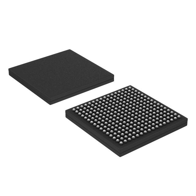


 工商网监
湘ICP备2023018690号
工商网监
湘ICP备2023018690号
