NJW4830
Single High Side Switch
GENERAL DESCRIPTION
PACKAGE OUTLINE
The NJW4830 is the single high-side switch that can supply
0.5A.
The active clamp circuit, overcurrent and thermal shutdown are
built-in with Pch MOS FET.
It can be controlled by a logic signal (3V/5V) directly. Therefore, it
is suitable for Car accessory, Industrial Equipments and other
applications.
NJW4830U2
FEATURES
Drain-Source Voltage
45V
Drain Current
0.5A
Corresponding with Logic Voltage Operation: 3V/5V
Low On-Resistance
0.35Ω (typ.)
Low Consumption Current
110µA (typ.)
Active Clamp Circuit
Over Current Protection
Thermal Shutdown
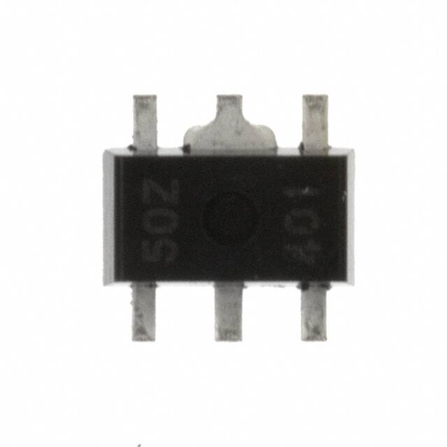
Package Outline
SOT89-5
PIN CONFIGURATION
5
2
4
1
2
3
1. IN
2. GND
3. FLT
4. VDD
5. OUT
BLOCK DIAGRAM
VDD
FLT
Over
Current
Protection
FLT
DELAY
VDD
Level Shift
IN
Thermal
Shut Down
GND
Ver.2014-01-08
Active
Clamp
OUT
-1-
�NJW4830
ABSOLUTE MAXIMUM RATINGS
PARAMETER
SYNBOL
Drain-Source Voltage
VDS
Supply Voltage
VDD
Input Voltage
VIN
FLT Pin Voltage
VFLT
Power Dissipation
PD
RATINGS
+45
+45
−0.3 to +6
−0.3 to +6
625 (*1)
2,400 (*2)
UNIT
V
V
V
V
mW
(Ta=25°C)
REMARK
VDD–OUT Pin
VDD–GND Pin
IN–GND Pin
FLT–GND Pin
–
Active Clamp Tolerance
EAS
10
mJ
–
(Single Pulse)
Active Clamp Current
IAP
0.5
A
–
Junction Temperature
Tj
–
−40 to +150
°C
Operating Temperature
Topr
–
−40 to +85
°C
Storage Temperature
Tstg
–
−50 to +150
°C
(*1): Mounted on glass epoxy board. (76.2×114.3×1.6mm:based on EIA/JDEC standard size, 2Layers, Cu area 100mm2)
(*2): Mounted on glass epoxy board. (76.2×114.3×1.6mm:based on EIA/JDEC standard, 4Layers)
(For 4Layers: Applying 74.2×74.2mm inner Cu area and a thermal via hall to a board based on JEDEC standard JESD51-5)
RECOMMENDED OPERATING CONDITIONS
PARAMETER
SYMBOL
MIN.
Drain–Source Voltage
VDS
0
Supply Voltage
VDD
4.6
Output Current
IO
0
Input Pin Voltage
VIN
0
FLT Pin Voltage
VFLT
0
-2-
TYP.
–
–
–
–
–
MAX.
40
40
0.5
5.5
5.5
UNIT
V
V
A
V
V
REMARK
VDD–OUT Pin
VDD–GND Pin
VDD–OUT Pin
IN–GND Pin
FLT–GND Pin
Ver.2014-01-08
�NJW4830
ELECTRICAL CHARACTERISTICS
PARAMETER
(Unless otherwise noted, VDS=13V, Ta=25°C)
SYMBOL
Drain-Source Output Clamp Voltage
VDSS_CL
VIH
VIL
CONDITIONS
VIN=0V, IO=1mA, VDD=40V
IO=10mA
IO=100µA
MIN.
TYP.
MAX.
UNIT
VDD-45
2.64
–
–
–
–
–
–
0.9
V
V
V
2.64
–
5.5
V
High Level Input Voltage
Low Level Input Voltage
Protection Circuit Function
Input Voltage Range
OUT Pin Leak Current
at OFF State
Quiescent Current 1
Quiescent Current 2
Input Current
On-state Resistance
IOLEAKOUT
VIN=0V, VDD=40V
–
–
1
µA
IDD1
IDD2
IIN
RDS_ON
VIN=0V, VDD=40V
VIN=5V
VIN=5V
VIN=5V, IO=0.5A
–
–
–
–
–
110
150
0.35
1
150
190
0.6
µA
µA
µA
Ω
Over Current Protection1
ILIMIT1
VIN=5V, VDS=5V
0.5
0.75
1.2
A
Over Current Protection2
Turn-on Time
Turn-off Time
OUT–VDD Voltage Difference
FLT Pin Low Level
Output Voltage
FLT Pin Leak Current
at High Level
FLT Delay Time
ILIMIT2
tON
tOFF
VPDOV
VIN=5V, VDD=VDS=40V
VIN=0 to 5V, IO=0.5A
VIN=5 to 0V, IO=0.5A
VIN=0V, IORH=1A
0.1
–
–
–
0.4
20
20
0.85
–
–
–
1.2
A
µs
µs
V
VVFLT
IFLT=500µA
–
0.25
0.5
V
IOLEAKFLT
VFLT=5.5V
–
–
1
µA
VIN=0 to 5V, VDS=22V
–
5
–
ms
VIN_opr
TRUTH TABLE
Input Signal
Operating Condition
tDFLT
FLT Pin
Output Status
L
H
Normal
H
L
OFF
ON
L
H
Over Current ILIMIT1
H
L
OFF
ILIMIT1
L
H
Over Current ILIMIT2
H
L
OFF
ILIMIT2
L
H
Tj >150°C
H
H
OFF
OFF
Ver.2014-01-08
-3-
�NJW4830
TIMING CHRAT
ON, OFF Switching Time (VIN=0 to 5V, VDD=13V, IO=0.5A)
90%
IN
10%
90%
OUT
10%
tON
tOFF
FLT Delay Time (VIN=0 to 5V, VDD=VDS=22V)
IN
50%
90%
FLT
tDFLT
FLT Delay Time Measurement Circuit
+
V
5V
NJW4830
VDS
VDD
5V
0V
IN
OUT
FLT GND
-4-
Ver.2014-01-08
�NJW4830
High
Input signal
Low
ON
Over Current
Protection
OFF
ON
Thermal Protection
OFF
VDD
Output voltage
VDSS_CL
0V
ILIMIT1
Inductive
load
ILIMIT2
Output current
0A
tDFLT
High
Fault signal
Low
Normal
Ver.2014-01-08
Current limit1
Current limit2
Thermal
shutdown
Active clamp
-5-
�NJW4830
OVER CURRENT PROTECTION CHARACTERISTIC
IO [A]
ILIMIT1
ILIMIT2
VDS [V]
L
FLT Terminal
H
TYPICAL APPLICATION
+
V
Logic Voltage
ex. 5V, 3V
NJW4830
VDD
Micro
Controller
Drive Signal
IN
FAULT
-6-
FLT GND
OUT
RL
Ver.2014-01-08
�NJW4830
CHARACTERISTICS
Drain-Source Clamp Voltage
vs.Ambient Temperature
1
63
0.9
61
0.8
Quiescent Current2 [mA]
Drain-Source Clamp Voltage [V]
65
59
57
55
53
51
49
47
Quiescent Current2 vs.Ambient Temperature
0.7
0.6
0.5
0.4
0.3
0.2
0.1
45
0
-50
-25
0
25 50 75 100 125 150
Ambient Temperature [ºC]
-50
Input Current vs. Input Voltage
0.5
-25
0
25 50 75 100 125 150
Ambient Temperature [ºC]
Input Current vs.Ambient Temperature
1
0.9
0.8
Input Current [mA]
Input Current [mA]
0.4
0.3
0.2
0.1
0.7
0.6
0.5
0.4
0.3
0.2
0.1
0
0
0
Ver.2014-01-08
1
2
3
4
Input Voltage [V]
5
6
-50
-25
0
25 50 75 100 125 150
Ambient Temperature [ºC]
-7-
�NJW4830
CHARACTERISTICS
ON-state Resistance
vs. Supply Voltage
0.6
0.6
0.5
ON-state Resistance [Ω]
ON-state Resistance [Ω]
0.5
0.4
0.3
0.2
0.1
0.4
0.3
0.2
0.1
0
0
0
5
10
15 20 25 30
Supply Voltage [V]
35
40
-50
Over Current Protection1 vs. Ambient Temperature
1.2
-25
0
25 50 75 100 125 150
Ambient Temperature [ºC]
Over Current Protection2 vs. Ambient Temperature
1.2
1
Over Current Limit2 [A]
1
Over Current Limit1 [A]
ON-state Resistance vs. Ambient Temperature
0.8
0.6
0.4
0.2
0.8
0.6
0.4
0.2
0
0
-50
-25
0
25 50 75 100 125 150
Ambient Temperature [ºC]
-50
-25
0
25 50 75 100 125 150
Ambient Temperature [ºC]
Output Current vs.Drain-Source Voltage
1.2
Output Current [A]
1
0.8
0.6
0.4
0.2
0
0
-8-
5
10 15 20 25
30
Drain-Source Voltage [V]
35
40
Ver.2014-01-08
�NJW4830
CHARACTERISTICS
Turn-on Time vs. Ambient Temperature
30
25
Turn-off Time [µs]
Turn-on Time [µs]
25
20
15
10
20
15
10
5
5
0
0
-50
-25
0
25 50 75 100 125 150
Ambient Temperature [ºC]
-50
FLT Pin Low Level
Output Voltage vs.
Ambient Temperature
0.3
7
FLT Delay Time [ms]
FLT Pin Low Level
Output Voltage [V]
-25
0
25 50 75 100 125 150
Ambient Temperature [ºC]
FLT Delay Time vs. Ambient Temperature
6
0.25
0.2
0.15
0.1
0.05
5
4
3
2
1
0
0
-50
TSD Detect / Release Temperature [ºC]
Turn-off Time vs. Ambient Temperature
30
-25
0
25 50 75 100 125 150
Ambient Temperature [ºC]
-50
-25
0
25 50 75 100 125 150
Ambient Temperature [ºC]
TSD Detect / Release Temperature vs. Input Voltage
180
Detection Temperature
170
160
150
Release Temperature
140
130
120
0
Ver.2014-01-08
1
2
3
4
Input Voltage [V]
5
6
-9-
�Application Tips
NJW4830
Technical Information
Regarding Active Clamp Capacity of High/Low side Switch Products
What is “Active Clamp Capacity”.
The IC might suffer to damage by the inductive kickback at the transient time of ON state to OFF state, when an
inductive load such as a solenoid or motor is used for the load of the high-side/low-side switch.
The protection circuit for the inductive kickback is the active clamp circuit. The energy that can be tolerated by the
active clamp circuit is called "Active Clamp Capacity (EAS)".
When using an inductive load to the high-side/low-side switch, you should design so that the ESW does not exceed the
active clamp capability.
IC operation without an external protection parts (Fig 1)
Active Clamp
Current IAP
tA
ID
Active Clamp Period
VDS
Active Clamp
Current IAP
ID
VDD
0V
Time
Drain-Source Clamp Voltage
V DSS_CL
Drain-Source Clamp Voltage
V DSS_CL
VDS
VDD
0V
VIN
Time
5V
VIN
0V
tA Active Clamp Period
5V
0V
tON
tON
Fig1. Active Clamp Waveform (Left: Low-side Switch / Light High-side Switch)
At when the VIN turns off, the drain-source voltage (VDS) increases rapidly by the behavior of the inductive load that is
keeping current flowing. However, it will be clamped at VDSS_CL by the active clamp circuit. At the same time, the drain
current is flowed by adjusting the gate voltage of the output transistor, and the energy is dissipated at the output transistor.
The energy: ESW is shown by the following formula.
tA
E SW = ∫ VDS (t ) ⋅ I D (t )dt =
0
VDSS _ CL
1
2
LI AP ⋅
2
VDSS _ CL − VDD
The ESW is consumed inside IC as heat energy. However, the thermal shutdown does not work when the VIN is 0V.
Therefore in worst case the IC might break down. When using the active clamp, you should design ESW does not
exceed the EAS.
- 10 -
Ver.2014-01-08
�Application
Tips
NJW4830
Technical Information
Application Hint
The simplest protection example is to add an external flywheel diode at the load to protect IC from an inductive
kickback. (Fig.2)
Flywheeling Diode
ID
VDD
VDD
VIN
DRAIN
SOURCE
VDD
OUT
VIN
V DS
V DS
ID
GND
Flywheeling Diode
Fig 2. Application Circuit of Inductance Load Driving (Left: Low-side Switch / Light High-side Switch)
[CAUTION]
The specifications on this databook are only
given for information , without any guarantee
as regards either mistakes or omissions. The
application circuits in this databook are
described only to show representative usages
of the product and not intended for the
guarantee or permission of any right including the
industrial rights.
Ver.2014-01-08
- 11 -
�
很抱歉,暂时无法提供与“NJW4830U2-TE2”相匹配的价格&库存,您可以联系我们找货
免费人工找货