NJW4187
High Voltage Io=1000mA Low Dropout Regulator
GENERAL DESCRIPTION
The NJW4187 is a high voltage and low current consumption low
dropout regulator.
It has two lineups as A version (built-in ON/OFF function type) and
B version (3-terminal / compatible with 78 series)
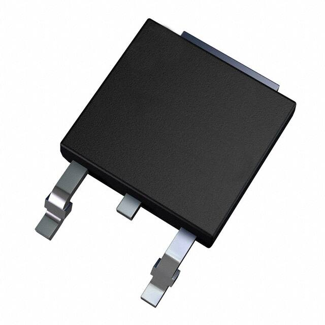
PACKAGE OUTLINE
NJW4187 is mounted to TO-252-3/-5 packages and corresponded to
Low ESR capacitor (MLCC).
The wide input range makes NJW4187 suitable for a Car accessory,
industrial supplies, battery equipment and various applications.
FEATURES
Wide Operating Voltage Range
Low Current Consumption
NJW4187DL3
NJW4187DL1
4.0V to 40V
55μA typ. (A version)
48μA typ. (B version)
VO 1.0%
IO (min.)=1000mA
2.0V to 15V
High Precision Output
Output Current
Output Voltage Range
Correspond to Low ESR capacitor (MLCC)
ON/OFF Control (apply only the A version)
Internal Thermal Overload Protection
Internal Over Current Protection
Package Outline
A ver. TO-252-5
B ver. TO-252-3
PRODUCT CLASSIFICATION
Device Name
Version
NJW4187DL3-xxA
A
NJW4187DL1-xxB
B
xx=Output Voltage ex) 33=3.3V 05=5.0V
ON/OFF
Function
Yes
-
Package
TO-252-5
TO-252-3
PIN CONFIGURATION
4
VOUT
NC
3
GND
2
CONTROL
VIN
5
3
1
NJW4187DL3-A
Ver.2016-02-15
2
3
VOUT
2
GND
1
VIN
NJW4187DL1-B
-1-
�NJW4187
BLOCK DIAGRAM
・A version
VOUT
VIN
Current
Limit
CONTROL
Bandgap
Reference
Thermal
Protection
GND
・B version
VIN
VOUT
Current
Limit
Bandgap
Reference
Thermal
Protection
GND
OUTPUT VOLTAGE RANK LIST
・A version
Device Name
Output Voltage
NJW4187DL3-33A
3.3V
NJW4187DL3-05A
5.0V
・B version
Device Name
NJW4187DL1-33B
NJW4187DL1-05B
-2-
Output Voltage
3.3V
5.0V
Ver.2016-02-15
�NJW4187
ABSOLUTE MAXIMUM RATINGS
PARAMETER
SYNBOL
Input Voltage
VIN
Control Voltage(*1)
VCONT
Output Voltage
VOUT
Power Dissipation
Junction Temperature
Operating Temperature
Storage Temperature
PD
Tj
Topr
Tstg
RATINGS
-0.3 to +45
-0.3 to +45
-0.3 to VIN 17
1190 (*2)
3125 (*3)
-40 to +150
-40 to +125
-40 to +150
(Ta=25 C)
UNIT
V
V
V
mW
C
C
C
(*1): Apply only the A version.
2
(*2): Mounted on glass epoxy board. (76.2 114.3 1.6mm:based on EIA/JDEC standard size, 2Layers, Cu area 100mm )
(*3): Mounted on glass epoxy board. (76.2 114.3 1.6mm:based on EIA/JDEC standard, 4Layers)
(For 4Layers: Applying 74.2 x 74.2mm inner Cu area and thermal via hole to a board based on JEDEC standard JESD51-5)
INPUT VOLTAGE RANGE
VIN=4.0V to 40V
ELECTRICAL CHARACTERISTICS
Unless otherwise noted, VIN =VO+1V, CIN=1.0μF, CO=4.7μF(3V VO 3.4V: CO=10μF), Ta=25°C
PARAMETER
SYMBOL
TEST CONDITION
MIN.
TYP.
MAX.
UNIT
Output Voltage
VO
IO =200mA
-1.0%
+1.0%
V
55
90
A version, IO =0mA, except ICONT
μA
Quiescent Current
IQ
B version, IO =0mA
48
83
Quiescent Current
at Control OFF (*4)
IQ (OFF)
VCONT=0V
-
-
1
μA
Output Current
Line Regulation
Load Regulation
IO
VO/ VIN
VO/ IO
VO 0.9
1000
-
0.03
0.004
0.42
mA
%/V
%/mA
Ripple Rejection
Dropout Voltage (*5)
Average Temperature
Coefficient of Output Voltage
Control Current (*4)
Control Voltage
for ON-state (*4)
Control Voltage
for OFF-state (*4)
IO=600mA
-
58
54
0.27
VO/ Ta
Ta=0 to 85 C, IO =200mA
-
50
-
ppm/ C
ICONT
VCONT=1.6V
-
1
3
μA
VCONT(ON)
1.6
-
-
V
VCONT(OFF)
-
-
0.6
V
RR
VIO
VIN = VO+1V to 40V, IO=200mA
IO=0mA to 1000mA
VIN = VO+1V ,ein=200mVrms,
f=1kHz, IO =10mA
VO=3.3V
VO=5.0V
dB
V
(*4): Apply only the A version.
(*5): The output voltage excludes under 3.8V
The above specification is a common specification for all output voltages.
Therefore, it may be different from the individual specification for a specific output voltage.
* These parameters are tested by Pulse Measurement.
Ver.2016-02-15
-3-
�NJW4187
THERMAL CHARACTERISTICS
PARAMETER
SYMBOL
Junction-to-Ambient
ja
thermal resistance
Junction-to-Top of package
jt
characterization parameter
VALUE
105 (*6)
40 (*7)
17 (*6)
12 (*7)
UNIT
C/W
C/W
2
(*6): Mounted on glass epoxy board. (76.2 114.3 1.6mm:based on EIA/JDEC standard size, 2Layers, Cu area 100mm )
(*7): Mounted on glass epoxy board. (76.2 114.3 1.6mm:based on EIA/JDEC standard, 4Layers)
(For 4Layers: Applying 74.2 74.2mm inner Cu area and a thermal via hole to a board based on JEDEC standard JESD51-5)
POWER DISSIPATION vs. AMBIENT TEMPERATURE
NJW4187DL1/DL3 PowerDissipation
(Topr=-40~+125°C,Tj=150°C)
3500
Power Dissipation PD(mW)
3000
on 4 layers board
2500
2000
on 2 layers board
1500
1000
500
0
-50
-25
0
25
50
75
100
125
150
Temperature : Ta( C)
-4-
Ver.2016-02-15
�NJW4187
TEST CIRCUIT
・A version
A
IIN
VIN
VOUT
*8
VIN
1.0μF
A
ICONT
NJW4187-A
4.7μF
IOUT V VOUT
(Ceramic)
*8 : Vo
很抱歉,暂时无法提供与“NJW4187DL1-33B-TE1”相匹配的价格&库存,您可以联系我们找货
免费人工找货