TS78M00 Series
Taiwan Semiconductor
3-Terminal 500mA Positive Voltage Regulator
FEATURES
The TS78M00 Series positive voltage regulators are
●
Output Voltage Range 5V & 12V
identical to the popular TS7800 Series devices, except
●
Output current up to 500mA
that they are specified for only half the output current.
●
No external components required
Like the TS7800 devices, the TS78M00 Series 3-
●
Internal thermal overload protection
Terminal regulators are intended for local, on-card
●
Internal short-circuit current limiting
voltage regulation. Internal current limiting, thermal
●
●
●
Output transistor safe-area compensation
Output voltage offered in 4% tolerance
Compliant to RoHS Directive 2011/65/EU and
WEEE 2002/96/EC
Halogen-free according to IEC 61249-2-21
shutdown circuitry and safe-area compensation for the
internal pass transistor combine to make these devices
en
de
d
DESCRIPTION
remarkably rugged under most operating conditions.
Maximum output current with adequate heatsink is
500mA
●
APPLICATION
Switching power supply
●
Home appliance
mm
●
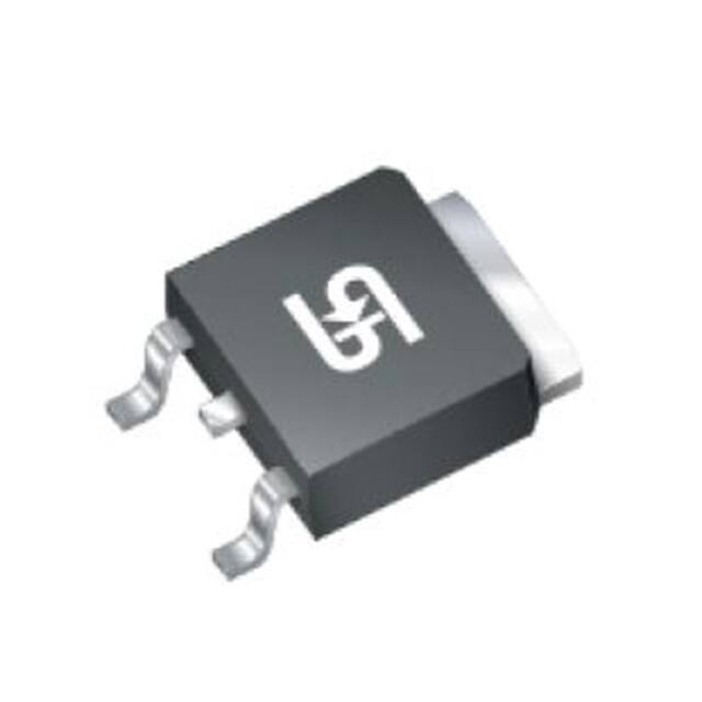
Pin Definition:
1. Input
2. Ground (Tab)
3. Output
eco
TO-252 (DPAK)
tR
Notes: MSL 3 (Moisture Sensitivity Level) per J-STD-020
No
TYPICAL APPLICATION CIRCUIT
A common ground is required between the input and the output voltages. The input voltage must remain typically 2.0V above
the output voltage even during the low point on the Input ripple voltage.
XX = these two digits of the type number indicate voltage.
* = Cin is required if regulator is located an appreciable distance from power supply filter.
** = Co is not needed for stability; however, it does improve transient response.
1
Version: F1512
�TS78M00 Series
Taiwan Semiconductor
ABSOLUTE MAXIMUM RATINGS
PARAMETER
SYMBOL
LIMIT
UNIT
DC Input Voltage
VIN
35
V
Power Dissipation
PD
Internally Limited
W
Operating Junction Temperature Range
TJ
0 ~ +150
o
TSTG
-65~+150
o
SYMBOL
LIMIT
Storage Temperature Range
C
C
THERMAL PERFORMANCE
RӨJC
Junction to Ambient Thermal Resistance
RӨJA
10
°C/W
100
°C/W
de
Junction to Case Thermal Resistance
UNIT
d
PARAMETER
Notes: RӨJA is the sum of the junction-to-case and case-to-ambient thermal resistances. The case thermal reference is defined
at the solder mounting surface of the drain pins. RӨJA is guaranteed by design while RӨCA is determined by the user’s board
en
design. RӨJA shown below for single device operation on FR-4 PCB in still air.
ELECTRICAL SPECIFICATIONS TS78M05
o
o
PARAMETER
mm
(VIN=10V, IOUT=350mA, 0 C≤TJ≤125 C, CIN=0.33µF, COUT=0.1µF, unless otherwise noted)
SYMBOL
CONDITION
MIN
TYP
MAX
4.80
5
5.20
4.75
5
5.25
--
3
100
--
1
50
5mA≤IOUT≤500mA
--
15
100
5mA≤IOUT≤200mA
--
5
50
IOUT=0, TJ=25°C
--
3
6
7.5V≤VIN≤25V
--
--
0.8
5mA≤IOUT≤350mA
--
--
0.5
TJ=25°C
Line Regulation
7.5V≤VIN≤20V
5mA≤IOUT≤350mA
7.5V≤VIN≤25V
TJ=25°C
8V≤VIN≤12V
REGLINE
REGLOAD
TJ=25°C
tR
Load Regulation
VOUT
e co
Output voltage
Quiescent Current
Quiescent Current Change
IQ
ΔIQ
UNIT
V
mV
mA
VN
10Hz≤f≤100KHz, TJ=25°C
--
40
--
µV
Ripple Rejection Ratio
RR
f=120Hz, 8V≤VIN≤18V
62
78
--
dB
VDROP
IOUT=500mA, TJ=25°C
--
2
--
V
ROUT
f=1kHz
--
17
--
mΩ
IOS
TJ=25°C
--
50
--
mA
IO peak
TJ=25°C
--
0.7
--
A
IOUT= 5mA, 0°C≤TJ≤125°C
--
-0.2
--
mV/°C
No
Output Noise Voltage
Voltage Drop
Output Resistance
Output Short Circuit
Current
Peak Output Current
Temperature Coefficient of
Output Voltage
ΔVOUT/ΔTJ
Note:
1. Pulse testing techniques are used to maintain the junction temperature as close to the ambient temperature as possible,
and thermal effects must be taken into account separately
2. This specification applies only for DC power dissipation permitted by absolute maximum ratings.
2
Version: F1512
�TS78M00 Series
Taiwan Semiconductor
ELECTRICAL SPECIFICATIONS TS78M05
o
o
(VIN=19V, IOUT=350mA, 0 C≤TJ≤125 C, CIN=0.33µF, COUT=0.1µF, unless otherwise noted)
SYMBOL
CONDITION
TJ=25°C
Output voltage
VOUT
Line Regulation
REGLINE
REGLOAD
Quiescent Current
IQ
Quiescent Current Change
TJ=25°C
MAX
11.53
12
12.48
11.42
12
12.60
--
10
240
--
3
120
--
12
240
5mA≤IOUT≤500mA
5mA≤IOUT≤200mA
IOUT=0, TJ=25°C
14.5V≤VIN≤27V
ΔIQ
TYP
--
4
120
--
3
6
--
--
0.8
--
--
0.5
de
Load Regulation
14.5V≤VIN≤27V
5mA≤IOUT≤350mA
14.5V≤VIN≤30V
TJ=25°C
15V≤VIN≤19V
MIN
5mA≤IOUT≤350mA
UNIT
V
mV
d
PARAMETER
mA
VN
10Hz≤f≤100KHz, TJ=25°C
--
75
--
µV
Ripple Rejection Ratio
RR
f=120Hz, 15V≤VIN≤25V
--
80
--
dB
VDROP
IOUT=500mA, TJ=25°C
--
2
--
V
f=1kHz
--
18
--
mΩ
TJ=25°C
--
50
--
mA
TJ=25°C
--
0.7
--
A
IOUT= 5mA, 0°C≤TJ≤125°C
--
-0.3
--
mV/°C
Output Resistance
ROUT
Output Short Circuit
Current
Peak Output Current
IOS
IO peak
ΔVOUT/ΔTJ
e co
Temperature Coefficient of
Output Voltage
mm
Voltage Drop
en
Output Noise Voltage
tR
Note:
1. Pulse testing techniques are used to maintain the junction temperature as close to the ambient temperature as possible,
and thermal effects must be taken into account separately
2. This specification applies only for DC power dissipation permitted by absolute maximum ratings.
No
ORDERING INFORMATION
OUTPYT VOLTAGE
PART NO.
PACKAGE
PACKING
5V
TS78M05CP ROG
TO-252 (DPAK)
2,500pcs / 13" Reel
12V
TS78M12CP ROG
TO-252 (DPAK)
2,500pcs / 13" Reel
3
Version: F1512
�TS78M00 Series
Taiwan Semiconductor
de
d
ELECTRICAL CHARACTERISTIC CURVE
Figure 2. Dropout Voltage vs.
Junction Temperature
e co
mm
en
Figure 1. Bias Current vs. Input Voltage
Figure 4. Ripple Rejection vs. Frequency
No
tR
Figure 3. Bias Current vs. Output Current
Figure 6. Peak Output Current vs. Dropout
Voltage
4
Version: F1512
�TS78M00 Series
Taiwan Semiconductor
PACKAGE OUTLINE DIMENSIONS (Unit: Millimeters)
tR
e co
mm
SUGGESTED PAD LAYOUT (Unit: Millimeters)
en
de
d
TO-252 (DPAK)
MARKING DIAGRAM
= Output Voltage
05 =5V
12 =12V
= Year Code
= Month Code for Halogen Free Product
O =Jan P =Feb Q =Mar R =Apr
S =May T =Jun U =Jul
V =Aug
W =Sep X =Oct
Y =Nov Z =Dec
= Lot Code
No
XX
Y
M
L
5
Version: F1512
�TS78M00 Series
No
tR
e co
mm
en
de
d
Taiwan Semiconductor
Notice
Specifications of the products displayed herein are subject to change without notice. TSC or anyone on its behalf,
assumes no responsibility or liability for any errors or inaccuracies.
Information contained herein is intended to provide a product description only. No license, express or implied, to
any intellectual property rights is granted by this document. Except as provided in TSC’s terms and conditions of
sale for such products, TSC assumes no liability whatsoever, and disclaims any express or implied warranty,
relating to sale and/or use of TSC products including liability or warranties relating to fitness for a particular purpose,
merchantability, or infringement of any patent, copyright, or other intellectual property right.
The products shown herein are not designed for use in medical, life-saving, or life-sustaining applications.
Customers using or selling these products for use in such applications do so at their own risk and agree to fully
indemnify TSC for any damages resulting from such improper use or sale.
6
Version: F1512
�
很抱歉,暂时无法提供与“TS78M05CP ROG”相匹配的价格&库存,您可以联系我们找货
免费人工找货