1cell Li-ion/Li-polymer battery protection IC
MM3825 series
Outline
The MM3825 series are protection IC using high voltage CMOS process for overcharge, overdischarge and
overcurrent protection of the rechargeable Lithium-ion or Lithium-polymer battery. The overcharge, overdischarge,
discharging overcurrent, charging overcurrent, and short protection of the rechargeable one-cell Lithium-ion or
Lithium-polymer battery can be detected. Each of these IC composed of four voltage detectors, short detection
circuit, reference voltage sources, oscillator, counter circuit and logical circuits.
Features
・Detection voltage
(Unless otherwise specified, Ta=25 degC)
Range
Accuracy
Overcharge detection voltage
3.6V to 5.0V, 5mV steps
+/-20mV
Overdischarge detection voltage
2.0V to 3.0V, 50mV steps
+/-35mV
Discharging overcurrent detection voltage
20mV to +300mV, 1mV steps
+/-2.5mV
Charging overcurrent detection voltage
-20mV to -300mV, 1mV steps
+/-2.5mV
Short detection voltage
70mV to 350mV, 1mV steps
+/-8%
+/-25mV(Ta=-20 to +60 degC)
+/-3.0mV(Ta=-20 to +60 degC)
+/-3.0mV(Ta=-20 to +60 degC)
0V battery charge inhibition battery voltage 1.1V to 2.4V, 0.1V steps
0.9V
・0V battery charge function
+/-0.1V
+/-0.3V
Selectable "Permission" or "inhibition"
・Current consumption at Ta=25 degC
Normal mode
2.5uA typ. 4.0uA max.
Standby mode
0.1uA max. (Overdischarge latch function enable.)
0.5uA max. (Overdischarge latch function disable.)
MM3825Txx Series
Normal mode
2.0uA typ. 3.0uA max.
Standby mode
0.05uA max. (Overdischarge latch function enable.)
0.5uA max. (Overdischarge latch function disable.)
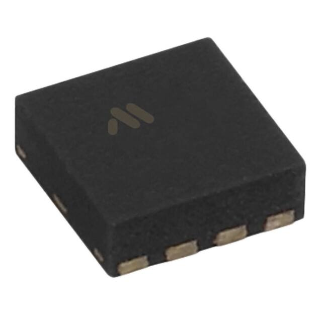
Package type
・SSON-6J/6M
1.40 × 1.40 × 0.55 [mm]
・SON-6C
2.00 × 1.60 × 0.55 [mm]
■ All brand names, logos, product names, trade names and service names described here are trademarks or registered trademarks of their respective companies or organizations.
■ Any products mentioned in this leaflet are subject to any modification in their appearance and others for improvements without prior notification.
■ The details listed here are not a guarantee of the individual products at the time of ordering. When using the products, you will be asked to check their specifications.
Oct, 2020 Rev.0
�Block Diagram
Package and pin configuration
SSON-6J/6M
Function
Pin No. Symbol
1
1
6
2
5
3
4
2
3
SON-6C
No connection
NC
COUT Charge FET control terminal
DOUT Discharge FET control terminal
4
VSS
Negative power supply voltage input terminal
5
VDD
Positive power supply voltage input terminal
6
V-
Negative power supply voltage input terminal.
Function
Pin No. Symbol
1
1
6
2
5
3
4
2
3
NC
No connection
COUT Charge FET control terminal
DOUT Discharge FET control terminal
4
VSS
Negative power supply voltage input terminal
5
VDD
Positive power supply voltage input terminal
6
V-
Negative power supply voltage input terminal.
Oct, 2020 Rev.0
�Package dimensions
Unit:mm
SON-6C
SSON-6J
SSON-6M
Top View
Top View
Top View
Bottom View
Bottom View
Bottom View
Marking Contents / S0N-6C
Marking Contents / SSON-6J
Marking Contents / SSON-6M
← Model No.
← Date Code
← Date Code
← Date Code
← Model No.
← Model No.
1-Pin Mark
1-Pin Mark
Oct, 2020 Rev.0
�Absolute Maximum Ratings
Parameter
Supply voltage
V-
Rating
Symbol
Unit
VDD
-0.3 to 12
V
V-
VDD-28 to VDD+0.3
V
COUT terminal
terminal
VCOUT
VDD-28 to VDD+0.3
V
DOUTterminal
VDOUT
VSS-0.3 to VDD+0.3
V
Tstg
-55 to +125
degC
Storage temperature
Recommended Operating Conditions
Parameter
Symbol
Rating
Operating ambient temperature
Topr
-40 to +85
Unit
degC
Operating voltage
Vop
1.5 to 5.5
V
Electrical characteristics
Item
Operating voltage
Operating Ambient temperature
Note
(Unless otherwise specified, Ta=25 degC)
Min
Typ
Max
Unit
Symbol
V
Vop
1.5
-
5.5
degC
Ta
-40
-
85
Rshort*0.6
Rshort
Rshort*2.0
Rpu*0.5
Rpu
Rpu*2.0
0.5
Discharge overcurrent release resistance
kohms
V- terminal pull-up resistances
kohms
Rshort VDD=3.6V, V-=2.0V
Rpu
VDD=2.0V, V-=0V
COUT L level output voltage
V
VcoL
Icout=30uA, VDD=4.5V
-
0.1
COUT H level output voltage
V
VcoH
Icout=-30uA, VDD=4.0V
VDD-0.5
VDD-0.1
-
DOUT L level output voltage
V
VdoL
Idout=30uA, VDD=2.0V
-
0.1
0.5
Idout=-30uA, VDD=4.0V
DOUT H level output voltage
V
VdoH
Current consumption
uA
Idd
Current consumption at stand-by
uA
Is
VDD-0.5
VDD-0.1
-
VDD=4.0V, V-=0V
-
2.5
4
VDD=2.0V *3
-
-
0.1
VDD=2.0V *4
-
0.3
0.5
Vst=VDD-V-, VDD=0V *1
-
-
1.2
Vst=VDD-VSS, V-=0V *2
Vst-0.1
0V battery charge permission charger voltage
V
0V battery charge inhibition battery voltage
V
Overcharge detection voltage
V
Overcharge release voltage
V
Vrel1
Overdischarge detection voltage
V
Vdet2 V-=0V
Vst
Vst
Vst+0.1
Vdet1
Vde1+0.020
Vrel1-0.030
Vrel1
Vrel1+0.030
Vdet1-0.035
Vdet2
Vdet1 Ta=-20 to 60degC, V-=0V Vdet1-0.020
*5
In case Vdet2=Vrel2 *3 *5
Vrel2-0.035
In case Vdet2≠Vrel2 *4 *5
Vdet1-0.065
Vrel2
Vde1+0.035
Vrel2+0.050
Overdischarge release voltage
V
Vrel2
Discharging overcurrent detection voltage
V
Vdet3 VDD=3.6V, V-=0V *6
Vdet3-⊿V
Vdet3
Vdet3+⊿V
Charging overcurrent detection voltage
V
Vdet4 VDD=3.6V, V-=0V *6
Vdet4-⊿V
Vdet4
Vdet4+⊿V
Vdet1+0.090
Vshort*0.92
Vshort
Vshort*1.08
Overcharge detection delay time
ms
tVdet1
tVdet1*0.8
tVdet1
tVdet1*1.2
Short detection voltage
V
Vshort VDD=3.6V
Overdischarge detection delay time
ms
tVdet2
tVdet2*0.8
tVdet2
tVdet2*1.2
Discharging overcurrent detection delay time
ms
tVdet3
tVdet3*0.8
tVdet3
tVdet3*1.2
Charging overcurrent detection delay time
ms
tVdet4
tVdet4*0.8
tVdet4
tVdet4*1.2
Short detection delay time
us
tVshort
tVshort*0.7
tVshort
tVshort*1.4
*1 In case 0V battery charge function "Permission".
*4 Overdischarge mode latch function "Disable".
*2 In case 0V battery charge function "inhibition".
*5 Please refer to each specifications for release condition.
*3 Overdischarge mode latch function "Enable".
*6 Current detection voltage Accuracy
Oct, 2020 Rev.0
�Typical application circuit
Symbol
Part
Min.
Typ.
Max.
R1
Resistor
-
100Ω
1.0kΩ For voltage fluctuation, For ESD
Purpose
C1
Capacitor
0.01uF
0.1uF
1.0uF
R2
Resistor
-
1.0kΩ
1.0kΩ Current limit for charger reverse connection
C2
Capacitor
-
0.1uF
-
For exogenous noise
C3
Capacitor
-
0.1uF
-
For exogenous noise
Nch MOS FET
-
-
-
Charge and discharge control
DFET
CFET
For voltage fluctuation
Application hints
R1 and C1 stabilize a supply voltage fluctuation. However, the detection voltage rises by the current consumption of
IC when R1 is too large, and please use 1kohm or less for R1. Please use 0.01uF or more for C1 to stabilize the
operation.
Oct, 2020 Rev.0
�Overcharge release voltage
Overdischarge detection voltage
Overdischarge release voltage
Discharging overcurrent detection
voltage
Charging overcurrent detection
voltage
Short detection voltage1
Overdischarge
Hys-Cancel
Overcharge
Discharge overcurrent
Overdischarge
PKG
Overcharge
MODEL
0V charge
Protection mode latch
function
Overcharge detection voltage
Lineup
Vdet1
[V]
Vrel1
[V]
Vdet2
[V]
Vrel2
[V]
Vdet3
[mV]
Vdet4
[mV]
Vshort
[mV]
MM3825ACCYLE
SON-6C
0.9
Disable Disable Disable Enable Disable 4.475
4.275
2.500
2.900
20.0
-20.0
70.0
MM3825CM1RRE
SSON-6J
1.1
Disable Enable Disable Enable Enable 4.275
4.175
2.400
2.400
90.0
-25.0
250.0
MM3825CM3YRE
SON-6C
0.9
Disable Enable Disable Enable Enable 4.475
4.275
2.700
2.700
45.0
-45.0
145.0
Permission Disable Enable Disable Enable Enable 4.475
MM3825CN3YRE
SON-6C
4.275
2.500
2.500
30.0
-30.0
105.0
MM3825TM3YRE
SON-6C
0.9
Disable Disable Disable Enable Disable 4.475
4.275
2.500
2.800
60.0
-60.0
190.0
MM3825TM4RRE
SSON-6J
2.1
Disable Enable Disable Enable Enable 4.200
4.000
2.800
2.800
50.0
-50.0
150.0
MM3825TN1YRE
SON-6C
Permission Disable Enable Disable Enable Enable 4.495
4.295
2.500
2.500
45.0
-45.0
150.0
Delay time
MODEL
tVdet1 [s]
tVrel1 [ms]
tVdet2 [ms]
tVrel2 [ms]
tVdet3 [ms]
tVrel3 [ms]
tVdet4 [ms]
tVrel4 [ms]
tshort [us]
MM3825ACCYLE
1.024
16.00
64.00
1.00
16.00
1.00
16.00
1.00
280
MM3825CM1RRE
1.024
16.00
32.00
1.00
24.00
1.00
8.00
1.00
250
MM3825CM3YRE
1.024
16.00
32.00
1.00
16.00
1.00
8.00
1.00
280
MM3825CN3YRE
1.024
16.00
32.00
1.00
8.00
1.00
8.00
1.00
280
MM3825TM3YRE
1.024
16.00
20.00
1.00
12.00
1.00
8.00
1.00
280
MM3825TM4RRE
1.024
8.00
128.00
1.00
8.00
1.00
8.00
1.00
280
MM3825TN1YRE
1.024
16.00
32.00
1.00
32.00
1.00
8.00
1.00
280
Oct, 2020 Rev.0
�
很抱歉,暂时无法提供与“MM3855AJ1RRE”相匹配的价格&库存,您可以联系我们找货
免费人工找货