FT 3120® and FT 3150® Free
Topology Smart Transceivers
Features
• Combines an ANSI/CEA 709.3-1999 compliant free topology twisted pair
transceiver with a Neuron 3120 or Neuron 3150 network processor core
• Supports polarity insensitive free topology star, daisy chain, bus, loop, or
mixed topology wiring
• 78 kilobits per second bit rate for distances up to 500 meters
in free topology or 2700 meters in bus topology with double terminations
• High performance Neuron network processor core enables concurrent processing of application code and network
packets (40MHz maximum for FT 3120 smart transceiver, 20MHz maximum
for FT 3150 smart transceiver)
FT 3120 transceiver in a 44-pin TQFP
package[1]
• 4Kbytes of embedded EEPROM for application code and configuration data
on the FT 3120 smart transceiver and 0.5Kbytes of embedded EEPROM for
configuration data on the FT 3150 smart transceiver
• Interface for external memory for devices with larger memory requirements
(FT 3150 smart transceiver only)
• 2Kbytes of embedded RAM for buffering network data and network variables
• 11 I/O pins with 34 programmable standard I/O modes minimizing external interface circuitry
• Unique 48-bit Neuron ID in every device for network installation and management
• Compact external transformer with patent pending
architecture providing exceptional immunity from magnetic interference and
high frequency common mode noise
• Compatible with TP/FT-10 channels using FTT-10 and/or FTT-10A Free Topology Transceivers and, with suitable DC blocking capacitors, LPT-10 Link
Power Transceivers
• Communications parameters preprogrammed for the TP/FT-10 channel at
10MHz
• 5V operation with low power consumption
• -40 to +85°C operating temperature range[3, 4
www.echelon.com
�Description
The FT 3120 and FT 3150 Free Topology
Smart Transceivers
integrate a Neuron® 3120 or Neuron 3150
network processor core, respectively, with a
free topology twisted pair transceiver to
create a low cost, smart transceiver on a
chip. Combined with Echelon's high performance FT-X1 or FT-X2 Communication
Transformer, the FT 3120 and FT 3150
smart transceivers set new benchmarks for
performance, robustness, and low cost.
Ideal for use in LonWorks® devices destined
for building, industrial, transportation,
home, and utility automation applications,
the FT 3120 and FT 3150 Free Topology
Smart Transceivers can be used in both
new product designs and as a means of
cost reducing existing nodes.
The integral transceiver is fully compatible
with the TP/FT-10 channel and can communicate with devices using Echelon's
FTT-10A Free Topology Transceiver, and,
when used with suitable DC isolation capacitors, the LPT-11 Link Power Transceiver.
The free topology transceiver supports polarity insensitive cabling using a star, bus,
daisy-chain, loop, or combination topology
(see Figure 1)—freeing the installer from the
need to adhere to a strict set of wiring
rules. Free topology wiring reduces the
time and expense of node installation by allowing the wiring to be installed in the
most expeditious and cost-effective manner. It also simplifies network expansion by
eliminating restrictions on wire routing,
splicing, and node placement.
The FT 3120 Free Topology Smart Transceiver is a complete system-on-a-chip that
is targeted at cost-sensitive and small form
factor designs with a need for up to
4Kbytes of application code. The Neuron
3120 core operates at up to 40MHz[2], and
includes 4Kbytes of EEPROM and 2Kbytes
of RAM. The Neuron firmware is pre-programmed in an on-chip ROM. The application code is stored in the embedded
EEPROM memory and may be updated
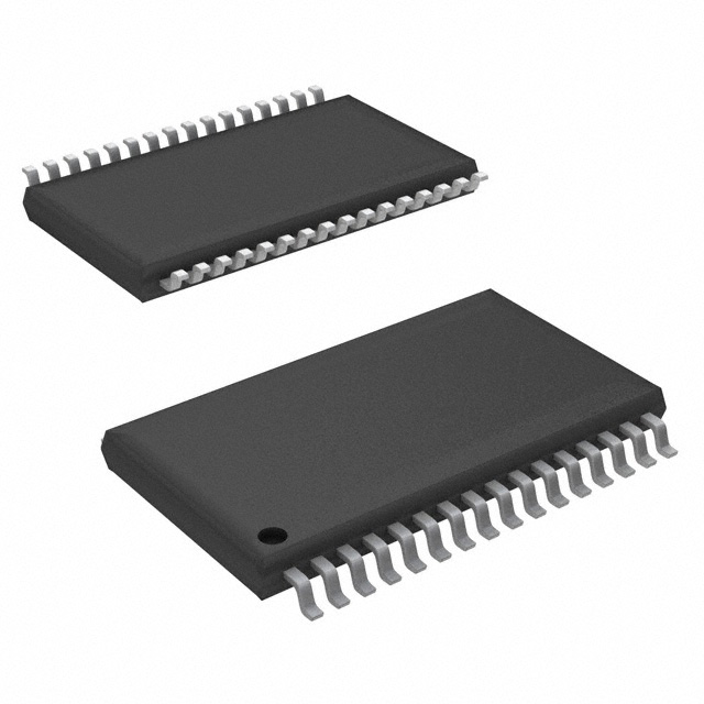
over the network. The FT 3120 smart transceiver is offered in a 32-lead SOIC package
as well as a compact 44-lead TQFP package.
FT 3150 smart transceiver can address up
to 58Kbytes of external memory, of which
16Kbytes of external nonvolatile memory is
dedicated to the Neuron firmware. The FT
3150 transceiver is supplied in a 64-lead
TQFP package.
input/output modes. Combining a wide
range of I/O models with two on-board
timer/counters enable the FT 3120 and FT
3150 smart transceivers to interface to application circuits with minimal external logic
or software development.
The embedded EEPROM may be written
up to 10,000 times with no data loss. Data
stored in the EEPROM will be retained for
at least 10 years.[3]
Easy Interface to Any
Host MCU
Three different versions of the FT 3120 and
FT 3150 Free Topology Smart Transceivers
are available to meet a wide range of applications and packaging requirements. See
FT 3120 and FT 3150 Free Topology Smart
Transceiver Ordering Information below for
product offerings and descriptions.
The FT-X1 is a through-hole communication
transformer while the FT-X2 is a surface
mount transformer. Either transformer can
be used with the FT 3120 or FT 3150 Free
Topology Smart Transceivers. the FT-X1 and
FT-X2 transformers have similar noise immunity and performance characteristics.
Models 14212R-500, 14222R-800, 14230R450, 14240R, and 14250R-300 are compliant with the European Directive
2002/95/EC on the restriction of the use of
certain hazardous substances (RoHS) in
electrical and electronic equipment.
Flexible I/O, Simple
Configuration
The FT 3120 and FT 3150 Free Topology
Smart Transceivers provide 11 I/O pins
which may be configured to operate in one
or more of 34 predefined standard
The FT 3120 and FT 3150 Free Topology
Smart Transceivers can be easily interfaced
to other host MCUs via Echelon’s ShortStack® or MIP firmware. When used with
the ShortStack or MIP firmware, the Smart
Transceiver enables any OEM product with
a host microcontroller to quickly and inexpensively become a networked, Internetaccessible device. The ShortStack firmware
uses an SCI or SPI serial interface to communicate between the host and the Smart
Transceiver. The MIP uses a high performance parallel or dual-ported RAM interface.
Advanced Network Noise
Protection
The FT 3120 and FT 3150 Free Topology
Smart Transceivers are composed of two
components — the FT 3120/FT 3150 IC and
an external communication transformer.
The transformer enables operation in the
presence of high frequency common mode
noise on unshielded twisted pair networks.
Properly designed nodes can meet the rigorous Level 3 requirements of EN 61000-46 without the need for a network isolation
choke. The transformer also offers outstanding immunity from magnetic noise,
eliminating the need for protective mag-
The FT 3150 Free Topology Smart Transceiver includes a 20MHz Neuron 3150 core,
0.5Kbytes of EEPROM, and 2Kbytes of
RAM. Through its external memory bus, the
Figure 1. Typical Free Topologies Supported by the FT 3120 and FT 3150
Free Topology Smart Transceivers
Notes:
1 See table on FT 3120 and FT 3150 Free Topology Smart Transceiver Ordering Information for other product offerings and description.
2 The FT 3120 Free Topology Smart Transceiver is designed to run at frequencies up to 40MHz using an external clock oscillator. External oscillators may
take several milliseconds to stabilize after power-up. The FT 3120 Free Topology Smart Transceiver operating at 40MHz should be held in reset until the
CLK1 input is stable. With some oscillators, this may require the use of a power-on-reset-pulse stretching Low-Voltage Detection chip/circuit. Check the
oscillator specifications for more information on startup stabilization times.
3 EEPROM programming must be limited to -25 to 85°C for a 10-year data retention over the -40 to 85°C operating temperature range.
4 Maximum junction temperature should not exceed 105ºC. Tjunction can be calculated as follows: Tjunction = TAmbient + V•I•θJA where θJA for 32-pin
SOIC = 51°C/W, θJA for 44-pin TQFP = 43°C/W, and θJA for 64-pin TQFP = 44°C/W.
www.echelon.com
�netic shields in most applications. The
transformer is provided in a potted, 6-pin,
through-hole plastic package.
FT-X1/FT-X2 Communication Transformers
must be ordered separately. See FT 3120
and FT 3150 Free Topology Smart Transceiver Ordering Information for product offerings and descriptions. The FT 3120 / FT
3150 Free Topology Smart Transceiver IC
and the FT-X1/FT-X2 Communication Transformer are designed to be used as a pair
and therefore must be implemented together in all designs. No transformer other
than the FT-X1 or FT-X2 Communication
Transformer may be used with either the
FT 3120 or FT 3150 Free Topology Smart
Transceiver IC, or the smart transceiver
warranty will be void.
A typical FT 3120 or FT 3150 based device
requires a power source, crystal and an I/O
interface to the device being controlled
(see Figure 3 for a typical FT 3120 / FT
3150 based device).
Figure 2. Upgrading to an FT 3120-E4S40 IC and FT-X1 Communication Transformer from a 32-pin SOIC Neuron
3120 Chip and FTT-10A
Notes:
5 Certain devices providing Rx packet detection LEDs may not be pin compatible with the FT 3120 and FT 3150 Free Topology Smart Transceiver.
Contact Echelon for details.
6 The FT-X1/FT-X2 Communication Transformer must be ordered separately and must be used with the FT 3120 / FT 3150 Free Topology Smart
Transceiver IC in all designs.
www.echelon.com
�Figure 3. Typical FT 3120 / FT 3150 Free Topology Smart Transceiver based Node
Figure 4. FT 3120 / FT 3150 Free Topology Smart Transceiver Block Diagram
www.echelon.com
�Figure 5. FT 3120 / FT 3150 Free Topology Smart Transceiver IC Pin Configurations
Figure 5a.
Figure 5b.
Figure 5c.
Notes:
7 The small dimple at the bottom left of the marking indicates pin 1.
8 NC (No Connect) — Should not be used. (These pins are reserved for internal testing.)
www.echelon.com
�FT 3120 / FT 3150 Free Topology Smart Transceiver IC Pin Descriptions
Pin Name
Type
CLK1
Input
CLK2
Output
RESET
SERVICE
IO0-IO3
IO4-IO7
IO8-IO10
D0-D7
Pin Functions
Oscillator connection or external clock
input.
Oscillator connection. Leave open when external
clock is input to CLK1. Maximum of one external
HCMOS equivalent load.
Reset pin (active LOW).
Note: The allowable external capacitance
connected to the RESET pin is 100pF-1000pF.
Service pin (active LOW). Alternates between
input and output at a 76Hz rate.
I/O
(Built-in
Pull-up)
I/O
(Built-in
Configurable
Pull-up)
I/O
Large current-sink capacity (20mA). General I/O
port. The output of timer/counter 1 may be routed
to IO0. The output of timer/counter 2 may be routed
to IO1.
I/O
General I/O port. The input of timer/counter 1 may
(Built-in
be derived from one of IO4-IO7. The input to
Configurable timer/counter 2 may be derived from IO4.
Pull-up)
I/O
General I/O port. May be used for serial
communication under firmware control.
I/O
Bi-directional memory data bus.
FT 3150-P20
TQFP-64
Pin Number
24
FT 3120-E4S40
SOIC-32
Pin Number
15
23
FT 3120-E4P40
TQFP-44
Pin Number
15
14
14
6
1
40
17
8
5
2, 3, 4, 5
7, 6, 5, 4
4, 3, 2, 43
10, 11, 12, 13
3, 30, 29, 28
42, 36, 35, 32
14, 15, 16
27, 26, 24
31, 30, 27
43, 42, 38, 37,
36, 35, 34, 33
45
46
47, 50, 51, 52,
53, 54, 55, 56,
57, 58, 59, 60
61, 62, 63, 64
7, 20, 22, 26,
40, 41, 44
8, 19, 21, 25, 39
N/A
N/A
N/A
N/A
N/A
N/A
N/A
N/A
R/W
E
A0-A15
Output
Output
Output
Read/write control output for external memory.
Enable clock control output for external memory.
Memory address output port.
VDD
Power
VSS
Power
ICTMode
Input
Power input (5V nom). All VDD pins must be
2, 11, 12,
9, 10, 19,
connected together externally.
18, 25, 32
29, 38, 41
Power input (0V, GND). All VSS pins must be
9, 13, 16, 23, 31
7, 13, 16, 26, 37
connected together externally.
In-circuit test mode control. Driving the ICTMode
high and RESET low will put the device in the
In-Circuit Test mode (all pins are placed in a
high impedance state).
9
10
8
Analog pin to be interfaced with T1 of the
28
19
20
external transformer. Corresponds to CP0 on
Toshiba and Cypress Neuron Chips.
Analog pin to be interfaced with T2 of the
29
20
21
external transformer. Corresponds to CP1 on
Toshiba and Cypress Neuron Chips.
May be used to monitor, transmit/receive
30
17
18
activity. Driven high during data transmissions,
driven low when receiving data and kept at high
impedance otherwise.
SLEEP. May be configured as an output to
31
21
24
indicate when the FT 3120 / FT 3150 is in sleep
mode. Corresponds to CP3 on Toshiba and
Cypress Neuron Chips.
Reserved for future use. Must be pulled up to 5V.
32
22
25
Corresponds to CP4 on Toshiba and Cypress
Neuron Chips.
No connect. Must be left open.
1, 18, 27, 48, 49
N/A
1, 6, 11, 12, 17,
22, 23, 28, 33,
34, 39, 44
T1
I/O
T2
I/O
COMM_ACTIVE
Output
SLEEP
Output
RTMP
Input
NC
—
www.echelon.com
�FT-X1 Communication Transformer Pin Configuration
FT-X2 Communication Transformer Pin Configuration
FT-X1/FT-X2 Communication Transformer Pin Descriptions
Pin Name
Pin Function
NET_B
Network Port, polarity Insensitive
Transformer
Pin Number
1
NET_A
Network Port, polarity Insensitive
2
T1
Internally connects to pin 5. Alternate connection to T1 pin on the FT 3120 /
FT 3150 IC. Corresponds to the RXD pin on the FTT-10A (for replacement
with FT-X1).
3
(Not used on
FT-X2)
T2
Internally connects to pin 6. Alternate connection to T2 pin on the FT 3120 /
FT 3150 IC. Corresponds to the TXD pin on the FTT-10A (for replacement
with FT-X1).
4
(Not used on
FT-X2)
T1
Connects to the ESD/transient protection circuitry and T1 pin on the FT 3120
/ FT 3150 IC. Internally connects to pin 3 of the FT-X1. Corresponds to the T1
pin on the FTT-10A (for replacement with FT-X1).
5
T2
Connects to the ESD/transient protection circuitry and T2 pin on the FT 3120
/ FT 3150 IC. Internally connects to pin 4 of the FT-X1. Corresponds to the T2
pin on the FTT-10A (for replacement with FT-X1).
6
www.echelon.com
�Electrical Characteristics (VDD = 4.75-5.25V)
Parameter
Description
Min.
Input
Low
Voltage
VIL
IO0-IO10, SERVICE, D0-D7, RESET
VIH
Input High Voltage
IO0-IO10, SERVICE, D0-D7, RESET
2.0
VOL
Low-Level Output Voltage
Iout < 20μA
Standard Outputs (IOL = 1.4 mA)[9]
High Sink (IO0-IO3), SERVICE, RESET (IOL = 20 mA)
High Sink (IO0-IO3), SERVICE, RESET (IOL = 10 mA)
Maximum Sink (COMM_ACTIVE) (IOL = 40 mA)
Maximum Sink (COMM_ACTIVE) (IOL = 15 mA)
VOH
High-Level Output Voltage
Iout < 20μA
VDD - 0.1
VDD - 0.4
Standard Outputs (IOH = -1.4 mA)[9]
VDD - 0.4
High Sink (IO0-IO3), SERVICE (IOH = -1.4 mA)
V
DD - 1.0
Maximum Sink (COMM_ACTIVE) (IOL = -40 mA)
VDD - 0.4
Maximum Sink (COMM_ACTIVE) (IOL = -15 mA)
Vhys
Hysteresis (Excluding CLK1)
175
Iin
Input Current (Excluding Pull-ups) (VSS to VDD)[10]
Ipu
Pull-up Source Current (Vout = 0 V, Output = High-Z)[10]
60
[11, 12]
IDD
Operating Mode Supply Current
40MHz Clock
IDD(receive)
IDD(transmit)
20MHz Clock
IDD(receive)
IDD(transmit)
10MHz Clock
IDD(receive)
IDD(transmit)
5MHz Clock
IDD(receive)
IDD(transmit)
Max.
Unit
V
0.8
V
V
0.1
0.4
0.8
0.4
1.0
0.4
V
+/- 10
260
60
75
42
57
35
50
20
35
mV
μA
μA
mA
mA
mA
mA
mA
mA
mA
mA
LVI Trip Point (VDD)
Part Number
FT 3120 and FT 3150
Min.
3.8
Typ.
4.1
Max.
4.4
Unit
V
www.echelon.com
�External Memory Interface Timing — FT 3150
(VDD = 4.75 to 5.25 V, TA = -40 to +85 C)[3]
See Figures 7 through 12 for detailed measurement information)
Parameter
tcyc
PWEH
Description
Memory Cycle Time (System Clock Period)
Pulse Width, E High [13]
CL
PWEL
Pulse Width, E Low
tAD
Delay, E High to Address Valid
tAH
tRD
Address Hold Time After E High
Delay, E High to R/W Valid Read
tRH
tWR
R/W Hold Time Read After E High
Delay, E High to R/W Valid Write
tWH
tDSR
R/W Hold Time Write After E High
Read Data Setup Time to E High
tDHR
tDHW
tDDW
Data Hold Time Read After E High
Data Hold Time Write After E High [14]
Delay, E Low to Data Valid
tacc[15]
External Read Access Time (tacc = tcyc - tAD - tDSR) at 20MHz Input Clock
30ρF
50ρF
≥30ρF
30ρF
50ρF
≥30ρF
30ρF
50ρF
≥30ρF
30ρF
50ρF
≥30ρF
≥30ρF
30ρF
50ρF
30ρF
tacc[15]
External Read Access Time (tacc = tcyc - tAD - tDSR) at 10MHz Input Clock
50ρF
Min.
100
tcyc/2 - 5
Max.
400
tcyc/2 + 5
tcyc/2 - 5
tcyc/2 + 5
ns
35
45
ns
10
25
45
Unit
ns
ns
ns
ns
5
25
45
5
15
25
0
10
ns
ns
12
60
50
ns
130
ns
ns
Notes:
9 Standard outputs are IO4-IO10. (RESET is an open drain input/output. CLK2 must have 15pF load.) For FT 3150, standard outputs also include
A0-A15, D0-D7, E, and R/W.
10 IO4-IO7 and SERVICE have configurable pull-ups. RESET has a permanent pull-up.
11 Supply current measurement conditions: all outputs under no-load conditions, all inputs 0.2V or (VDD - 0.2V), configurable pull-ups off and
crystal oscillator clock input disabled.
12 Maximum supply current values are at midpoint of supply voltage range.
13 tcyc = 2/f where f is the input clock (CLK1) frequency (20, 10, or 5 MHz).
14 The data hold parameter, tDHW, is measured to disable levels shown in Figure 12, rather than to the traditional data invalid levels.
15 This parameter considers only the memory read access time from address to data. This does not allow for chip enable decode. A more thorough analysis should be performed for any given design.
External Memory Interface Timing Diagram
Figure 7
www.echelon.com
�Figure 8
Signal Loading for Timing Specifications
Figure 9
Test Point Levels for E Pulse Width Measurements
Figure 10
Drive Levels and Test Point Levels for Timing Specifications
Unless Otherwise Specified
Figure 11
Test Point Levels for High Impedence-to-Driven Time Measurements
Figure 12
Test Point Levels for Driven-to High Impedence Time Measurements
www.echelon.com
�Recommended FT 3120 / FT 3150 Free Topology Smart Transceiver IC Pad Layouts
Figure 13a
Figure 13b
Figure 13c
Recommended FT-X2 Pad Layout (4 pins)
Figure 14
www.echelon.com
�FT 3120 / FT 3150 Free Topology Smart Transceiver IC Package Diagrams
Figure 15a
Figure 15b
www.echelon.com
�FT-X1 Communication Transformer
Top View
FT-X1 Communication
Transformer Side View
(Dimensions in mm)
(Dimensions in mm)
Figure 16a
Figure 16b
www.echelon.com
�FT-X2 Communication Transformer SMT Package Diagram
Figure 17
General Specifications
Data Communications Type
Network Polarity
Isolation Between Network and
0-60Hz, 60 seconds
0-60Hz, continuous
EMI
ESD
Radiated Electromagnetic Susceptibility
Fast Transient/Burst Immunity
Surge Immunity
Conducted RF Immunity
Safety Approvals (FT-X1/FT-X2 Communication Transformer)
Transmission Speed
Number of Transceivers Per Segment
Network Wiring
Network Length in Free Topology
[17]
Network Length in Doubly Terminated
Bus Topology
[17]
Differential Manchester coding
Polarity insensitive
1000Vrms
277Vrms
Designed to comply with FCC Part 15 Level B and EN55022 Level B
Designed to comply with EN 61000-4-2, Level 4
Designed to comply with EN 61000-4-3, Level 3
Designed to comply with EN 61000-4-4, Level 4
Designed to comply with EN 61000-4-5, Level 3
Designed to comply with EN 61000-4-6, Level 3
Recognized by UL to Standards UL 60950, 2000 and CSA C22.2 No. 60950,
2000
Recognized by TÜV EN 60950
78 kilobits per second
Up to 64
24 to 16AWG twisted pair; see User’s Guide or Junction Box and Wiring
Guidelines application note for qualified cable types
1000m (3,280 feet) maximum total wire with one repeater
500m (1,640 feet) maximum total wire with no repeaters
500m (1,640 feet) maximum device-to-device distance
[16]
5400m (17,710 feet) with one repeater
2700m (8,850 feet) with no repeaters
www.echelon.com
�General Specifications (continued)
Maximum Stub Length in Doubly-Terminated
Bus Topology
Network Termination
Power-down Network Protection
Physical Layer Repeater
Operating Temperature
Operating Humidity
Non-operating Humidity
Vibration
Mechanical Shock
Reflow Soldering Temperature Profile
Peak Reflow Soldering Temperature
3m (9.8 feet)
One terminator in free topology; two terminators in bus topology
(see FT 3120 / FT 3150 Free Topology Smart Transceiver Data Book)
High impedance when unpowered
The FT 3120/FT 3150 Free Topology Smart Transceiver cannot be used to
implement a physical layer repeater. In the event that the limits on the number
of transceivers or total wire distance are exceeded, FTT-10A transceivers may be
used to create physical layer repeaters. See FTT-10A Free Topology Transceiver
User’s Guide for more details.
-40 to 85°C
25-90% RH @50°C, non-condensing
95% RH @ 50°C, non-condensing
1.5g peak-to-peak, 8Hz-2kHz
100g (peak)
Refer to Joint Industry Standard document IPC/JEDEC J-STD-020C (July 2004)
220ºC (Models 14210-500 and 14211-500)
235ºC (Models 14220-800, 14221-800, and 14230-450)
245ºC (Model 14212R-500)
260ºC (Models 14222R-800 and 14230R-450)
245ºC (FT-X2 Model 14250R-300)
[3]
Ordering Information
(Note: The FT 3120/FT 3150 Free Topology Smart Transceiver IC and the FT-X1/FT-X2 Communication Transformer must be ordered in the same quantities.)
The following tables lists the non-RoHS compliant Free Topology Smart Transceivers. These products will be discontinued after Q4 2005.
Free Topology Smart
Transceiver IC
Product Number
Model
Number
Firmware
Version
Maximum
Input
Clock
EEPROM
RAM
ROM
External
Memory Interface
IC
Package
(Factory Default OnChip) Data Comm Parameters
FT 3120-E4S40
14210-500
v13
40MHz
4K Bytes
2K Bytes
12K Bytes
No
32 SOIC
TP/XF-1250
FT 3120-E4S40
14211-500
v13
40MHz
4K Bytes
2K Bytes
12K Bytes
No
32 SOIC
TP/FT-10 @ 10MHz
FT 3120-E4P40
14220-800
v13
40MHz
4K Bytes
2K Bytes
12K Bytes
No
44 TQFP
TP/XF-1250
FT 3120-E4P40
14221-800
v13
40MHz
4K Bytes
2K Bytes
12K Bytes
No
44 TQFP
TP/FT-10 @ 10MHz
FT 3150-P20
14230-450
N/A
20MHz
0.5K Bytes
2K Bytes
N/A
Yes
64 TQFP
N/A
Free Topology Smart
Transceiver IC
Product Number
Model
Number
Firmware
Version
Maximum
Input
Clock
EEPROM
RAM
ROM
External
Memory Interface
IC
Package
(Factory Default OnChip) Data Comm Parameters
FT 3120-E4S40
14212R-500
v16
40MHz
4K Bytes
2K Bytes
12K Bytes
No
32 SOIC
TP/FT-10 @ 10MHz
FT 3120-E4P40
14222R-800
v16
40MHz
4K Bytes
2K Bytes
12K Bytes
No
44 TQFP
TP/FT-10 @ 10MHz
FT 3150-P20
14230R-450
N/A
20MHz
0.5K Bytes
2K Bytes
N/A
Yes
64 TQFP
N/A
Notes:
16 Safety agency hazardous voltage barrier requirements are not supported.
17 Network segment length varies depending on wire type. See Junction Box and Wiring Guidelines application note for detailed specifications.
www.echelon.com
�Free Topology Smart Transceiver Product Number Description
Communication Transformer
Product Number
Model Number
Transformer Package
RoHS Compliant
FT-X1
14240
6-pin through-hole
No
FT-X1
14240R
6-pin through-hole
Yes
FT-X2
14250R-300
4-pin surface-mount
Yes
Documentation
The FT 3120 / FT 3150 Free Topology Smart Transceiver Data Book may be downloaded from Echelon’s web site, or ordered
through Echelon’s literature fulfillment department.
Product
FT 3120 / FT 3150 Free Topology Smart Transceiver Data Book
Echelon Part Number
005-0139-01
Copyright © 2000-2014, Echelon Corporation. Echelon, LON, LonWorks, LonMark, LonBuilder, NodeBuilder, LonManager, LonTalk, LonUsers, LonPoint, Digital Home, Neuron, 3120, 3150, LNS,
i.LON, LonWorld, ShortStack, Panoramix, LonMaker, the Echelon logo, and the LonUsers logo are trademarks of Echelon Corporation registered in the United States and other countries. LonLink,
LonResponse, LonSupport, LONews, Open Systems Alliance, OpenLDV, Powered by Echelon, LNS Powered by Echelon, Panoramix Powered by Echelon, LonWorks Powered by Echelon, Networked Energy Services Powered by Echelon, NES Powered by Echelon, Digital Home Powered by Echelon, Pyxos, and Thinking Inside the Box are trademarks of Echelon Corporation. Other
trademarks belong to their respective holders.
Disclaimer
Neuron Chips, Smart Transceivers, and other OEM Products were not designed for use in equipment or systems which involve danger to human health or safety or a risk of property damage and
Echelon assumes no responsibility or liability for use of the Neuron Chips or Free Topology Twisted Pair Transceiver Modules in such applications. ECHELON MAKES AND YOU RECEIVE NO
WARRANTIES OR CONDITIONS, EXPRESS, IMPLIED, STATUTORY OR IN ANY COMMUNICATION WITH YOU, AND ECHELON SPECIFICALLY DISCLAIMS ANY IMPLIED WARRANTY OF MERCHANTABILITY OR FITNESS FOR A PARTICULAR PURPOSE.
003-0337-01H
www.echelon.com
�