NJM17431
ADJUSTABLE PRECISION SHUNT REGULATOR
■FEATURES
■GENERAL DESCRIPTION
Operating Voltage
Precision Voltage Reference
VREF to 36V
2.495V 0.8
2.5V 0.8
Adjustable Output Voltage by external resistance
Wide Safety Operating Boundary Area
Bipolar Technology
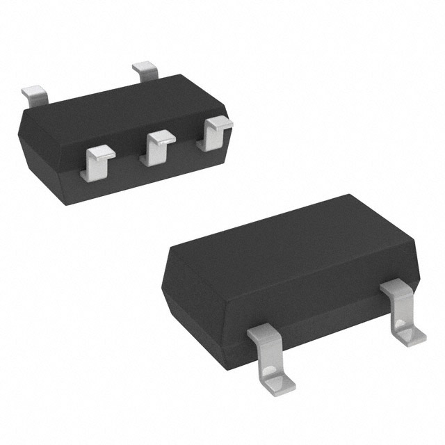
Package
SOT-23-5
SOT-89-3
■APPLICATION
The NJM17431 is adjustable precision shunt
regulator. The output voltage may be set to any value
between VREF (about 2.5V) and 36V by two external
resistors.
The NJM17431 is improved the reference voltage
accuracy ( 0.8) and safety operating boundary area
connected large capacitance. Therefore, the
NJM17431 is suitable for various applications.
Industrial Equipment
Home Electrical Appliance
Replacement from Zener Diode
Other
■BLOCK DIAGRAM
CATHODE
CATHODE
REFERENCE
+
REFERENCE
V REF
ANODE
Ver.1.2
http://www.njr.com/
ANODE
-1-
�NJM17431
■PIN CONFIGURATION
4
5
1
Pin Assign
2
1
3
2
3
1. REFERENCE
1. REFERENCE
2. ANODE
2. ANODE
3. CATHODE
3. CATHODE
4. N.C.
5. N.C.
Package
SOT-89-3
SOT-23-5
Product
Number
NJM17431Uxx
NJM17431FxxA
■PRODUCT NAME INFORMATION
NJM17431 - U/F - 24/25 - A - (TE1)
Part
Number
Package
VREF
U: SOT-89-3
F: SOT-23-5
24: 2.495V
25: 2.5V
Pin assign
Taping Form
Option
■ORDERING INFORMATION
MARKING
WEIGHT
(mg)
MOQ
(pcs)
181
61
1,000
Sn2Bi
171
61
1,000
15
3,000
15
3,000
HALOGEN- TERMINAL
FREE
FINISH
PRODUCT NAME
PACKAGE
RoHS
NJM17431U24
SOT-89-3
Yes
Yes
Sn2Bi
NJM17431U25
SOT-89-3
Yes
Yes
NJM17431F24A
SOT-23-5
Yes
Yes
Sn2Bi
AK5x
(“x” is Lot)
NJM17431F25A
SOT-23-5
Yes
Yes
Sn2Bi
AK4x
(“x” is Lot)
Ver.1.2
http://www.njr.com/
-2-
�NJM17431
■ABSOLUTE MAXIMUM RATINGS
PARAMETER
SYMBOL
MAXIMUM
RATINGS
UNIT
REMARK
VKA
37 (1)
V
ANODE-CATHODE Pin
IK
100 to 150
mA
ANODE-CATHODE Pin
IREF
0.05 to 10
480 (2)
650 (3)
mA
–
mW
–
Cathode Voltage
Continuous Cathode Voltage
Reference Input Current
SOT-23-5
Power Dissipation
PD
450 (4)
1300 (5)
SOT-89-3
Junction Temperature
Tjmax
150
C
–
Operating Temperature Range
Topr
40 to 125
C
–
Storage Temperature Range
Tstg
50 to 150
C
–
(1) Unless specified, all voltage value are with respect to the anode pin.
(2) Mounted on glass epoxy board. (76.2×114.3×1.6mm: based on EIA/JEDEC standard, 2Layers)
(3) Mounted on glass epoxy board. (76.2×114.3×1.6mm: based on EIA/JEDEC standard, 4Layers),
internal Cu area: 74.2×74.2mm
(4) Mounted on glass epoxy board. (76.2×114.3×1.6mm: based on EIA/JEDEC standard size, 2Layers)
(5) Mounted on glass epoxy board. (76.2×114.3×1.6mm: based on EIA/JEDEC standard, 4Layers)
(For 4Layers: Applying 74.2×74.2mm inner Cu area and a thermal via hole to a board based on JEDEC standard
JESD51-5)
■RECOMMENDED OPERATING CONDITIONS
PARAMETER
SYMBOL
RATINGS
Cathode Voltage
VKA
VREF to 36
V
ANODE-CATHODE Pin
Cathode Current
IK
0.5 to 100
mA
ANODE-CATHODE Pin
Ver.1.2
http://www.njr.com/
UNIT
REMARK
-3-
�NJM17431
■ELECTRICAL CHARACTERISTICS
PARAMETER
(Unless other noted, IK=10mA、Ta=25C)
SYMBOL
Reference Voltage
VREF
TEST CONDITIONS
VKA= VREF (6)
MIN.
TYP.
MAX.
2.495V ver.
2.475
2.495
2.515
2.5V ver.
2.480
2.500
2.520
UNIT
V
Reference Input Voltage
Change Over Temperature
Range
∆VREF
(dev)
VKA=VREF (6)
Ta= - 40˚C to +85˚C
-
8
17
mV
Reference voltage
temperature coefficient
∆VREF
(ppm)
VKA=VREF (6)
Ta= - 40˚C to +85˚C
-
30
-
ppm/C
Reference Voltage Change
vs. Cathode Voltage Change
∆VREF/
∆VKA
∆VKA=10V-VREF (7)
∆VKA=36V-10V
-
-2.0
-1
-3.7
-2.2
mV/V
IREF
R1=10kΩ, R2=∞ (7)
-
1
2.8
µA
Reference Input Current
Change Over Temperature
Range
∆IREF
(dev)
R1=10kΩ, R2=∞ (7)
Ta= - 40˚C to +85˚C
-
0.25
0.5
µA
Minimum Cathode Current
IMIN
VKA=VREF (6)
-
0.25
0.5
mA
OFF State Cathode Current
IOFF
-
0.1
1.0
µA
Dynamic Impedance
ΙZKAΙ
VKA=36V, VREF=0V (8)
VKA=VREF, IK=1mA to 100mA,
f≤1kHz (6)
-
0.2
0.5
Ω
Reference Input Current
The maximum value of “Dynamic Impedance“, “Reference Voltage Change” and “Reference Input Current Change” are
determined based on sampling evaluation from the initial production lots, and thus not tested in the production test.
Therefore, these values are for the reference design purpose only.
(6): TestCircuitFig.1
(7): Test CircuitFig.2
(8): Test Circuit Fig.3
■ TEST CIRCUIT
INPUT
VKA
INPUT
VKA
IK
IK
R1
VREF
Fig.1. Test Circuit for VKA=VREF
VO=VKA=VREF
Ver.1.2
R2
INPUT
VKA
IOFF
IREF
VREF
Fig.2. Test Circuit for VKA >VREF
Fig.3. Test Circuit for IOFF
R1
VO V KA V REF 1
IREF R1
R2
http://www.njr.com/
-4-
�NJM17431
■THERMAL CHARACTERISTICS
PARAMETER
SYMBOL
Junction-to-ambient
thermal resistance
VALUE
SOT-23-5
260 (2)
195 (3)
SOT-89-3
200 (4)
130 (5)
SOT-23-5
60 (2)
70 (3)
SOT-89-3
67 (4)
65 (5)
θja
Junction-to-Top of package
characterization parameter
UNIT
ψjt
°C /W
°C /W
(2) Mounted on glass epoxy board. (76.2×114.3×1.6mm: based on EIA/JEDEC standard, 2Layers)
(3) Mounted on glass epoxy board. (76.2×114.3×1.6mm: based on EIA/JEDEC standard, 4Layers),
internal Cu area: 74.2×74.2mm
(4) Mounted on glass epoxy board. (76.2×114.3×1.6mm: based on EIA/JEDEC standard size, 2Layers)
(5) Mounted on glass epoxy board. (76.2×114.3×1.6mm: based on EIA/JEDEC standard, 4Layers)
(For 4Layers: Applying 74.2×74.2mm inner Cu area and a thermal via hole to a board based on JEDEC standard
JESD51-5)
■POWER DISSIPATION vs. AMBIENT TEMPERATURE
NJM17431F
Power Dissipation
NJM17431U
Power Dissipation
(Topr=-40ºC to +125ºC, Tj=150ºC)
(Topr=-40ºC to +125ºC, Tj=150ºC)
1600
800
700
1400
(3) on 4 Layers Board
1200
Package Power : Pd [mW]
600
Package Power : Pd [mW]
(5) on 4 Layers Board
(2) on 2 Layers Board
500
400
300
1000
800
600
(4) on 2 Layers Board
200
400
100
200
0
0
-50
-25
0
25
50
75
100
125
150
-50
-25
Ambient Temperature : Ta [ºC]
Ver.1.2
http://www.njr.com/
0
25
50
75
100
125
150
Ambient Temperature : Ta [ºC]
-5-
�NJM17431
■TYPICAL CHARACTERISTICS
Reference Voltage vs. Cathode Current
Reference Voltage vs. Temperature
VKA=VREF, Ta=25°C
2.55
2.54
2.54
Reference Voltage:VREF [V]
Reference Voltage:VREF [V]
VKA=VREF, IK=10mA
2.55
2.53
2.52
2.51
2.50
2.49
2.48
2.47
2.53
2.52
2.51
2.50
2.49
2.48
2.47
2.46
2.46
2.45
2.45
0.1
1
10
Cathode Current:IK [mA]
-50
100
Reference Input Current vs. Temperature
Reference Voltage:VREF [V]
Reference Current:IREF [μA]
2.0
1.5
1.0
0.5
25 50 75 100 125 150
Temperature:Ta [°C]
R1=0Ω to 150kΩ, R2=10kΩ, IK=10mA, Ta=25°C
2.50
2.5
0
Reference Voltage vs. Cathode Voltage
R1=10kΩ, R2=, IK=10mA
3.0
-25
2.48
2.46
2.44
2.42
2.40
0.0
-50
-25
0
25 50 75 100 125 150
Temperature:Ta [°C]
0
10
20
30
Cathode Voltage:VKA [V]
40
Dynamic Impedance vs. Frequency
IK=1mA to 100mA, VKA=V REF, Ta=25°C
Dynamic Impedance:|ZKA| [Ω]
0.5
0.4
0.3
0.2
0.1
0.0
0.01
Ver.1.2
0.1
1
10
Frequency:f [kHz]
100
http://www.njr.com/
-6-
�NJM17431
■TYPICAL CHARACTERISTICS
Safety Operating Boundary Condition
VKA=VREF, Ta=25°C
Cathode Current:IK [mA]
100
Unstable
Operation
Region
80
60
Stable Operation Region
40
20
0
0.01
0.1
1
10
Output Capacitor:COUT [µF]
100
Safety Operating Boundary Condition Test Circuit
RIN=30Ω
VKA
IK
V+
COUT
Note) Oscillation might occur while operating within the range of safety curve.
So that, it is necessary to make ample margins by taking considerations of fluctuation of the device.
Ver.1.2
http://www.njr.com/
-7-
�NJM17431
SOT-23-5
Unit: mm
■PACKAGE DIMENSIONS
2.9 ±0.2
0 ∼15 °
1.9 ±0.2
4
0.6
2.8 ±0.2
1.6
+0.2
-0.1
0.2
5
2
1
3
0.1
0.95 ±0.1
+0.1
-0.03
0.4 ±0.1
0.1
0.1max
1.1 ±0.1
0.6max
■EXAMPLE OF SOLDER PADS DIMENSIONS
2. 4
1 .0
0.7
0 .95
Ver.1.2
0 .95
http://www.njr.com/
-8-
�NJM17431
SOT-89-3
■PACKAGE DIMENSIONS
Unit: mm
1.5 ±0.15
0 .4 5
4.5 ± 0.3
2
1
3
0.42 ± 0.1
4 .2 5 ma x
0.4 ±0.1
0.8min
2. 5 ± 0. 3
1.6
0.42 ±0.1
0.47 ±0.1
0.4
+0.15
-0.05
1.5
1.5
■EXAMPLE OF SOLDER PADS DIMENSIONS
1.5
0.7
3.0
2.0
1.0
1.5
Ver.1.2
1.0
1.0
1.5
http://www.njr.com/
-9-
�NJM17431
SOT-23-5
■PACKING SPEC
Unit: mm
TAPING DIMENSIONS
SYMBOL
A
B
D0
D1
E
F
P0
P1
P2
T
T2
K0
W
W1
Feed direction
P0
φD0
T
B
W1
W
F
E
P2
A
K0
φ D1
P1
T2
DIMENSION
3.3±0.1
3.2±0.1
1.55
1.05
1.75±0.1
3.5±0.05
4.0±0.1
4.0±0.1
2.0±0.05
0.25±0.05
1.82
1.5±0.1
8.0±0.3
5.5
REMARKS
BOTTOM DIMENSION
BOTTOM DIMENSION
THICKNESS 0.1MAX
REEL DIMENSIONS
W1
SYMBOL
A
B
C
D
E
W
W1
E
A
D
B
C
DIMENSION
φ180±1
φ 60±1
φ 13±0.2
φ 21±0.8
2±0.5
9±0.5
1.2±0.2
W
TAPING STATE
Insert direction
Sealing with covering tape
(TE1)
Drawing direction
Empty tape
Device attaching tape
more than 20pitch
3000pcs/reel
Empty tape
Covering tape
more than 20pitch reel more than 1 round
PACKING STATE
Label
Label
Put a reel into a box
Ver.1.2
http://www.njr.com/
- 10 -
�NJM17431
SOT-89-3
■PACKING SPEC
Unit: mm
TAPING DIMENSIONS
Feed dir ect ion
P0
T
E
φ D0
B
W1
W
F
P2
P1
A
T2
SYMBOL
A
B
D0
E
F
P0
P1
P2
T
T2
W
W1
DIMENSION
4.9±0.1
4.5±0.1
1.5 +0.1
0
1.5±0.1
5.65±0.1
4.0±0.1
8.0±0.1
2.0±0.05
0.3±0.05
2.0
12.0±0.3
9.5
REMARKS
BOTTOM DIMENSION
BOTTOM DIMENSION
THICKNESS 0.1MAX
REEL DIMENSIONS
W1
E
SYMBOL
A
B
C
D
E
W
W1
B
A
D
C
DIMENSION
φ180±1
φ 60±1
φ 13±0.2
φ 21±0.8
2±0.5
13±0.5
1.2±0.2
W
TAPING STATE
Insert direction
Sealing with covering tape
(TE1)
Empty tape
Feed direction
40mm MIN.
D e vi ce s
1000pcs/reel
Empty tape
40mm MIN.
Covering tape
500mm MIN.
PACKING STATE
Label
Label
Put a reel into a box
Ver.1.2
http://www.njr.com/
- 11 -
�NJM17431
■RECOMMENDED MOUNTING METHOD
INFRARED REFLOW SOLDERING METHOD
*Recommended reflow soldering procedure
f
260C
e
230C
220C
d
180C
150C
Room Temp.
a
b
a:Temperature ramping rate
b:Pre-heating temperature
time
c:Temperature ramp rate
d:220C or higher time
e:230C or higher time
f:Peak temperature
g:Temperature ramping rate
c
g
: 1 to 4C /s
: 150 to 180C
: 60 to 120s
: 1 to 4C /s
: Shorter than 60s
: Shorter than 40s
: Lower than 260C
: 1 to 6C /s
The temperature indicates at the surface of mold package.
Ver.1.2
http://www.njr.com/
- 12 -
�NJM17431
■REVISION HYSTORY
Ver.1.2
Date
Revision
Changes
21.May.2020
Ver.1.0
New Release
16.Sep.2020
Ver.1.1
Added NJM17431F24A
16.Sep.2021
Ver.1.2
Added NJM17431Uxx
http://www.njr.com/
- 13 -
�NJM17431
[ CAUTION ]
1.
NJR strives to produce reliable and high quality semiconductors. NJR’s semiconductors are intended for specific applications and
require proper maintenance and handling. To enhance the performance and service of NJR's semiconductors, the devices,
machinery or equipment into which they are integrated should undergo preventative maintenance and inspection at regularly
scheduled intervals. Failure to properly maintain equipment and machinery incorporating these products can result in catastrophic
system failures
2.
The specifications on this datasheet are only given for information without any guarantee as regards either mistakes or omissions.
The application circuits in this datasheet are described only to show representative usages of the product and not intended for the
guarantee or permission of any right including the industrial property rights.
All other trademarks mentioned herein are the property of their respective companies.
3.
To ensure the highest levels of reliability, NJR products must always be properly handled.
The introduction of external contaminants (e.g. dust, oil or cosmetics) can result in failures of semiconductor products.
4.
NJR offers a variety of semiconductor products intended for particular applications. It is important that you select the proper
component for your intended application. You may contact NJR's Sale's Office if you are uncertain about the products listed in this
datasheet.
5.
Special care is required in designing devices, machinery or equipment which demand high levels of reliability. This is particularly
important when designing critical components or systems whose failure can foreseeably result in situations that could adversely
affect health or safety. In designing such critical devices, equipment or machinery, careful consideration should be given to
amongst other things, their safety design, fail-safe design, back-up and redundancy systems, and diffusion design.
6.
The products listed in this datasheet may not be appropriate for use in certain equipment where reliability is critical or where the
products may be subjected to extreme conditions. You should consult our sales office before using the products in any of the
following types of equipment.
7.
8.
9.
Ver.1.2
Aerospace Equipment
Equipment Used in the Deep Sea
Power Generator Control Equipment (Nuclear, steam, hydraulic, etc.)
Life Maintenance Medical Equipment
Fire Alarms / Intruder Detectors
Vehicle Control Equipment (Automobile, airplane, railroad, ship, etc.)
Various Safety Devices
NJR's products have been designed and tested to function within controlled environmental conditions. Do not use products under
conditions that deviate from methods or applications specified in this datasheet. Failure to employ the products in the proper
applications can lead to deterioration, destruction or failure of the products. NJR shall not be responsible for any bodily injury, fires
or accident, property damage or any consequential damages resulting from misuse or misapplication of the products. The
products are sold without warranty of any kind, either express or implied, including but not limited to any implied warranty of
merchantability or fitness for a particular purpose.
Warning for handling Gallium and Arsenic (GaAs) Products (Applying to GaAs MMIC, Photo Reflector). These products use Gallium
(Ga) and Arsenic (As) which are specified as poisonous chemicals by law. For the prevention of a hazard, do not burn, destroy, or
process chemically to make them as gas or power. When the product is disposed of, please follow the related regulation and do
not mix this with general industrial waste or household waste.
The product specifications and descriptions listed in this datasheet are subject to change at any time, without notice.
http://www.njr.com/
- 14 -
�


 工商网监
湘ICP备2023018690号
工商网监
湘ICP备2023018690号
