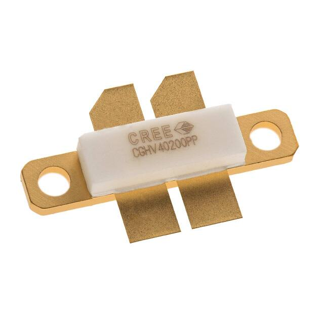
CGHV40200PP
200 W, 50 V, GaN HEMT
Description
Cree’s CGHV40200PP is an unmatched, gallium nitride (GaN) high
electron mobility transistor (HEMT). The CGHV40200PP, operating
from a 50 volt rail, offers a general purpose, broadband solution
to a variety of RF and microwave applications. GaN HEMTs offer
high efficiency, high gain and wide bandwidth capabilities making
the CGHV40200PP ideal for linear and compressed amplifier
circuits. The transistor is available in a 4-lead flange package.
Package Type: 440199
PN: CGHV40200PP
Typical Performance Over 1.7-1.9 GHz (TC = 25˚C), CW
Parameter
1.7 GHz
1.8 GHz
1.9 GHz
Units
Small Signal Gain
21.7
21.0
20.1
dB
Gain @ PIN = 38 dBm
16.5
16.1
15.4
dB
POUT @ PIN = 38 dBm
270
250
218
W
Drain Efficiency @ PIN = 38 dBm
64
67
65
%
Features
Applications
•
•
•
•
•
•
•
•
•
•
Up to 3.0 GHz Operation
21 dB Small Signal Gain at 1.8 GHz
250 W typical PSAT
67% Efficiency at PSAT
50 V Operation
2-Way Private Radio
Broadband Amplifiers
Cellular Infrastructure
Test Instrumentation
Class A, AB, Linear amplifiers suitable for
OFDM, W-CDMA, EDGE, CDMA waveforms
Large Signal Models Available for ADS and MWO
Rev 1.4 – November 2021
4600 Silicon Drive | Durham, NC 27703 | wolfspeed.com
�CGHV40200PP
2
Absolute Maximum Ratings (not simultaneous) at 25˚C Case Temperature
Parameter
Symbol
Rating
Units
Conditions
Drain-Source Voltage
VDSS
150
Volts
25˚C
Gate-to-Source Voltage
VGS
-10, +2
Volts
25˚C
Storage Temperature
TSTG
-65, +150
˚C
Operating Junction Temperature
TJ
225
˚C
Maximum Forward Gate Current
IGMAX
41.6
mA
25˚C
Maximum Drain Current
IDMAX
8.7
A
25˚C
Soldering Temperature
TS
245
˚C
τ
40
in-oz
Thermal Resistance, Junction to Case
RθJC
0.94
˚C/W
Case Operating Temperature
TC
-40, +70
˚C
1
1
2
Screw Torque
3
3,4
85˚C
Notes:
1
Current limit for long term, reliable operation per side of the device
2
Refer to the Application Note on soldering at wolfspeed.com/rf/document-library
3
CGHV40200PP at PDISS = 166 W
4
See also, the Power Dissipation De-rating Curve on Page
Electrical Characteristics (TC = 25˚C)
Characteristics
Symbol
Min.
Typ.
Max.
Units
Conditions
DC Characteristics1
Gate Threshold Voltage
VGS(th)
-3.8
-3.0
-2.3
VDC
VDS = 10 V, ID = 41.6 mA
Gate Quiescent Voltage
VGS(Q)
–
-2.7
–
VDC
VDS = 50 V, ID = 2.0 A
Saturated Drain Current2
IDS
27.0
38.7
–
A
VDS = 6.0 V, VGS = 2.0 V
Drain-Source Breakdown Voltage
VBR
125
–
–
VDC
VGS = -8 V, ID = 41.6 mA
RF Characteristics3,4 (TC = 25˚C, F0 = 1.8 GHz unless otherwise noted)
Small Signal Gain
GSS
17.75
20.0
–
dB
VDD = 50 V, IDQ = 1.2 A, PIN = 10 dBm
Power Gain
PG
15.05
16.0
-
dB
VDD = 50 V, IDQ = 1.2 A, PIN = 38 dBm
Power Output
POUT
200
250
–
W
VDD = 50 V, IDQ = 1.2 A, PIN = 38 dBm
Drain Efficiency5
η
60
69
–
%
VDD = 50 V, IDQ = 1.2 A, PIN = 38 dBm
VSWR
–
–
3:1
Y
No damage at all phase angles,
VDD = 50 V, IDQ = 1.2 A, POUT = 200 W CW
Input Capacitance
CGS
–
29.3
–
pF
VDS = 28 V, Vgs = -8 V, f = 1 MHz
Output Capacitance
CDS
–
7.3
–
pF
VDS = 28 V, Vgs = -8 V, f = 1 MHz
Feedback Capacitance
CGD
–
0.61
–
pF
VDS = 28 V, Vgs = -8 V, f = 1 MHz
Output Mismatch Stress
Dynamic Characteristics6
Notes:
1
Measured on wafer prior to packaging per side of device
2
Scaled from PCM data
3
Measured in CGHV40200PP-TB
4
IDQ of 1.2 A is by biasing each device at 0.6 A
5
Drain Efficiency = POUT / PDC
6
Capacitance values are for each side of the device
Rev 1.4 – November 2021
4600 Silicon Drive | Durham, NC 27703 | wolfspeed.com
�CGHV40200PP
3
Typical Performance
Figure 1. Gain and Return
Losses vs Frequency measured in CGHV40200PP-TB
Small Signal Gain and Return Loss vs. Frequency
VDD = 50 V, IDQ = 1.2
A, Freq = 1500 - 2000 MHz
CGHV40200PP
VDD = 50V, IDQ=2*0.60A
30
Gain, Return Loss (dB)
Gain and Return Losses (dB)
25
20
15
10
5
0
-5
S21
-10
S11
-15
S22
-20
1500
1550
1600
1650
1700
1750
1800
1850
1900
1950
2000
Frequency (GHz)
Frequency (MHz)
100
270
90
240
80
210
70
180
60
150
50
120
40
Pout
90
EFF
60
20
10
30
0
1.70
30
Drain Efficiency(%)
300
Drain Efficiency (%)
Pout
(Watts)
Pout (Watts)
Figure 2. Output Power and Drain Efficiency vs Frequency measured in CGHV40200PP-TB
CW Operation, VDD = 50 V, IDQ = 1.2 A, Output Power @ PIN = 38 dBm
1.73
1.75
1.78
1.80
Frequency (GHz)
1.83
1.85
1.88
0
1.90
Frequency (GHz)
Rev 1.4 – November 2021
4600 Silicon Drive | Durham, NC 27703 | wolfspeed.com
�CGHV40200PP
4
Typical Performance
Figure 3. Gain and Drain Efficiency vs Output Power measured in CGHV40200PP-TB
CW Operation, VDD = 50 V, IDQ = 1.2 A
100
90
20
80
17.5
70
15
60
12.5
50
10
Drain Efficiency (%)
22.5
Drain Efficiency (%)
Gain (dB)
Gain (dB)
25
40
1.70 Gain
7.5
30
1.80 Gain
1.90 Gain
5
20
1.70 EFF
1.80 EFF
2.5
0
10
1.90 EFF
35
37
39
41
43
45
47
49
Output Power (dBm)
Output
Power (dBm)
51
53
55
0
Figure 4. Simulated Maximum
Avaliable
Gain
of the CGHV40200PP
Simulated Maximum
Avaliable Gain
and and
K-factorK-factor
of the CGHV40200PP
VDD = 50V, IDQ=2*0.60A
VDD = 50 V, IDQ = 1.2 A
5
50
Gmax
45
K
40
4
3
K-factor
30
25
2
20
K-factor
MAG (dB)
MAG (dB)
35
15
10
1
5
0
0
1
2
3
Frequency (GHz)
4
5
6
0
Frequency (GHz)
Electrostatic Discharge (ESD) Classifications
Parameter
Symbol
Class
Test Methodology
Human Body Model
HBM
1A > 250 V
JEDEC JESD22 A114-D
Charge Device Model
CDM
1 < 200 V
JEDEC JESD22 C101-C
Rev 1.4 – November 2021
4600 Silicon Drive | Durham, NC 27703 | wolfspeed.com
�CGHV40200PP
5
CGHV40200PP-AMP1 Demonstration Amplifier Circuit Bill of Materials
Designator
Description
Qty
R1,2
RES,1/4W,1206 1%, 0 OHM
2
R5, R6, R7,R11, R12, R13
RES, 1/16W, 0603, 1%, 5.1 Ohms
6
R3, R4, R9, R10
RES 5.1 OHM 1/8W 5% 0805 SMD
4
R15, R16, R17, R18
RES SMD 10 OHM 1% 2W 2512
4
R8,14
RES SMD 150 OHM 5% 1W 2512
2
C48,49
CAP, 0.1PF, +/- 0.05pF, 0805, ATC, 600F
2
C16
CAP, 0.8pF, +/-0.05pF, 0805, ATC
1
C27
CAP, 1.2pF, +/-0.1pF, 0603, ATC
1
C24
CAP, 1.2pF, +/-0.1pF, 0805, ATC
1
C15
CAP, 1.0pF, +/-0.1pF, 0603, ATC
1
C26
CAP, 1.5pF,+/-0.1pF, 0603, ATC
1
C25
CAP, 2.0pF, +/-0.1pF, 0805, ATC
1
C17
CAP, 3.9pF,+/-0.25pF, 0805, ATC
1
C28,29,36,37, 42, 46
CAP, 5.1pF, +/-0.05pF, 0805, ATC600F
4
C5,6,38,39
CAP, 5.6 PF +/- 0.1 pF, 0805, ATC 600F
4
C4,7,31,35
CAP, 20PF ±5% 250V 0805, ATC600F
4
C32,33,44,47
CAP, 100 PF +/- 5%, 250V, 0805, ATC 600F
4
C2,3,8,9,13,18,30, 34,40,41, 43, 45
CAP, 1000PF, +/-10%, 0805, X7R, 100V, TEMP STBL
12
C1,11,14,19,22,23,
CAP, 10000PF, +/-10%, 0805, X7R, 100V, TEMP STBL
6
C21
CAP, 0.1uF, +/-10%, 250V, 1206, X7R
1
C10,12
CAP CER 10UF 25V X7R 1206
2
C20
CAP, 330 UF, +/-20%, 100V, ELECTROLYTIC, CASE SIZE K16
1
L6,7, 9,10,12, 13
IND, 12NH, 2%, 0908SQ-12NGL
6
L2, 3
IND, 27NH, 2%, 0908SQ-27NGL
2
L11
CABLE ,18 AWG, 4.2”
1
L1,4
FERRITE BEAD 600 OHM 0603 1LN
2
L5,8
FERRITE BEAD 72 OHM 1806 1LN
2
J2,3
CONN, SMA, PANEL MOUNT JACK, FLANGE, 4-HOLE, BLUNT POST
2
J1
HEADER RT>PLZ .1CEN LK 9POS
1
J4,5
CONN SMA JACK STR 50 OHM SMD
2
PCB, Rogers 6035HTC 0.020” THK, CGHV40200PP 1.35-1.85 GHz
1
BASEPLATE, AL, 4.80 X 3.60 X 0.49, ALTERNATE HOLE PATTERN
1
2-56 SOC HD SCREW 1/4 SS
4
#2 SPLIT LOCKWASHER SS
4
CGHV40200PPP
1
Rev 1.4 – November 2021
4600 Silicon Drive | Durham, NC 27703 | wolfspeed.com
�CGHV40200PP
6
CGHV40200F Typical Performance
Figure 5. Small Signal Gain and Return Losses vs Frequency
measured in the CGHV40200PP-AMP1 Broadband Amplifier Circuit
VDD = 50 V, IDQ = 1.2 A
30
20
S21, S11, S22 (dB)
10
0
-10
-20
S11
S22
-30
-40
S21
1
1.1
1.2
1.3
1.4
1.5
1.6
1.7
1.8
1.9
2
Frequency (GHz)
350
100
300
85
250
70
200
55
Fix. 2 pout
150
40
Fix. 2 Gain
Fix. 2 Eff
100
25
50
0
1.30
Gain (dB)
Output Power (dBm), Drain Efficiency (%)
Figure 6. Saturated Output Power Gain, and Drain Efficiency vs Frequency of the CGHV40200PP
measured in the CGHV40200PP-AMP1 Broadband Amplifier Circuit
VDD = 50V, IDQ = 1 A, CW, PSAT, IG = 0 mA
10
1.35
1.40
1.45
1.50
1.55
1.60
1.65
1.70
1.75
1.80
1.85
-5
1.90
Frequency (GHz)
Rev 1.4 – November 2021
4600 Silicon Drive | Durham, NC 27703 | wolfspeed.com
�CGHV40200PP
7
CGHV40200PP-AMP1 Demonstration Amplifier Circuit Schematic
CGHV40200PP-AMP1 Demonstration Amplifier Circuit Outline
Rev 1.4 – November 2021
4600 Silicon Drive | Durham, NC 27703 | wolfspeed.com
�CGHV40200PP
8
Simulated Source and Load Impedances
D1
Frequency (MHz) Z Source (1,2) Z Load (1,2)
Z Source 1
Z Load 1
G1
S
500
2.9 +j4.8
12.8 +j7.3
1000
0.8 +j1.5
9.1 +j5.1
1500
0.9 +-j0.6
5.5 +j3.8
2000
1.1 -j2.2
4.4 +j2.0
2500
1.8 -j4.0
3.8 +j0.5
Note 1. VDD = 50 V, IDQ = 2 x 0.6 A in the 440199 package
Note 2. Optimized for power gain, PSAT and PAE
Note 3. When using this device at low frequency, series resistors
should be used to maintain amplifier stability
G2
Z Source 2
Z Load 2
D2
Power Dissipation (W)
CGHV40200PP Power Dissipation De-rating Curve
Maximum Case Temperature (°C)
Note 1. Area exceeds Maximum Case Operating Temperature (See Page 2)
Rev 1.4 – November 2021
4600 Silicon Drive | Durham, NC 27703 | wolfspeed.com
�CGHV40200PP
9
Product Dimensions CGHV40200PP (Package Type 440199)
Rev 1.4 – November 2021
4600 Silicon Drive | Durham, NC 27703 | wolfspeed.com
�CGHV40200PP
10
Part Number System
CGHV40200PP
Package
Power Output (W)
Upper Frequency (GHz)
Cree GaN High Voltage
Table 1.
Parameter
Value
Units
Upper Frequency1
2.5
GHz
Power Output
200
W
Package
Push Pill
-
Note1: Alpha characters used in frequency code indicate a value
greater than 9.9 GHz. See Table 2 for value
Table 2.
Rev 1.4 – November 2021
Character Code
Code Value
A
0
B
1
C
2
D
3
E
4
F
5
G
6
H
7
J
8
K
9
Examples:
1A = 10.0 GHz
2H = 27.0 GHz
4600 Silicon Drive | Durham, NC 27703 | wolfspeed.com
�CGHV40200PP
11
Product Ordering Information
Order Number
Description
Unit of Measure
CGHV40200PP
GaN HEMT
Each
CGHV40200PP-AMP1
Test board with GaN HEMT installed
Each
Rev 1.4 – November 2021
Image
4600 Silicon Drive | Durham, NC 27703 | wolfspeed.com
�CGHV40200PP
12
For more information, please contact:
4600 Silicon Drive
Durham, North Carolina, USA 27703
www.wolfspeed.com/RF
Sales Contact
RFSales@wolfspeed.com
RF Product Marketing Contact
RFMarketing@wolfspeed.com
Notes
Disclaimer
Specifications are subject to change without notice. Cree, Inc. believes the information contained within this data sheet
to be accurate and reliable. However, no responsibility is assumed by Cree for any infringement of patents or other rights
of third parties which may result from its use. No license is granted by implication or otherwise under any patent or patent rights of Cree. Cree makes no warranty, representation or guarantee regarding the suitability of its products for any
particular purpose. “Typical” parameters are the average values expected by Cree in large quantities and are provided for
information purposes only. These values can and do vary in different applications and actual performance can vary over
time. All operating parameters should be validated by customer’s technical experts for each application. Cree products
are not designed, intended or authorized for use as components in applications intended for surgical implant into the
body or to support or sustain life, in applications in which the failure of the Cree product could result in personal injury
or death or in applications for planning, construction, maintenance or direct operation of a nuclear facility.
© 2017 - 2020 Cree, Inc. All rights reserved. Wolfspeed® and the Wolfspeed logo are registered trademarks of Cree, Inc.
Rev 1.4 – November 2021
4600 Silicon Drive | Durham, NC 27703 | wolfspeed.com
�