HGTG30N60B3
Data Sheet
November 2013
600 V, NPT IGBT
Features
The HGTG30N60B3 combines the best features of high
input impedance of a MOSFET and the low on-state
conduction loss of a bipolar transistor. The IGBT is ideal for
many high voltage switching applications operating at
moderate frequencies where low conduction losses are
essential, such as: UPS, solar inverter and power supplies.
• 30 A, 600 V, TC = 110°C
• Low Saturation Voltage: VCE(sat) = 1.45 V @ IC = 30 A
• Typical Fall Time. . . . . . . . 90ns at TJ = 150°C
• Short Circuit Rating
• Low Conduction Loss
Formerly Developmental Type TA49170.
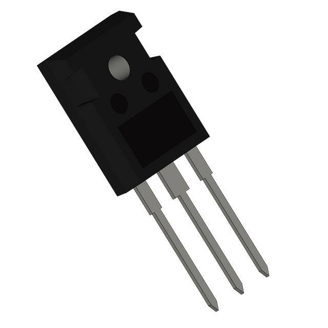
Packaging
Ordering Information
PART NUMBER
HGTG30N60B3
JEDEC STYLE TO-247
PACKAGE
TO-247
BRAND
G30N60B3
NOTE: When ordering, use the entire part number.
Symbol
C
G
C
E
TO-247
G
E
©2001 Fairchild Semiconductor Corporation
HGTG30N60B3 Rev. C1
1
www.fairchildsemi.com
�HGTG30N60B3
Absolute Maximum Ratings TC = 25oC, Unless Otherwise Specified
Ratings
UNIT
600
V
At TC = 25oC . . . . . . . . . . . . . . . . . . . . . . . . . . . . . . . . . . . . . . . . . . . . . . . . . . . . . . . . . IC25
60
A
At TC = 110oC . . . . . . . . . . . . . . . . . . . . . . . . . . . . . . . . . . . . . . . . . . . . . . . . . . . . . . . IC110
30
A
Collector Current Pulsed (Note 1) . . . . . . . . . . . . . . . . . . . . . . . . . . . . . . . . . . . . . . . . . . . ICM
220
A
Gate to Emitter Voltage Continuous. . . . . . . . . . . . . . . . . . . . . . . . . . . . . . . . . . . . . . . . . VGES
20
V
Gate to Emitter Voltage Pulsed . . . . . . . . . . . . . . . . . . . . . . . . . . . . . . . . . . . . . . . . . . . VGEM
30
V
Switching Safe Operating Area at TJ = 150oC (Figure 2) . . . . . . . . . . . . . . . . . . . . . . . SSOA
60 A at 600 V
Collector to Emitter Voltage . . . . . . . . . . . . . . . . . . . . . . . . . . . . . . . . . . . . . . . . . . . . . .BVCES
Collector Current Continuous
Power Dissipation Total at TC = 25oC . . . . . . . . . . . . . . . . . . . . . . . . . . . . . . . . . . . . . . . . . PD
208
W
Power Dissipation Derating TC > 25oC . . . . . . . . . . . . . . . . . . . . . . . . . . . . . . . . . . . . . . . . . .
1.67
W/oC
Reverse Voltage Avalanche Energy . . . . . . . . . . . . . . . . . . . . . . . . . . . . . . . . . . . . . . . . EARV
100
mJ
Operating and Storage Junction Temperature Range . . . . . . . . . . . . . . . . . . . . . . . . TJ, TSTG
-55 to 150
oC
Maximum Lead Temperature for Soldering . . . . . . . . . . . . . . . . . . . . . . . . . . . . . . . . . . . . . TL
260
oC
Short Circuit Withstand Time (Note 2) at VGE = 12 V . . . . . . . . . . . . . . . . . . . . . . . . . . . . .tSC
4
s
Short Circuit Withstand Time (Note 2) at VGE = 10 V . . . . . . . . . . . . . . . . . . . . . . . . . . . . .tSC
10
s
CAUTION: Stresses above those listed in “Absolute Maximum Ratings” may cause permanent damage to the device. This is a stress only rating and operation of the
device at these or any other conditions above those indicated in the operational sections of this specification is not implied.
NOTES:
1. Pulse width limited by maximum junction temperature.
2. VCE(PK) = 360 V, TJ = 125oC, RG = 3
Electrical Specifications
TC = 25oC, Unless Otherwise Specified
PARAMETER
SYMBOL
TEST CONDITIONS
MIN
TYP
MAX
UNIT
Collector to Emitter Breakdown Voltage
BVCES
IC = 250 A, VGE = 0 V
600
-
-
V
Emitter to Collector Breakdown Voltage
BVECS
IC = -10 mA, VGE = 0 V
20
-
-
V
TC = 25oC
-
-
250
A
TC = 150oC
TC = 25oC
TC = 150oC
-
-
3.0
mA
-
1.45
1.9
V
-
1.7
2.1
V
4.2
5.0
6.0
V
-
-
250
nA
VCE (PK) = 480 V
200
-
-
A
VCE (PK) = 600 V
60
-
-
A
IC = IC110, VCE = 0.5 BVCES
-
7.2
-
V
IC = IC110,
VCE = 0.5 BVCES
VGE = 15 V
-
170
190
nC
VGE = 20 V
-
230
250
nC
-
36
-
ns
-
25
-
ns
-
137
-
ns
-
58
-
ns
-
500
-
J
Collector to Emitter Leakage Current
Collector to Emitter Saturation Voltage
Gate to Emitter Threshold Voltage
Gate to Emitter Leakage Current
Switching SOA
ICES
VCE(SAT)
VGE(TH)
VCE = BVCES
IC = IC110,
VGE = 15 V
IC = 250 A, VCE = VGE
IGES
VGE = 20 V
SSOA
TJ = 150oC,
RG = 3
VGE = 15 V,
L = 100 H
Gate to Emitter Plateau Voltage
On-State Gate Charge
Current Turn-On Delay Time
Current Rise Time
Current Turn-Off Delay Time
Current Fall Time
VGEP
QG(ON)
td(ON)I
trI
td(OFF)I
tfI
IGBT and Diode at TJ = 25oC
ICE = IC110
VCE = 0.8 BVCES
VGE = 15 V
RG= 3
L = 1 mH
Test Circuit (Figure 17)
Turn-On Energy (Note 4)
EON1
Turn-On Energy (Note 4)
EON2
-
550
800
J
Turn-Off Energy (Note 3)
EOFF
-
680
900
J
©2001 Fairchild Semiconductor Corporation
HGTG30N60B3 Rev. C1
2
www.fairchildsemi.com
�HGTG30N60B3
Electrical Specifications
TC = 25oC, Unless Otherwise Specified (Continued)
PARAMETER
SYMBOL
Current Turn-On Delay Time
td(ON)I
Current Rise Time
trI
Current Turn-Off Delay Time
td(OFF)I
Current Fall Time
tfI
TEST CONDITIONS
MIN
TYP
MAX
UNIT
-
32
-
ns
-
24
-
ns
-
275
320
ns
-
90
150
ns
-
500
-
J
J
IGBT and Diode at TJ = 150oC
ICE = IC110
VCE = 0.8 BVCES
VGE = 15 V
RG= 3
L = 1 mH
Test Circuit (Figure 17)
Turn-On Energy (Note 4)
EON1
Turn-On Energy (Note 4)
EON2
-
1300
1550
Turn-Off Energy (Note 3)
EOFF
-
1600
1900
J
Thermal Resistance Junction To Case
RJC
-
-
0.6
oC/W
NOTES:
3. Turn-Off Energy Loss (EOFF) is defined as the integral of the instantaneous power loss starting at the trailing edge of the input pulse and ending
at the point where the collector current equals zero (ICE = 0A). All devices were tested per JEDEC Standard No. 24-1 Method for Measurement
of Power Device Turn-Off Switching Loss. This test method produces the true total Turn-Off Energy Loss.
4. Values for two Turn-On loss conditions are shown for the convenience of the circuit designer. EON1 is the turn-on loss of the IGBT only. EON2
is the turn-on loss when a typical diode is used in the test circuit and the diode is at the same TJ as the IGBT. The diode type is specified in
Figure 17.
Unless Otherwise Specified
ICE, COLLECTOR TO EMITTER CURRENT (A)
ICE , DC COLLECTOR CURRENT (A)
60
VGE = 15V
50
40
30
20
10
0
25
75
50
100
125
150
225
TJ = 150oC, RG = 3, VGE = 15V, L =100H
200
175
150
125
100
75
50
25
0
0
TC , CASE TEMPERATURE (oC)
tSC , SHORT CIRCUIT WITHSTAND TIME (s)
fMAX, OPERATING FREQUENCY (kHz)
10
TC
fMAX1 = 0.05 / (td(OFF)I + td(ON)I)
o
fMAX2 = (PD - PC) / (EON2 + EOFF) 75 C
oC
75
PC = CONDUCTION DISSIPATION
110oC
(DUTY FACTOR = 50%)
110oC
RØJC = 0.6oC/W, SEE NOTES
VGE
15V
10V
15V
10V
0.1
5
10
20
40
60
FIGURE 3. OPERATING FREQUENCY vs COLLECTOR TO
EMITTER CURRENT
©2001 Fairchild Semiconductor Corporation
500
400
600
700
20
500
VCE = 360V, RG = 3, TJ = 125oC
18
450
400
16
ISC
14
350
12
300
10
250
tSC
200
8
150
6
10
11
12
13
14
15
VGE , GATE TO EMITTER VOLTAGE (V)
ICE, COLLECTOR TO EMITTER CURRENT (A)
HGTG30N60B3 Rev. C1
300
FIGURE 2. MINIMUM SWITCHING SAFE OPERATING AREA
TJ = 150oC, RG = 3, L = 1mH,
V CE = 480V
1
200
VCE, COLLECTOR TO EMITTER VOLTAGE (V)
FIGURE 1. DC COLLECTOR CURRENT vs CASE
TEMPERATURE
100
100
ISC, PEAK SHORT CIRCUIT CURRENT (A)
Typical Performance Curves
FIGURE 4. SHORT CIRCUIT WITHSTAND TIME
3
www.fairchildsemi.com
�HGTG30N60B3
Unless Otherwise Specified (Continued)
ICE, COLLECTOR TO EMITTER CURRENT (A)
ICE, COLLECTOR TO EMITTER CURRENT (A)
Typical Performance Curves
225
DUTY CYCLE
很抱歉,暂时无法提供与“HGTG30N60B3”相匹配的价格&库存,您可以联系我们找货
免费人工找货