LSI/CSI
UL
®
LS7213R
LSI Computer Systems, Inc. 1235 Walt Whitman Road, Melville, NY 11747
(631) 271-0400 FAX (631) 271-0405
A3800
September 2006
PROGRAMMABLE DIGITAL DELAY TIMER
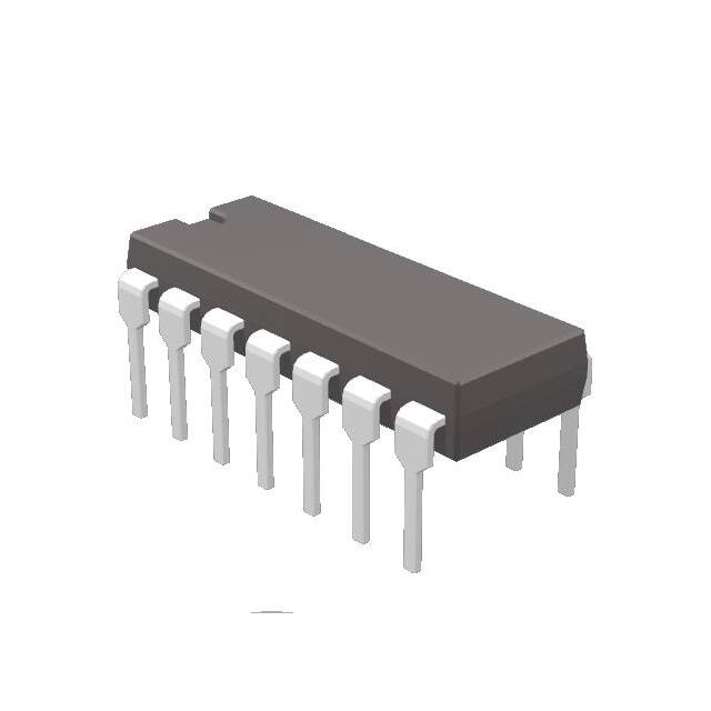
PIN ASSIGNMENT
TOP VIEW
14
V DD (+V)
2
13
OUT1
D1
3
12
OUT2
FLASHEN
4
11
RESET
10
RC
On-Delay (OND) Mode
A positive transition at the Trigger input starts the on-delay timer. At
the end of the delay, Out1 switches low and Out2 switches high. A
negative transition at the Trigger input immediately aborts any ondelay in progress. If the Trigger input is switched low, Out1 if low
will switch high and Out2 if high will switch low without delay. The
states of Out2 in the preceding description applies only if FlashEn
input is low at the time of the Trigger input transition. See the Out2
pin section for a complete description.
Off-Delay (OFD) Mode
A negative transition at the Trigger input starts the off-delay timer.
At the end of the delay, Out1 switches high and Out2 switches low.
A positive transition at the Trigger input immediately aborts any offdelay in progress. If the Trigger input is switched high, Out1 if high
will switch low and Out2 if low will switch high without delay. The
states of Out2 in the preceding description applies only if FlashEn
input is low at the time of the Trigger input transition. See the Out2
pin section for a complete description.
Dual-Delay (DLD) Mode
In Dual-Delay mode, the delay is generated for both positive and
negative transitions at the Trigger input. A positive transition at the
Trigger input starts the on-delay timer and aborts any off-delay timing in progress. At the end of the delay Out1 switches low and Out2
switches high. A negative transition at the Trigger input starts the
off-delay timer and aborts any on-delay timing in progress. At the
end of the delay Out1 switches high and Out2 switches low. The
states of Out2 in the preceding description applies only if FlashEn
input is low at the time of the Trigger input transition. See the Out2
pin section for a complete description.
7213R-090806-1
D2
LS7213R
On-Delay (OND), Off-Delay (OFD), Dual-Delay (DLD) and
One-Shot (OST). These modes are described below:
1
A
5
B
6
9
CAP
V SS (-V)
7
8
TRIGGER
APPLICATIONS
Time delay relays for HVAC equipment and industrial controls.
DESCRIPTION
The LS7213R is a CMOS integrated circuit for generating programmable time-delays. The delay is initiated by a logic transition
at the Trigger input and the completion of the delay is marked by a
change of status at the Out1 and the Out2 outputs. Three inputs,
D1, D2 and D3 select 1-of-8 scale factors, s. The delay, td is related
to s by the expression, td = s/f rc, where frc is the frequency at the
RC input produced by an internal oscillator. An external resistorcapacitor pair connected to the RC pin controls the oscillator frequency. There are four modes of operation selected by inputs A
and B. The operating modes are:
D3
LSI
FEATURES:
• Eight timing ranges • Four modes
• RC controlled on-chip oscillator
• Power-On-Reset (POR)
• Reset input for delay abort
• Complementary outputs
• Delay-in-Progress Indicator output
• LS7213R (DIP), LS7213R-S (SOIC) - See Figure 1
FIGURE 1
One-Shot (OST) Mode
A positive transition at the Trigger input causes Out1 to switch
low and Out2 to switch high immediately and start the one-shot
delay timer. At the end of the delay Out1 switches high and Out2
switches low. Thus in effect, a positive transition at the Trigger input produces a negative pulse at Out1 and a positive pulse at
Out2. The one-shot delay timer is restarted with every positive
trigger transition, thus rendering the Out1 and Out2 pulse-widths
stretchable to any duration by periodic re-trigger. A negative transition at the Trigger input has no effect. The states of Out2 in the
preceding description applies only if FlashEn input is low at the
time of the Trigger input transition. See the Out2 pin section for a
complete description.
INPUTS/OUTPUTS
Following is a description of all the input/output pins and their
functions.
Delay Select Inputs: D1, D2, D3 (Pin 3, Pin 2, Pin 1)
The logic states applied to these three inputs enable the user to
select a scale factor, s, for generating a delay, td, fromTrigger input to Out1/Out2 outputs according to Table1. The delay is given
by the expression:
td = s/frc,
where, s is the scale factor, and frc is the oscillator frequency at
the RC input. The sample delays in Table1 are based on an oscillator frequency, frc = 10kHz.
TABLE 1. Delay Selection
D3
0
0
0
0
1
1
1
1
D2
0
0
1
1
0
0
1
1
D1
0
1
0
1
0
1
0
1
s
1x10³
1x10⁴
1x10⁵
60x103
60x104
60x105
3600x103
3600x104
td (= s/frc)
0.1sec
1.0sec
10.0sec
0.1min
1.0min
10.0min
0.1hr
1.0hr
D1, D2 and D3 inputs have internal pull-down resistors
�Mode Select Inputs: A, B (Pin 5, Pin 6)
The four operating modes are selected by inputs A and B
cording to Table 2.
ac-
TABLE 2. Mode Selection
A
0
0
1
1
B
0
1
0
1
Mode
On-Delay (OND)
Off-Delay (OFD)
Dual-Delay (DLD)
One-Shot (OST)
Inputs A and B have internal pull-down resistors.
Driver Outputs: Out1, Out2 (Pin 13, Pin 12)
Out1 is an output for driving DC loads requiring high current sink,
such as relays, power transistors, etc. In steady-state condition
Out1, with the exception of one-shot mode, is always inverse in polarity with respect to the Trigger input. Depending on the operating
mode, the steady-state condition is reached immediately or after a
specified delay following a change of state at the Trigger input. In
one-shot mode, Out1 is always at logic high in the steady state, independent of the logic state of the Trigger input.
Out2 operates in two different modes depending on the state of the
FlashEn input.
If Flashen is at logic low then:
Out2 operates exactly as Out1 but with inverse polarity. In this
mode, Out2 is an output for driving DC loads requiring high current
source, such as relays, power transistors, etc. In steady-state condition Out2, with the exception of one-shot mode, is always at the
same polarity as the Trigger input. Depending on the operating
mode, the steady-state condition is reached immediately or after a
specified delay following a change of state at the Trigger input. In
one-shot mode Out2 is always at logic low in the steady state, independent of the logic state of the Trigger input.
If Flashen is at logic high then:
Out2 operates as a delay-in-progress indicator by generating periodic positive pulses during a delay timing. The pulse-rate, fpf and
the pulse-width tpf at Out2 is controlled by an internal oscillator
whose frequency, fcf,, is set by a capacitor connected to the Cap
input. fpf and ff, are related by the following expressions:
fpf = 20/fcf,
for scale factors 1x10³ and 1x10⁴ and
fpf = 100/fcf,
for all other scale factors.
The pulse-width, tpf for both pulse-rates is given by:
tpf = 2/fcf
At the end of timeout, Out2 returns to logic low with the cessation
of pulses.
NOTE:
Since the delay is restarted on both high and low transitions of the
Trigger in Dual Delay Mode, the Delay-In-Progress indicator will always complete the delay selection from the last Trigger transition.
Timer Start Input: Trigger (Pin 8)
Any logic transition at the Trigger input, positive or negative causes the outputs Out1 and Out2 to switch with or without delay, depending on the operating mode.
Any transition of the Trigger input also causes the logic states of
the following inputs to be strobed into internal latches: A, B, D1,
D2, D3 and FlashEn. This prevents any changes at any of these
inputs from disrupting the timer when a timeout is in progress.
See the description of modes on Page1 and Out1, Out2 section on
Page 2 for a complete description of the Trigger input.
TheTrigger input has an internal pull-down resistor.
7213R-120205-2
Flash Enable Input: FlashEn (Pin 4)
The FlashEn input modifies the operation of Out2 to function in
one of two modes.
When FlashEn = 0, Out2 functions exactly as Out1 but with inverse polarity from Out1. When FlashEn = 1, Out2 functions as a
flashing delay-in-progress indicator. In this mode periodic positive
pulses are generated at Out2 during a delay timing which can be
used to produce a flashing LED display for user feedback. For a
complete description see Out2 section on Page 2. The Fashen
input has an internal pull-down resistor.
Master Clear Input: Reset (Pin 11)
When Reset is brought to logic high, all timing functions are
aborted, the timer is cleared, Out1 is forced high and Out2 is
forced low. Switching the Reset input low causes the mode select
inputs, the delay select inputs, the FlashEn input and the Trigger
input to be sampled by internal logic. Following this, any inconsistencies between the Trigger input and the Out1 and Out2
outputs are resolved and the steady state is reached with or without delay based on the status of the mode select inputs. For example, if the Trigger input is high, the FlashEn input is low and
the mode is off-delay when the Reset input is switched from high
to low, Out1 and Out2 will immediately be switched low and high,
respectively, from its forced reset condition. In this example if the
mode is on-delay instead of off-delay, then Out1 and Out2 will be
switched after the completion of the programmed delay td.
It should be noted here that the states of Out1 and Out2 in the
reset condition and One-Shot mode steady state condition are
the same namely, Out1 = 1 and Out2 = 0. Because of this, in
one-shot mode, no change in Out1 and Out2 takes place when
the Reset input is switched low, irrespective of the status of the
Trigger input. The Reset input has an internal pull-down resistor.
NOTE: A POR circuit (See Fig. 2) generates a reset upon power
up that produces the same conditions described for Reset
(Pin 11).
Timer Oscillator Input: RC (Pin 10)
A resistor-capacitor pair connected to the RC input serves as the
basic timing element for the delay timer oscillator.
The oscillator frequency is given by the expression:
frc = 1/0.9RC,
where R and C are the resistor and the capacitor values at the
RC input.
The delay, td, is given by the expression:
td = s/frc,
where s is the scale factor selected by inputs D1, D2 and D3.
Flash Oscillator Input: Cap (Pin 9)
A capacitor, C, connected from the Cap input to ground regulates
an internal flash oscillator frequency according to the relation:
fcf = (k/C) x 10-6
where k is a V DD dependent constant ranging in value between
2.1 at V DD = 3V to 4.8 at V DD = 5V. Chip to chip tolerance of fcf is
+ 10% at fixed V DD. The flash oscillator frequency controls the
pulse-rate, f pf and the pulse width, tpf at Out2 in flash mode according to the following relationships:
fpf = 20/fcf,
for scale factors 1x10³ and 1x10⁴ and
fpf = 100/fcf,
for all other scale factors; and for the pulse-width,
tpf = 2/fcf, for all scale factors.
Power Supplies VDD, Vss (Pin 14, Pin 7)
VDD is the power supply positive terminal and Vss is the negative
or ground terminal.
�ABSOLUTE MAXIMUM RATINGS:
(All voltages referenced to VSS)
SYMBOL
VDD
VIN
TA
TSTG
DC Supply Voltage
Voltage (Any Pin)
Operating Temperature
Storage Temperature
VALUE
+7
VSS - 0.3 to VDD + 0.3
-20 to +85
-65 to +150
UNIT
V
V
°C
°C
ELECTRICAL CHARACTERISTICS (Voltages referenced to Vss unless specified otherwise)
Characteristic
SYMBOL
Supply Voltage
VDD
Supply Current
IDD
3
4
5
Min
3.0
-
-20°C
Max
5.5
75
125
190
Min
3.0
-
+25°C
Max
5.5
65
100
150
Min
3.0
-
+85°C
Max
5.5
50
85
140
3
4
5
3
4
5
3
4
5
3
4
5
-
1.6
2.0
2.7
0.8
1.2
1.5
1.5
1.9
2.4
-
1.0
1.3
1.6
1.6
2.0
2.7
0.8
1.2
1.5
0.4
0.5
0.5
1.5
1.9
2.4
-
2.0
2.6
3.3
1.2
1.8
2.1
1.2
1.4
1.8
1.0
1.3
1.6
1.6
2.0
2.7
0.8
1.2
1.5
1.5
1.9
2.4
-
1.0
1.3
1.6
V
V
V
V
V
V
V
V
V
V
V
V
V
V
V
3
4
5
0.9
3.5
8.0
5
2.5
6.0
12.0
0.8
3.0
7.0
5
2.0
5.0
10.0
0.5
2.0
5.0
10
1.6
4.0
8.0
nA
µA
µA
µA
3
4
5
3
4
5
3
4
5
3
4
5
12.0
14.0
18.0
1.8
3.0
3.5
5.4
7.8
9.0
9.0
13.0
15.0
-
10.0
12.0
15.0
1.5
2.5
3.0
4.5
6.5
7.5
8.0
11.0
13.0
-
7.0
9.0
10.0
1.0
1.6
2.0
3.0
4.5
5.5
6.0
8.0
9.0
-
mA
mA
mA
mA
mA
mA
mA
mA
mA
mA
mA
mA
3
4
5
6.8k
4.7k
3.9k
6.0
10M
10M
10M
8.2k
5.6k
4.7k
5.0
10M
10M
10M
10.0k
6.8k
5.6k
4.0
10M
10M
10M
MHz
Ω
Ω
Ω
-
VDD
Unit
V
µA
µA
µA
Condition
with oscillators off
Input Voltages:
Trigger High
VTH
Trigger Low
VTL
Trigger Hysteresis
All other inputs, High
VIH
All other inputs, Low
VIL
Input Currents:
All inputs, Low
IIL
All inputs, High
IIH
-
-
-
-
-
Input at VSS
Input at VDD
Output Current:
OUT1 Sink
IO1L
VO1 = +0.5V
OUT1 Source
IO1H
OUT2 Sink
IO2L
OUT2 Source
IO2H
RC Oscillator:
Frequency
Resistor
frc
R
Capacitor
C
-
no limit
no limit
no limit
µF
-
Capacitor
C
-
no limit
no limit
no limit
µF
-
Constant
K
3
4
5
2.1
3.2
4.3
-
-
VO1 = VDD - 0.5V
VO2 = +0.5V
VO2 = VDD - 0.5V
Flash Oscillator:
7213R-090806-3
2.5
3.2
4.8
2.1
3.2
4.3
2.5
3.7
4.8
2.1
3.2
4.3
2.5
3.7
4.8
�D3 1
LATCH
OUTPUT
DRIVER
TIMER
D2 2
LATCH
D1
LATCH
3
RANGE
DECODER
13 O U T 1
OUTPUT
DRIVER
RC 10
POR
GENERATOR
OSC
A 5
LATCH
B 6
LATCH
FLASHEN 4
LATCH
12 O U T 2
OSC
CAP
9
CONTROL LOGIC
11 R E S E T
TRIGGER
LATCH
8
+V
14
VDD
-V
7
Vss
FIGURE 2. LS7213R BLOCK DIAGRAM
FIGURE 3.
MODE ILLUSTRATION
WITH TRIG, OUT1 AND RESET
TRIG
F
RESET
C
OUT1(OST)
OUT1(OND)
D
OUT1(OFD)
OUT1(DLD)
G
A
H
E
B
A. Turn-on delay in OND and DLD modes; Pulse-width in OST mode.
B. Turn-off delay in OFD and DLD modes.
C. Pulse-width extended by re-trigger in OST mode. No effect in
OND and DLD modes because TRIG switches back low before
turn-on delay has timed out.
D. Turn-off delay in OFD mode.
E. Turn-on delay in OND and DLD modes; pulse-width in OST mode.
F. No effect in OND, OFD and DLD modes because of Trig’s
switching back to opposite levels.
G. Time-out aborted and OUT1 forced high by RESET.
H. After the removal of RESET, OUT1 switches to the inverse polarity
of TRIG immediately (OFD) or after the timeout (OND, DLD).
No effect in OST.
+5V
The table below shows the delays obtained with the
following components R1 = 56kΩ, R2 = 500kΩ and
C2 = 0.002µF. At any scale factor, the delay changes
from minimum to maximum as the potentiometer, R2
is varied from minimum to maximum.
R2
1
2
3
D3
V DD (+V)
D2
OUT1
D1
OUT2
14
R1
13
12
11
4
300
RESET
FLASHEN
10
RC
5
A
LED
LS7213R
CAP
6
9
B
7
Vss (-V)
TRIGGER
C2
8
C1
D3
0
0
0
0
1
1
1
1
D2
0
0
1
1
0
0
1
1
D1
0
1
0
1
0
1
0
1
TIMING RANGE
0.1 sec - 1 sec.
1 sec. - 10 sec.
10 sec - 100 sec.
0.1 min. to 1 min.
1 min. - 10 min
10 min. - 100 min.
0.1 hr. - 1 hr.
1 hr. - 10 hr.
TRIGGER INPUT
RESET INPUT
FIGURE 4. TYPICAL APPLICATION WITH OUT1 AS
RELAY DRIVE AND OUT2 AS FLASHER
7213R-120205-4
C1 = 0.22µF, produces flash pulses of 0.1 sec
duration at Out2
�+V
14
5
VDD
D1
A
OUT1 13
TRIGGER
50k
10
3
RC
LS7213R
OUT2
8
12
300
0.02uF
LED
VSS
7
1s
OUT2
10s
Note 1: Dual Delay Mode; fRC = 1/RC = 1kHz
Note 2: For Symmetrical Flasher with 50% duty cycle, disconnect Pin 3 from Pin 13.
FIGURE 5. ASYMMETRICAL FLASHER
The information included herein is believed to be accurate and reliable. LSI Computer Systems, Inc. assumes no responsibilities for inaccuracies, nor for
any infringements of patent rights of others which
may result from its use.
7213R-090806-5
�