Ordering number : ENA0490
LA5774MP
Monolithic Linear IC
Separately-excited Step-down
Switching Regulator
(Variable Type)
http://onsemi.com
Overview
The LA5774MP is a Separately-excited step-down switching regulator (variable type).
Functions
• Low-ESR capacitor with increased reliability applicable as the output smoothing capacitor.
• High efficiency.
• Four external parts.
• Time-base generator (160kHz) incorporated.
• Current limiter incorporated.
• Thermal shutdown circuit incorporated.
• Soft start circuit incorporated.
Specifications
Absolute Maximum Ratings at Ta = 25°C
Parameter
Symbol
Maximum Input voltage
VIN max
30
V
IO max
3
A
Maximum Output current
SW pin application reverse voltage
Conditions
Ratings
VSW
Allowable power dissipation
Pd max
Mounted on a substrate.*
Unit
-1
V
3.9
W
Operating temperature
Topr
-30 to +125
°C
Storage temperature
Tstg
-40 to +150
°C
3
* Specified substrate : 76.1×114.3×1.6mm : Copper foil ratio 60% FR4
Stresses exceeding Maximum Ratings may damage the device. Maximum Ratings are stress ratings only. Functional operation above the Recommended Operating
Conditions is not implied. Extended exposure to stresses above the Recommended Operating Conditions may affect device reliability.
Recommended Operating Conditions at Ta = 25°C
Parameter
Input voltage range
Symbol
VIN
Semiconductor Components Industries, LLC, 2013
August, 2013
Conditions
Ratings
Unit
4.5 to 28
V
72606 MS PC B8-9089 No.A0490-1/5
�LA5774MP
Electrical Characteristics at Ta = 25°C, VO = 3.3V
Parameter
Symbol
Ratings
Conditions
min
Reference voltage
Efficiency
Switching frequency
VOS
VIN = 15V, IO = 1.0A
η
VIN = 15V, IO = 1.0A
f
Unit
typ
1.235
max
1.26
1.285
V
78
VIN = 15V, IO = 1.0A
160
192
kHz
Line regulation
ΔVOLINE
VIN = 8 to 20V, IO = 1A
40
100
mV
Load regulation
ΔVOLOAD
VIN = 15V, IO = 0.5 to 1.5A
10
30
ΔVO/ΔTa
Output voltage temperature
128
%
±0.5
Designed target value. *
mV
mV/°C
coefficient
Ripple attenuation factor
RREJ
Current limiter operating voltage
f = 100 to 120Hz
IS
Thermal shutdown operating
45
VIN = 15V
dB
3.1
A
TSD
Designed target value. *
165
°C
ΔTSD
Designed target value. *
15
°C
temperature
Thermal shutdown Hysteresis
width
* Design target value: No measurement made.
Package Dimensions
unit : mm (typ)
3275
Pd max - Ta
4.5
1.5
9.9
1.3
4.5
(8.8)
1.2
10.0
(1.6)
0.9
1.7
0.2
0.4
1
5
Allowable power dissipation, Pd max - W
4.5
2.7
4.0
3.90
3.5
3.0
2.5
2.0
1.5
1.0
0.5
0
-30 -20
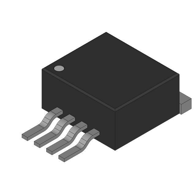
SANYO : SMP5
Specified sbstrate: 76.1×114.3×1.6mm3
Copper foil ratio 60% FR4
0
20
40
60
80
100
Ambient temperature, Ta - °C
120
140
160
MSG06072
Pin Assignment
(1) VIN (2) SWOUT
(3) GND
(4) VOS
(5) SS
No.A0490-2/5
�LA5774MP
Block Diagram
VIN 1
2 SWOUT
Reg.
OCP
Reset
OSC
Drive
Comp.
THD
4 VOS
Amp.
VREF
5
3
SS
GND
Application Circuit Example
L1
68μH
VIN
SWOUT
LA5774MP
C2
390μF
D1
SBD
C1
470μF
/50V
VOS
SS
GND
R2
R1
C3
1μF
Notes: C3 is for the soft start function. Delete C3 and keep the SS pin open when the soft start function is not necessary.
No.A0490-3/5
�LA5774MP
Description of Functional Settings
1. Calculation equation to set the output voltage
This IC controls the switching output so that the VOS pin voltage becomes 1.26V (typ).
The equation to set the output voltage is as follows:
R2
VO = 1+
× 1.26V(typ)
R1
The VOS pin has the inrush current of 1μA (typ). Therefore, the error becomes larger when R1 and R2 resistance
values are large.
2. Start delay function
The SS pin has the internally-connected 22μA (typ) constant-current supply. When the voltage of SS pin exceeds the
threshold voltage, the regulator starts operation. As the threshold voltage is 0.62V (typ), the start delay time can be
calculated as follows:
ex. For setting at 1μF
Td =
C × V 1μF × 0.62
=
= 28.2 ms
i
22μA
3. Soft start function
The internal PWM waveform has the voltage value as shown in the right.
If down-conversion from the voltage of VIN = 15 V to VIN = 3.3V is to be
made, for example, the PWM-ON duty has the value as shown below.
1.5V
0.62V
PWM wave
VOUT
PWMduty = V − Vsat + VF = 23 %
IN
(Note that calculation is made with Vsat = 1V and VF = 0.2V)
The output voltage of error amplifier, which is 3.3 V, is the value with PWM = 23%, as calculated in the above
equation, so that this voltage is determined as follows:
Ver = (ΔVPWM) × PWMduty + VPWML = 0.88V × 0.23 + 0.62V = 0.82V
(ΔVPWM is the PWM amplitude value or 0.88V(typ) while VPWML is the lower limit voltage of PWM
waveform or 0.62V(typ))
SS pin and error amplifier output voltages are designed to prefer the lower voltages, so that VOUT will reach the
designed regulation voltage in timing when the SS pin voltage exceeds the error amplifier output.
Therefore, the soft start time is calculated as follows:
Tss =
C × ΔVPWM × PWMduty C × 0.88 × PWMduty
=
22μA
i
For the set conditions of C = 1μF and PWMduty = 23%:
Tss =
1μF × 0.88V × 0.23
= 9.2ms
22μA
No.A0490-4/5
�LA5774MP
Timing Chart
VIN
SWOUT
VOUT
Td
Tss
ON Semiconductor and the ON logo are registered trademarks of Semiconductor Components Industries, LLC (SCILLC). SCILLC owns the rights to a number
of patents, trademarks, copyrights, trade secrets, and other intellectual property. A listing of SCILLC’s product/patent coverage may be accessed at
www.onsemi.com/site/pdf/Patent-Marking.pdf. SCILLC reserves the right to make changes without further notice to any products herein. SCILLC makes no
warranty, representation or guarantee regarding the suitability of its products for any particular purpose, nor does SCILLC assume any liability arising out of the
application or use of any product or circuit, and specifically disclaims any and all liability, including without limitation special, consequential or incidental
damages. “Typical” parameters which may be provided in SCILLC data sheets and/or specifications can and do vary in different applications and actual
performance may vary over time. All operating parameters, including “Typicals” must be validated for each customer application by customer’s technical
experts. SCILLC does not convey any license under its patent rights nor the rights of others. SCILLC products are not designed, intended, or authorized for use
as components in systems intended for surgical implant into the body, or other applications intended to support or sustain life, or for any other application in
which the failure of the SCILLC product could create a situation where personal injury or death may occur. Should Buyer purchase or use SCILLC products for
any such unintended or unauthorized application, Buyer shall indemnify and hold SCILLC and its officers, employees, subsidiaries, affiliates, and distributors
harmless against all claims, costs, damages, and expenses, and reasonable attorney fees arising out of, directly or indirectly, any claim of personal injury or
death associated with such unintended or unauthorized use, even if such claim alleges that SCILLC was negligent regarding the design or manufacture of the
part. SCILLC is an Equal Opportunity/Affirmative Action Employer. This literature is subject to all applicable copyright laws and is not for resale in any manner.
PS No.A0490-5/5
�


 工商网监
湘ICP备2023018690号
工商网监
湘ICP备2023018690号
