SPX2954
®
250mA Low Dropout Voltage Regulator
FEATURES
■ 5.0V and 3.3V Versions at 250mA
Output
■ Accurate 0.5% for SPX2954A
■ Very Low Quiescent Current
■ Low Dropout: 310mV at 250mA
■ Extremely Tight Load and Line Regulation
■ Very Low Temperature Coefficient
■ Current and Thermal Limiting
■ Need only 1µF for Stability
■ Direct Replacement for LP2954
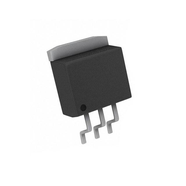
■ Offered in TO-92, TO-263, SOT-223, &
TO-220; also SOIC--8 Pin Versions Only
■ Error Flag Warns of Output Dropout
■ Logic-Controlled Electronic Shutdown
■ Programmable Output from 1.24V to 30V
+V IN
100K
8
ERROR
5
OUTPUT
+V IN
______
ERROR
V OUT
1.2 to 30V
1
SPX2954
SHUTDOWN
+
R1
3
SD
INPUT
3.3µF
.01µF
FB
GND
7
4
1.23V
V REF
R2
DESCRIPTION
The SPX2954 and SPX2954A are low power voltage regulators. These devices are an excellent
choice for use in battery-powered applications such as cordless telephones, radio control
systems, and portable computers. The SPX2954 and SPX2954A feature low quiescent current
and low dropout voltage (typ. 20mV at 100µA and 310mV at 250mA). This includes a tight initial
tolerance (0.5% for SPX2954A), extremely good load and line regulation (0.05% typ.), and very
low output temperature coefficient (20 ppm/°C typ.), making the SPX2954/SPX2954A useful as
a low-power voltage reference.
The error flag output feature is used as a power-on reset for warning of a low output voltage, due
to a falling input voltage. The logic-compatible shutdown feature enables the regulator to be
switched ON and OFF. The SPX2954/SPX2954A is offered in 3-pin TO-92, TO-263, SOT-223
and TO-220 packages, and 8 pin SOIC package.
Note:: Tab is internally connected to GND on T0-263, SOT-223, and TO-220-3.
TO-263-3 Package (T)
8-Pin Surface Mount (S)
TO-92 (N)
TO-263-5 Package (T5)
SPX2954
OUTPUT
1
SPX2954 SENSE
2
8
INPUT
7
FEEDBACK
6
5V, 3.3V TAP
1
2
SOT-223 Package (M3)
SPX2954
SPX2954
1
V IN
2
GND
3
1
3
1) INPUT
2SHUTDOWN
3 4 5
2) OUTPUT
GND 3) GND4
4) SHUTDOWN
5) ERROR
Top View
V OUT
Top View
1
2
3
SPX2954
SPX2954
1) INPUT
INPUT
OUTPUT
5
TO-220-3 Package (U) TO-220-5 Package (U5)
3
ERROR
GND
Bottom View
2) OUTPUT
VIN GND VOUT
3) GND
4) SHUTDOWN
5) ERROR
Front View
Top View
1 2 3
VIN GND VOUT
Front View
1 2 3 4 5
Front View
Pin Connections
Date: 12/9/05
SPX2954, 250mA Low Dropout Voltage Regulator
1
© Copyright 2005 Sipex Corporation
�ABSOLUTE MAXIMUM RATINGS
Power Dissipation........................................Internally Limited
Lead Temperature (soldering, 5 seconds) ................260°C
Storage Temperature Range........................-65°C to +150°C
Operating Junction Temperature Range......-40°C to +125°C
Input Supply Voltage...........................................-0.3V to +30V
ELECTRICAL CHARACTERISTICS
Feedback Input Voltage....................................-1.5V to +30V
Shutdown Input Voltage .................................-0.3V to +30V
Error Comparator Output...................................-0.3V to +30V
ESD Rating................................................................2kV Min
VIN =VO + 1V, IL=100µA, CL=1µF (NOTE 2), TA = 25°C, unless otherwise specified.
SPX2954A
PARAMETER
CONDITIONS
MIN.
SPX2954
TYP.
MAX
MIN. TYP. MAX.
UNIT
3.3 V Versions
Output Voltage
TJ=25°C
-25°C≤TJ≤85°C
Full Operating Temp.
3.284
3.267
3.260
3.3
3.3
3.3
3.317
3.333
3.340
3.267
3.251
3.234
3.3
3.3
3.3
3.333
3.350
3.366
V
Output Voltage
100µA ≤IL ≤250 mA
TJ ≤TJMAX
3.251
3.3
3.350
3.201
3.3
3.399
V
Output Voltage
TJ = 25°C
-25°C ≤TJ ≤85°C
Full Operating Temp.
4.975
4.950
4.940
5.0
5.0
5.0
5.025
5.050
5.060
4.950
4.925
4.900
5.0
5.0
5.0
5.050
5.075
5.100
V
Output Voltage
100µA ≤IL ≤250 mA
TJ ≤TJMAX
4.925
5.0
5.075
4.850
5.0
5.150
V
20
100
50
150
ppm/°C
Line Regulation (NOTE 3) VO+1V≤VIN≤30V |
(NOTE 4)
0.03
0.10
0.04
0.20
%
Load Regulation (NOTE 3) 100 µA≤IL≤250 mA
0.04
0.20
0.10
0.30
%
Dropout Voltage
(NOTE 5)
IL = 1mA
IL = 100 mA
IL = 250 mA
60
290
310
100
450
500
60
290
310
100
450
500
mV
Ground Current
IL = 1mA
IL = 100 mA
IL = 250 mA
150
3
10
170
6
14
150
3
10
170
6
14
µA
mA
mA
Current Limit
VOUT = 0
270
550
270
550
mA
0.05
0.2
0.05
0.2
%/W
5 V Versions
All Voltage Options
Output Voltage
Temperature Coefficient
(NOTE 1)
Thermal Regulation
Output Noise,
10Hz to 100kHz
CL = 1µF
430
430
µV rms
CL = 200 µF
CL = 3.3 µF, Bypass=
0.01µF from Pin 7 to
Pin 1 (8 pin Versions)
160
160
µV rms
100
100
µV rms
8-Pin Versions only
Reference Voltage
Reference Voltage
1.220
Over Temp (NOTE 6)
1.235
1.190
1.250
1.210 1.235 1.260
V
1.270
1.185
1.285
V
60
nA
Feedback Pin
Bias Current
40
Vref Temperature
Coefficient
20
50
ppm/°C
Feedback IBIAS
Temperature Coefficient
0.1
0.1
nA/°C
Date: 12/9/05
60
SPX2954, 250mA Low Dropout Voltage Regulator
2
40
© Copyright 2005 Sipex Corporation
�ELECTRICAL CHARACTERISTICS (Cont.)
VIN=VO+1V, IL=100µA, CL=1µF (NOTE 2), TA = 25°C, unless otherwise specified.
SPX2954A
PARAMETER
CONDITIONS
MIN. TYP.
SPX2954
MAX
MIN. TYP. MAX.
UNIT
0.01
1
0.01
1
µA
150
250
150
250
Error Comparator
Output Leakage Current
VOH = 30V
Output Low Voltage
VIN = VO-0.5V,
IOL = 400µA
Upper Threshold Voltage
(NOTE 7)
40
60
Lower Threshold Voltage
(NOTE 7)
75
Hysteresis
(NOTE 7)
15
40
95
60
75
mV
mV
95
15
mV
mV
Shutdown
Input logic Voltage
Shutdown Input Current
Low (Regulator ON)
High (Regulator OFF)
1.3
0.7
2.0
VS = 2.4V
VS= 30V
Regulator Output Current (NOTE 8)
in Shutdown
1.3
0.7
V
2.0
30
400
50
800
30
400
50
800
µA
3
10
3
10
µA
Thermal Resistance ΘJA
TO-263-3
31.4
°C/W
SOIC-8
128.4
°C/W
TO-92-3
131.9
°C/W
SOT-223
62.3
°C/W
TO-220-3
29.4
°C/W
NOTE 1: Output or reference voltage temperature coefficients defined as the worst case voltage change divided
by the total temperature range.
NOTE 2: Unless otherwise specified all limits guaranteed for TJ = 25°C, VIN = 6V, IL = 100µA and CL = 1µF.
Additional conditions for the 8-pin versions are feedback tied to 5V tap and output tied to output sense
(VOUT = 5V) and VSHUTDOWN ≤ 0.8V.
NOTE 3: Regulation is measured at constant junction temperature, using pulse testing with a low duty cycle.
Changes in output voltage due to heating effects are covered under the specification for thermal
regulation.
NOTE 4: Line regulation for the SPX2954 is tested at IL = 1mA.
NOTE 5: Dropout voltage is defined as the input to output differential at which the output voltage drops 100mV
below its nominal value measured at 1V differential. At very low values of programmed output voltage,
the minimum input supply voltage of 2V (2.3V over temperature) must be taken into account.
NOTE 6: VREF ≤VOUT ≤ (VIN - 1V), 2.3 ≤VIN≤30V, 100µA≤IL≤ 250mA, TJ ≤ TJMAX.
NOTE 7: Comparator thresholds are expressed in terms of a voltage differential at the feedback terminal below
the nominal reference voltage measured at 6V input. To express these thresholds in terms of output
voltage change, multiply by the error amplifier gain = VOUT/VREF = (R1 + R2)/R2. For example, at a
programmed output voltage of 5V, the error output is guaranteed to go low when the output drops by 95
mV x 5V/1.235 = 384 mV. Thresholds remain constant as a percent of VOUT as VOUT is varied, with the
dropout warning occurring at typically 5% below nominal, 7.5% guaranteed.
NOTE 8: VSHUTDOWN ≥ 2V, VIN ≤ 30V, VOUT =0, Feedback pin tied to 5V/3.3V Tap.
Date: 12/9/05
SPX2954, 250mA Low Dropout Voltage Regulator
3
© Copyright 2005 Sipex Corporation
�UNREGULATED DC
5V
8
1
INPUT
OUTPUT
7
+
FEEDBACK
2
SENSE
+
_
FROM
CMOS OR
TTL
3
180kΩ
6
ERROR
AMPLIFIER
330kΩ
5V TAP
SHUTDOWN
+
60kΩ
60 mV
+
______
+
_
+ 1.23V
1µF
.
5
ERROR
ERROR DETECTION
COMPARATOR
.
TO CMOS OR
TTL
4
REFERENCE
GROUND
SPX2954 Block Diagram, 8 Lead 5V Version
3.5
1.6
4
3.0
1.4
1.2
VOLTAGE NOISE
SPECTRAL DENSITY (µV/Hz)
5
OUTPUT VOLTAGE
CHANGE (mV)
1.8
2
0
-2
1.0
POWER
DISSIPATION (W)
SHUTDOWN THRESHOLD VOLTAGE (V)
TYPICAL PERFORMANCE CHARACTERISTICS
0.8
0.6
-75 -50 -25
0
25
50
~~
1
1.25W
C L = 220µF
2.0
1.0
10
20
30
40
50
10 2
TIME (µs)
Shutdown Threshold Voltage
C L = 3.3µF
C BYP = 0.1µF
1.5
0.0
-1
TEMPERATURE (ºC)
10 3
10 4
10 5
FREQUENCY (Hz), C BYP =0.1uF
Thermal Response
Output Noise
80
30
= 50µA
IL=50mA
25
20
70
I L = 100µA
15
T J = 150 ºC
10
5
RIPPLE REJECTION (dB)
OUTPUT VOLTAGE CHANGE (mV)
C L = 1µF
2.5
0.5
0
0
75 100 125 150
I L = 100mA
I L = 1mA
0
~~
10
5
0
T J = 125 ºC
I L = 100µA
60
I L = 100mA
50
40
C L = 1µF
V IN = 6V
V OUT = 5V
30
20
-5
10
-10
5
10
15
20
25
30
10 1
10 2
INPUT VOLTAGE (V)
Line Regulation
Date: 12/9/05
10 3
10 4
10 5
10 6
FREQUENCY (Hz)
Ripple Rejection
SPX2954, 250mA Low Dropout Voltage Regulator
4
© Copyright 2005 Sipex Corporation
�TYPICAL PERFORMANCE CHARACTERISTICS
6
10
250
225
R L =50kΩ
3
R L =50kΩ
2
R L = 50kΩ
175
150
125
100
RL =
8
4
GROUND PIN CURRENT (mA)
200
INPUT CURRENT (µA)
OUTPUT VOLTAGE (VOLTS)
5
75
50
1
1
0.1
25
0
0
2
3
4
5
0
6
1
2
320
240
INPUT CURRENT (mA)
GROUND CURRENT (µA)
280
I L = 1mA
200
160
IL= 0
120
80
40
1
2
3
5
6
7
8
4
5
0.01
0.1
9 10
6
7
8
100
6
R L =50 Ω
VOUT = 5V
5
V IN = 6V
I L = 100mA
4
3
0
1
2
3
4
5
6
7
8
-75 -50 -25
9 10
0
25 50
75 100 125 150
TEMPERATURE (ºC)
INPUT VOLTAGE (VOLTS)
Ground Current
10
Quiescent Current
160
150
140
130
120
110
100
90
80
70
60
50
40
30
20
10
0
INPUT VOLTAGE (VOLTS)
1
LOAD CURRENT (mA)
Input Current
Dropout Characteristics
0
4
INPUT VOLTAGE (VOLTS)
INPUT VOLTAGE (VOLTS)
0
3
GROUND CURRENT (mA)
1
0
Ground Current
Input Current
190
8
6
QUIESCENT CURRENT (µA)
GROUND CURRENT (mA)
7
I L =100mA
5
4
3
2
1
170
V IN =6V
I L =100uA
150
130
0
0
1
2
3
4
5
6
7
-75 -50 -25
8
Ground Current
Date: 12/9/05
0
25 50
75 100 125 150
TEMPERATURE (ºC)
INPUT VOLTAGE
Quiescent Current
SPX2954, 250mA Low Dropout Voltage Regulator
5
© Copyright 2005 Sipex Corporation
�TYPICAL PERFORMANCE CHARACTERISTICS (CONT.)
500
500
240
I L = 150mA
230
300
200
~
~
40
20
I L = 100µA
SHORT CIRCUIT CURRENT (mA)
400
DROP-OUT VOLTAGE (mV)
300
200
TJ = 25ºC
100
0
0
-75 -50 -25
0
25 50
100µA
75 100 125 150
1mA
TEMPERATURE (ºC)
10mA
210
200
190
180
170
-75 -50 -25
100mA
OUTPUT CURRENT
Drop-Out Voltage
2.5
T A = 125ºC
SINK CURRENT (mA)
HYSTERESIS
2
0
50
mV
1.5
T A = 25ºC
1.0
T A = -55ºC
0.5
0.0
1
0
2
3
4
5
0
8V
4V
0
0.0 0.1 0.2 0.3 0.4 0.5 0.6 0.7 0.8 0.9
INPUT VOLTAGE (V)
C L = 1µF
I L = 1mA
V OUT = 5V
-50
mV ~
~
6V
PULLUP RESISTOR TO
SEPARATE 5V SUPPLY
-2
200
OUTPUT LOW VOLTAGE (V)
Error Comparator Output
400
600
800
TIME(µs)
Comparator Sink Current
10
75 100 125 150
100
mV
2.0
4
25 50
Short Circuit Current
V OUT = 5V
6
0
TEMPERATURE (ºC)
Drop-Out Voltage
8
COMPARATOR OUTPUT (V)
220
INPUT OUTPUT VOLTAGE
VOLTAGE CHANGE
DROP-OUT VOLTAGE (mV)
400
Line Transient Response
90
90
80
80
70
70
I O = 100mA
1
0.5
V OUT = 5V
C L = 1µF
0.2
0.1
0.05
IL = 0
60
50
40
I L = 100µA
C L = 1µF
V IN = 6V
V OUT = 5V
30
0.02
RIPPLE REJECTION (dB)
I O = 1mA
2
RIPPLE REJECTION (dB)
OUTPUT IMPEDANCE (OHMS)
IO = 100µA
5
10
100
1K
10K
FREQUENCY (Hz)
Output Impedance
Date: 12/9/05
100K
1M
60
50
40
30
20
0.01
C L = 1µF
V IN = 6V
V OUT = 5V
I L = 1mA
I L = 10mA
20
10 1
10 2
10 3
10 4
10 5
10 6
FREQUENCY (Hz)
Ripple Rejection
10 1
10 2
10 3
10 4
10 5
10 6
FREQUENCY (Hz)
Ripple Rejection
SPX2954, 250mA Low Dropout Voltage Regulator
6
© Copyright 2005 Sipex Corporation
�TYPICAL PERFORMANCE CHARACTERISTICS (CONT.)
20
50
1.9
FEEDBACK CURRENT (µA)
2.1
0
-10
-20
-50 -25
0
25
50
-75 -50 -25
75 100 125 150
0
25 50
-2.0
6
150
40
20
50
0
-50
C L = 1µF
V OUT = 5V
100
mA
SHUTDOWN OUTPUT
PINOUT VOLTAGE (V) VOLTAGE (V)
7
60
100
0
-20
C L = 10µF
V OUT = 5V
-40
-60
~
~
100
µA
100
100
µA
µA
2
3
4
5
0
4
8
12
16
40
T A =25 ºC
T A = 85 ºC
5
10
15
20
INPUT VOLTAGE (V)
Maxium Rated Output
Date: 12/9/05
25
I L = 10mA
V IN = 8V
V OUT = 5V
1
C L = 10µF
0
2
0
0 100 200 300 400 500 600 700
Enable Transient
120
100
30
DIP SOLDERED
TO PC BOARD
T JMAX = 125º C
V OUT = 5V
300
200
100
80
60
T A = 25ºC
40
T A = 50ºC
20
0
0
0
2
TIME (us)
OUTPUT CURRENT (mA)
PIN 2 TO PIN 4 RESISTANCE (kΩ)
Vout=5V
20
3
8-PIN
MOLDED
T JMAX = 125 ºC
60
4
-100
400
80
1.0
5
20
Load Transient Response
TO-92 PACKAGE
0.25" LEADS SOLDERED
TO PC BOARD
100
0.5
C L = 1µF
TIME (ms)
120
0
-2
TIME (ms)
Load Transient Response
-0.5
-1.0
Feedback Pin Current
80
1
-1.5
FEEDBACK VOLTAGE (V)
200
0
T A = 55ºC
-200
250
~
~
T A = 25ºC
-150
75 100 125 150
Feedback Bias Current
LOAD OUTPUT VOLTAGE
CURRENT CHANGE (mV)
LOAD OUTPUT VOLTAGE
CURRENT CHANGE (mV)
Minimum Operating Voltage
-100
TA=1 25ºC
-100
TEMPEATURE (ºC)
TEMPERATURE
OUTPUT CURRENT (mA)
-50
-250
-30
1.7
-75
PIN 7 DRIVEN BY EXTERNAL
SOURCE (REGULATOR RUN
OPEN LOOP)
0
10
BIAS CURRENT (nA)
MINIMUM OPERATING VOLTAGE (V)
2.3
-75
T A = 85ºC
0
-50 -25
0
25
50
75 100 125 150
TEMPERATURE (ºC)
Divider Resistance
0
5
10
15
20
25
30
INPUT VOLTAGE (V)
Maxium Rated Output Current
SPX2954, 250mA Low Dropout Voltage Regulator
7
© Copyright 2005 Sipex Corporation
�APPLICATIONS HINTS
EXTERNAL CAPACITORS
ERROR DETECTION COMPARATOR
OUTPUT
The stability of the SPX2954 requires a 1µF or
greater capacitor between output and ground.
Oscillation could occur without this capacitor.
Most types of tantalum or aluminum electrolytic works fine here. For operations below
-25°C solid tantalum is recommended since the
many aluminum types have electrolytes that
freeze at about -30°C. The ESR of about 5Ω or
less and resonant frequency above 500kHz are
the most important parameters in the value of
the capacitor. The capacitors value may be increased without limit.
The comparator produces a logic low output
whenever the SPX2954 output falls out of regulation by more than around 5%. This is around
60 mV offset divided by the 1.235 reference
voltage. This trip level remains 5% below normal regardless of the programmed output voltage of the regulator.
Figure 1 shows the timing diagram depicting the
ERROR signal and the regulator output voltage
as the SPX2954 input is ramped up and down.
The ERROR signal becomes low at around 1.3V
input, and goes high around 5V input (input
voltage at which VOUT = 4.75). Since the
SPX2954’s dropout voltage is load dependent,
the input voltage trip point (around 5V) will
vary with the load current. The output voltage
trip point (approx. 4.75V) does not vary with
load.
At lower values of output current, less output
capacitance is required for stability. For the
currents below 10mA the value of the capacitor
can be reduced to 0.33µF and 0.1µF for 1mA.
More output capacitance is needed for the 8-pin
version at voltages below 5V since it runs the
error amplifier at lower gain. At worst case 3.3
µF or greater must be used for the condition of
150mA load at 1.23V output.
The error comparator has an open-collector output, which requires an external pull-up resistor.
Depending on the system requirements the resistor may be returned to 5V output or other
supply voltage. In determining the value of this
resistor, note that the output is rated to sink
400mA, this value adds to battery drain in a low
battery condition. Suggested values range from
100k to 1MΩ. If the output is unused this resistor is not required.
The SPX2954 unlike other low dropout regulators will remain stable and in regulation with no
load in addition to the internal voltage divider.
This feature is especially important in applications like CMOS RAM keep-alive. When setting the output voltage of the SPX2954 version
with external resistors, a minimum load of 1µA
is recommended
If there is more than 10 inches of wire between
the input and the AC filter capacitor or if a
battery is used as the input then a 1µF tantalum
or aluminum electrolytic capacitor should be
placed from the input to the ground.
PROGRAMMING
THE
VOLTAGE OF SPX2954
OUTPUT
The SPX2954 may be pin-strapped for 5V using
its internal voltage divider by tying Pin 1 (output) to Pin 2 (sense) and Pin 7 (feedback) to Pin
6 (5V Tap). Also, it may be programmed for any
output voltage between its 1.235V reference
and its 30V maximum rating using an external
pair of resistors. Refer to the below equation for
the programming of the output voltage:
Instability can occur if there is stray capacitance
to the SPX2954 feedback terminal (pin 7). This
could cause more problems when using a higher
value of external resistors to set the output
voltage. This problem can be fixed by adding a
100pF capacitor between output and feedback
and increasing the output capacitor to at least
3.3µF.
VOUT = VREF x (1 + R1/R2)+ IFBR1
The VREF is 1.235 and IFB is the feedback bias
current, nominally -20nA. The minimum
recommended load current of 1 µA forces an
Date: 12/9/05
SPX2954, 250mA Low Dropout Voltage Regulator
8
© Copyright 2005 Sipex Corporation
�APPLICATIONS HINTS (CONT)
+V IN
upper limit of 1.2MΩ on value of R2. If no load
is presented the IFB produces an error of typically
2% in VOUT which may be eliminated at room
temperature by trimming R1. To improve the
accuracy choose the value of R2 = 100k this
reduces the error by 0.17% and increases the
resistor program current by 12µA. Since the
SPX2954 typically draws 60µA at no load with
Pin 2 open-circuited, this is a small price to pay.
470KΩ
8
+V IN
______
ERROR
5
V OUT
470kΩ
V OUT
1
SPX2954
+
3
R1
SD
RESET
GND
FB
4
7
REDUCING OUTPUT NOISE
1µF
R2
It may be an advantage to reduce the AC noise
present at the output. One way is to reduce the
regulator bandwidth by increasing the size of the
output capacitor. This is the only way that noise
can be reduced on the 3 lead SPX2954 but is
relatively inefficient, as increasing the capacitor
from 1µF to 220 µF only decreases the noise
from 430µV to 160µVRMS for a 100kHz bandwidth at 5V output. Noise can be reduced fourfold by using a bypass capacitor across R1, since
it reduces the high frequency gain from 4 to
unity. Pick
Figure 2. Latch Off when Error Flag Occurs
+V IN
8
ERROR
5
OUTPUT
+V IN
______
ERROR
1
V OUT
*V OUT = V IN
SPX2954
SHUTDOWN
INPUT
CBYPASS ≅ (1 / 2πR1 x 200 Hz)
3
SD
GND
4
or choose 0.01µF. When doing this, the output
capacitor must be increased to 3.3µF to maintain
stability. These changes reduce the output noise
from 430µV to 100µVRMS for a 100kHz bandwidth at 5V output. With the bypass capacitor
added, noise no longer scales with output voltage so that improvements are more dramatic at
higher output voltages.
FB
7
*MINIMUM INPUT-OUTPUT VOLTAGE RANGES FROM 40mV to 400mV.
DEPENDING ON LOAD CURRENT.
Figure 3. Wide Imput Voltage Range, Current Limiter
4.75V
OUTPUT
VOLTAGE
_______
ERROR*
+5.0V
INPUT
VOLTAGE
+1.3V
+
+
* See Application Info.
Figure 1. Error Output Timing
Date: 12/9/05
SPX2954, 250mA Low Dropout Voltage Regulator
9
© Copyright 2005 Sipex Corporation
�APPLICATIONS HINTS
+
6V
SEALED
LEADACID
BATTERY
SOURCE
1.5kΩ
120kΩ
8
1N457
+V IN
FB
SPX385
V OUT
1
MAIN V+
SPX2954
FOR 5.5 V
MEMORY V+
SENSE
400kΩ
2
3
+
1µF
SD
100kΩ
20kΩ
GND
NI-CAD
BACKUP
BATTERY
4
Figure 4. Low Battery Disconnect
8
39kΩ
5
2
SENS E
+V IN
______
ERROR
1
+VO UT = 5V
VOUT
RESET
+
1uF
SPX2954
-
3
SD
C4
+
7
FB
39kΩ
1%
TAP
GND
4
6
100kΩ
100kΩ
C1
+
6V
LEADACID
BATTERY
1kΩ


 工商网监
湘ICP备2023018690号
工商网监
湘ICP备2023018690号
