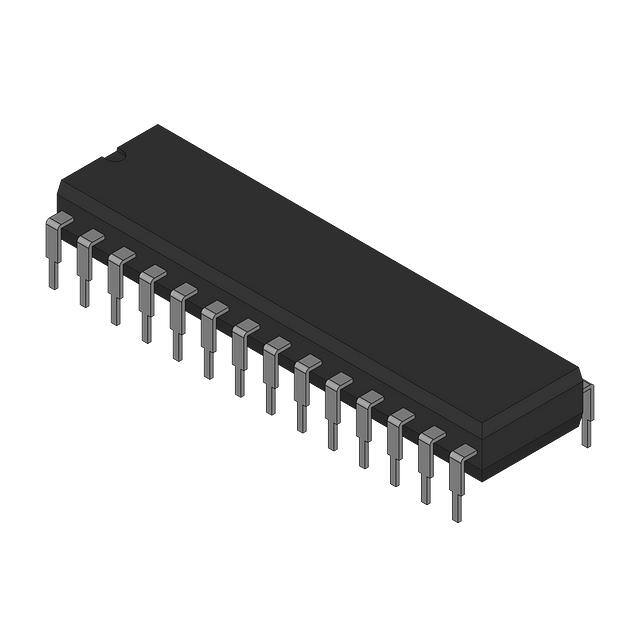
FM1808B (PDIP)
256Kb Bytewide 5V F-RAM Memory
Features
256Kbit Ferroelectric Nonvolatile RAM
Organized as 32,768 x 8 bits
High Endurance 1 Trillion (1012) Read/Writes
38 year Data Retention @ +75 C
NoDelay™ Writes
Advanced High-Reliability Ferroelectric Process
Superior to BBSRAM Modules
No Battery Concerns
Monolithic Reliability
Superior for Moisture, Shock, and Vibration
Resistant to Negative Voltage Undershoots
SRAM & EEPROM Compatible
JEDEC 32Kx8 SRAM & EEPROM pinout
70 ns Access Time
130 ns Cycle Time
Low Power Operation
15 mA Active Current
25 A (typ.) Standby Current
Industry Standard Configuration
Extended Temperature 0 C to +85 C
28-pin “Green”/RoHS PDIP Package
Description
Pin Configuration
The FM1808B is a 256-kilobit nonvolatile memory
employing an advanced ferroelectric process. A
ferroelectric random access memory or F-RAM is
nonvolatile but operates in other respects as a RAM.
It provides data retention for 38 years while
eliminating the reliability concerns, functional
disadvantages and system design complexities of
battery-backed SRAM (BBSRAM). Fast write timing
and high write endurance make F-RAM superior to
other types of nonvolatile memory.
In-system operation of the FM1808B is very similar
to other RAM devices. Minimum read- and writecycle times are equal. The F-RAM memory, however,
is nonvolatile due to its unique ferroelectric memory
process. Unlike BBSRAM, the FM1808B is a truly
monolithic nonvolatile memory. It provides the same
functional benefits of a fast write without the
disadvantages associated with modules and batteries
or hybrid memory solutions.
These capabilities make the FM1808B ideal for
nonvolatile memory applications requiring frequent
or rapid writes in a bytewide environment. The
availability of a through-hole package allows ease of
insertion and removal in systems that utilize a DIP
socket. Device specifications are guaranteed over a
extended temperature range of 0°C to +85°C.
A14
1
28
VDD
A12
2
27
WE
A7
3
26
A13
A6
4
25
A8
A5
5
24
A9
A4
6
23
A11
A3
7
22
OE
A2
8
21
A10
A1
9
20
CE
A0
10
19
DQ7
DQ0
11
18
DQ6
DQ1
12
17
DQ5
DQ2
13
16
DQ4
VSS
14
15
DQ3
Ordering Information
FM1808B-PG
28-pin “Green”/RoHS PDIP
This product conforms to specifications per the terms of the Ramtron standard warranty. The product has completed Ramtron’s
internal qualification testing and has reached production status.
Cypress Semiconductor Corporation
•
Document Number: 001-86600 Rev. **
198 Champion Court
•
San Jose, CA 95134-1709 • 408-943-2600
Revised March 19, 2013
�FM1808B (PDIP)
A0-A14
Address
Latch &
Decoder
A0-A14
32,768 x 8 FRAM Array
CE
Control
Logic
WE
I/O Latch
Bus Driver
OE
DQ0-7
Figure 1. Block Diagram
Pin Description
Pin Name
A(14:0)
Type
Input
DQ(7:0)
/CE
I/O
Input
/OE
Input
/WE
Input
VDD
VSS
Supply
Supply
Functional Truth Table
/CE
/WE
H
X
X
L
H
L
Description
Address: The 15 address lines select one of 32,768 bytes in the F-RAM array. The
address value is latched on the falling edge of /CE.
Data: 8-bit bi-directional data bus for accessing the F-RAM array.
Chip Enable: /CE selects the device when low. Asserting /CE low causes the
address to be latched internally. Address changes that occur after /CE goes low
will be ignored until the next falling edge occurs.
Output Enable: Asserting /OE low causes the FM1808B to drive the data bus when
valid data is available. Deasserting /OE high causes the DQ pins to be tri-stated.
Write Enable: Asserting /WE low causes the FM1808B to write the contents of the
data bus to the address location latched by the falling edge of /CE.
Supply Voltage: 5V
Ground
Function
Standby/Precharge
Latch Address (and Begin Write if /WE=low)
Read
Write
Note: The /OE pin controls only the DQ output buffers.
Document Number: 001-86600 Rev. **
Page 2 of 12
�FM1808B (PDIP)
Overview
The FM1808B is a bytewide F-RAM memory. The
memory array is logically organized as 32,768 x 8
and is accessed using an industry standard parallel
interface. All data written to the part is immediately
nonvolatile with no delay. Functional operation of the
F-RAM memory is the same as SRAM type devices,
except the FM1808B requires a falling edge of /CE to
start each memory cycle.
Memory Architecture
Users access 32,768 memory locations each with 8
data bits through a parallel interface. The complete
15-bit address specifies each of the 32,768 bytes
uniquely. Internally, the memory array is organized
into 4096 rows of 8-bytes each. This row
segmentation has no effect on operation, however the
user may wish to group data into blocks by its
endurance characteristics as explained on page 4.
memory cycle must be completed internally even if
/CE goes inactive. Data becomes available on the bus
after the access time has been satisfied.
After the address has been latched, the address value
may be changed upon satisfying the hold time
parameter. Unlike an SRAM, changing address values
will have no effect on the memory operation after the
address is latched.
The FM1808B will drive the data bus when /OE is
asserted low. If /OE is asserted after the memory
access time has been satisfied, the data bus will be
driven with valid data. If /OE is asserted prior to
completion of the memory access, the data bus will
not be driven until valid data is available. This feature
minimizes supply current in the system by eliminating
transients caused by invalid data being driven onto
the bus. When /OE is inactive the data bus will
remain tri-stated.
The cycle time is the same for read and write memory
operations. This simplifies memory controller logic
and timing circuits. Likewise the access time is the
same for read and write memory operations. When
/CE is deasserted high, a precharge operation begins,
and is required of every memory cycle. Thus unlike
SRAM, the access and cycle times are not equal.
Writes occur immediately at the end of the access
with no delay. Unlike an EEPROM, it is not
necessary to poll the device for a ready condition
since writes occur at bus speed.
Write Operation
Writes occur in the FM1808B in the same time
interval as reads. The FM1808B supports both /CEand /WE-controlled write cycles. In all cases, the
address is latched on the falling edge of /CE.
It is the user’s responsibility to ensure that VDD
remains within datasheet tolerances to prevent
incorrect operation. Also proper voltage level and
timing relationships between VDD and /CE must be
maintained during power-up and power-down events.
See Power Cycle Timing diagram on page 9.
In a /WE controlled write, the memory cycle begins
on the falling edge of /CE. The /WE signal falls after
the falling edge of /CE. Therefore, the memory cycle
begins as a read. The data bus will be driven
according to the state of /OE until /WE falls. The
timing of both /CE- and /WE-controlled write cycles
is shown in the electrical specifications.
Memory Operation
The FM1808B is designed to operate in a manner
similar to other bytewide memory products. For users
familiar with BBSRAM, the performance is
comparable but the bytewide interface operates in a
slightly different manner as described below. For
users familiar with EEPROM, the obvious differences
result from the higher write performance of F-RAM
technology including NoDelay writes and much
higher write endurance.
Read Operation
A read operation begins on the falling edge of /CE.
At this time, the address bits are latched and a
memory cycle is initiated. Once started, a full
Document Number: 001-86600 Rev. **
In a /CE controlled write, the /WE signal is asserted
prior to beginning the memory cycle. That is, /WE is
low when /CE falls. In this case, the part begins the
memory cycle as a write. The FM1808B will not
drive the data bus regardless of the state of /OE.
Write access to the array begins asynchronously after
the memory cycle is initiated. The write access
terminates on the rising edge of /WE or /CE,
whichever is first. Data set-up time, as shown in the
electrical specifications, indicates the interval during
which data cannot change prior to the end of the write
access.
Unlike other truly nonvolatile memory technologies,
there is no write delay with F-RAM. Since the read
and write access times of the underlying memory are
the same, the user experiences no delay through the
bus. The entire memory operation occurs in a single
bus cycle. Therefore, any operation including read or
write can occur immediately following a write. Data
Page 3 of 12
�FM1808B (PDIP)
polling, a technique used with EEPROMs to
determine if a write is complete, is unnecessary.
accesses per second to the same row for over 10
years.
Precharge Operation
The precharge operation is an internal condition that
prepares the memory for a new access. All memory
cycles consist of a memory access and a precharge.
The precharge is initiated by deasserting the /CE pin
high. It must remain high for at least the minimum
precharge time tPC.
F-RAM Design Considerations
When designing with F-RAM for the first time, users
of SRAM will recognize a few minor differences.
First, bytewide F-RAM memories latch each address
on the falling edge of chip enable. This allows the
address bus to change after starting the memory
access. Since every access latches the memory
address on the falling edge of /CE, users cannot
ground it as they might with SRAM.
The user determines the beginning of this operation
since a precharge will not begin until /CE rises.
However, the device has a maximum /CE low time
specification that must be satisfied.
Users who are modifying existing designs to use FRAM should examine the memory controller for
timing compatibility of address and control pins.
Each memory access must be qualified with a low
transition of /CE. In many cases, this is the only
change required. An example of the signal
relationships is shown in Figure 2 below. Also shown
is a common SRAM signal relationship that will not
work for the FM1808B.
Endurance
Internally, a F-RAM operates with a read and restore
mechanism. Therefore, each read and write cycle
involves a change of state. The memory architecture
is based on an array of rows and columns. Each read
or write access causes an endurance cycle for an
entire row. In the FM1808B, a row is 64 bits wide.
Every 8-byte boundary marks the beginning of a new
row. Endurance can be optimized by ensuring
frequently accessed data is located in different rows.
Regardless, F-RAM offers substantially higher write
endurance than other nonvolatile memories. The
rated endurance limit of 1012 cycles will allow 3,000
The reason for /CE to strobe for each address is twofold: it latches the new address and creates the
necessary precharge period while /CE is high.
Valid Strobing of /CE
CE
FRAM
Signaling
Address
A1
A2
Data
D1
D2
Invalid Strobing of /CE
CE
SRAM
Signaling
Address
Data
A1
A2
D1
D2
Figure 2. Chip Enable and Memory Address Relationships
Document Number: 001-86600 Rev. **
Page 4 of 12
�FM1808B (PDIP)
A second design consideration relates to the level of
VDD during operation. Battery-backed SRAMs are
forced to monitor VDD in order to switch to battery
backup. They typically block user access below a
certain VDD level in order to prevent loading the
battery with current demand from an active SRAM.
The user can be abruptly cut off from access to the
nonvolatile memory in a power down situation with
no warning or indication.
below VDD min. (4.5V). Figure 3 shows a pullup
resistor on /CE which will keep the pin high during
power cycles assuming the MCU/MPU pin tri-states
during the reset condition. The pullup resistor value
should be chosen to ensure the /CE pin tracks VDD yet
a high enough value that the current drawn when /CE
is low is not an issue.
F-RAM memories do not need this system overhead.
The memory will not block access at any VDD level
that complies with the specified operating range. The
user should take measures to prevent the processor
from accessing memory when VDD is out-oftolerance. The common design practice of holding a
processor in reset during powerdown may be
sufficient. It is recommended that Chip Enable is
pulled high and allowed to track VDD during powerup
and powerdown cycles. It is the user’s responsibility
to ensure that chip enable is high to prevent accesses
R
Document Number: 001-86600 Rev. **
VDD
FM1808B
CE
MCU/
MPU
WE
OE
A(14:0)
DQ
Figure 3. Use of Pullup Resistor on /CE
Page 5 of 12
�FM1808B (PDIP)
Electrical Specifications
Absolute Maximum Ratings
Symbol
Description
VDD
Power Supply Voltage with respect to VSS
VIN
Voltage on any pin with respect to VSS
TSTG
TLEAD
VESD
Storage Temperature
Lead Temperature (Soldering, 10 seconds)
Electrostatic Discharge Voltage
- Human Body Model (AEC-Q100-002 Rev. E)
- Charged Device Model (AEC-Q100-011 Rev. B)
- Machine Model (AEC-Q100-003 Rev. E)
Ratings
-1.0V to +7.0V
-1.0V to +7.0V
and VIN < VDD+1.0V
-55 C to + 125 C
260 C
4kV
1.25kV
300V
Stresses above those listed under Absolute Maximum Ratings may cause permanent damage to the device. This is a stress rating
only, and the functional operation of the device at these or any other conditions above those listed in the operational section of this
specification is not implied. Exposure to absolute maximum ratings conditions for extended periods may affect device reliability.
DC Operating Conditions (TA = 0 C to + 85 C, VDD = 4.5V to 5.5V unless otherwise specified)
Symbol Parameter
Min
Typ
Max
VDD
Power Supply
4.5
5.0
5.5
IDD
VDD Supply Current
15
ISB1
Standby Current (TTL)
1.8
ISB2
Standby Current (CMOS)
25
50
ILI
Input Leakage Current
1
ILO
Output Leakage Current
1
VIH
Input High Voltage
2.0
VDD+0.3
VIL
Input Low Voltage
-0.3
0.8
VOH1
Output High Voltage (IOH = -2 mA)
2.4
VOH2
Output High Voltage (IOH = -100 A)
VDD-0.2
VOL1
Output Low Voltage (IOL = 4.2 mA)
0.4
VOL2
Output Low Voltage (IOL = 150 A)
0.2
Units
V
mA
mA
A
A
A
V
V
V
V
V
V
Notes
1
2
3
4
4
Notes
1. VDD = 5.5V, /CE cycling at minimum cycle time. All inputs at CMOS levels, all outputs unloaded.
2. VDD = 5.5V, /CE at VIH, All other pins at TTL levels.
3. VDD = 5.5V, /CE at VIH, All other pins at CMOS levels (0.2V or VDD-0.2V).
4. VIN, VOUT between VDD and VSS.
Document Number: 001-86600 Rev. **
Page 6 of 12
�FM1808B (PDIP)
Read Cycle AC Parameters (TA = 0 C to + 85 C, VDD = 4.5V to 5.5V unless otherwise specified)
Symbol
Parameter
Min
Max
Units
tCE
Chip Enable Access Time (to data valid)
70
ns
tCA
Chip Enable Active Time
70
ns
tRC
Read Cycle Time
130
ns
tPC
Precharge Time
60
ns
tAS
Address Setup Time
0
ns
tAH
Address Hold Time
15
ns
tOE
Output Enable Access Time
12
ns
tHZ
Chip Enable to Output High-Z
15
ns
tOHZ
Output Enable to Output High-Z
15
ns
Notes
1
1
Write Cycle AC Parameters (TA = 0 C to + 85 C, VDD = 4.5V to 5.5V unless otherwise specified)
Symbol
Parameter
Min
Max
Units
tCA
Chip Enable Active Time
70
ns
tCW
Chip Enable to Write High
70
ns
tWC
Write Cycle Time
130
ns
tPC
Precharge Time
60
ns
tAS
Address Setup Time
0
ns
tAH
Address Hold Time
15
ns
tWP
Write Enable Pulse Width
40
ns
tDS
Data Setup
30
ns
tDH
Data Hold
0
ns
tWZ
Write Enable Low to Output High Z
15
ns
tWX
Write Enable High to Output Driven
10
ns
tHZ
Chip Enable to Output High-Z
15
ns
tWS
Write Enable Setup
0
ns
tWH
Write Enable Hold
0
ns
Notes
1
1
1
2
2
Notes
1
This parameter is periodically sampled and not 100% tested.
2
The relationship between /CE and /WE determines if a /CE- or /WE-controlled write occurs. There is no timing
specification associated with this relationship.
Data Retention (TA = 0 C to + 85 C)
Symbol
Parameter
TDR
@ +85ºC
@ +80ºC
@ +75ºC
Capacitance (TA = 25 C, f=1.0 MHz, VDD = 5V)
Symbol
Parameter
CI/O
Input/Output Capacitance (DQ)
CIN
Input Capacitance
Document Number: 001-86600 Rev. **
Min
10
19
38
Min
-
Max
8
6
Max
-
Units
pF
pF
Units
Years
Years
Years
Notes
Notes
Page 7 of 12
�FM1808B (PDIP)
AC Test Conditions
Input Pulse Levels
Input rise and fall times
Input and output timing levels
Equivalent AC Load Circuit
0 to 3V
10 ns
1.5V
Read Cycle Timing
tRC
tCA
tPC
CE
tAH
tAS
A(14:0)
tOE
OE
tOHZ
DQ(7:0)
tCE
tHZ
Write Cycle Timing - /CE Controlled Timing
tWC
tCA
tPC
CE
tAS
tAH
A(14:0)
tWS
tWH
WE
OE
tDS
tDH
DQ(7:0)
Document Number: 001-86600 Rev. **
Page 8 of 12
�FM1808B (PDIP)
Write Cycle Timing - /WE Controlled Timing
tWC
tCA
tPC
tC W
CE
tAS
tAH
A(14:0)
tWH
tWS
tWP
WE
OE
tWZ
tWX
DQ(7:0)
out
tDS
tDH
DQ(7:0)
in
Power Cycle Timing
VDD (min)
VDD
VDD (min)
t PD
t PU
t PC
CE
VIH (min)
VIH (min)
VIL (max)
Power Cycle Timing (TA = 0 C to + 85 C, VDD = 4.5V to 5.5V unless otherwise specified)
Symbol
Parameter
Min
Max
Units
tPU
VDD(min) to First Access Start
10
ms
tPD
Last Access Complete to VDD(min)
0
s
tVR
VDD Rise Time
30
s/V
tVF
VDD Fall Time
30
s/V
Notes
2
1,2
1,2
Notes
1
Slope measured at any point on VDD waveform.
2
This parameter has been characterized and not 100% tested at 0°C.
Document Number: 001-86600 Rev. **
Page 9 of 12
�FM1808B (PDIP)
28-pin DIP (JEDEC MS-011)
All dimensions in inches
0.485
0.580
PIN 1
1.380
1.565
0.015
min.
0.005
min.
0.600
0.625
0.125
0.195
0.250 max
0.100 BSC
0.030
0.070
0.014
0.022
0.115
0.200
0.600 BSC
0.700 max.
DIP Package Marking Scheme
RAMTRON
XXXXXXX-PT
RYYWWLLLLLLL
Legend:
XXXXXX= part number, P= package (PG=PDIP “Green”),
T=temp. range (=extended, C=commercial),
R=rev code, YY=year, WW=work week, LLLLLL= lot code
Example: FM1808B, “Green”/RoHS PDIP package,
A die rev., Year 2010, Work Week 49, Lot code L3502G1
RAMTRON
FM1808B-PG
A1049L3502G1
Document Number: 001-86600 Rev. **
Page 10 of 12
�FM1808B (PDIP)
Revision History
Revision
1.0
1.1
Date
12/29/2010
2/22/2011
1.2
3/10/2011
2.0
1/6/2012
Summary
Initial Release
Changed to commercial temp range. Changed tPU and tVF spec limits. Updated
package marking.
Changed operating temperature to 0C to +85C. Removed “C” from part
marking. Added more temperature entries in data retention table.
Changed to Pre-Production status. Changed tVF spec.
Document History
Document Title: FM1808B (PDIP) 256Kb Bytewide 5V F-RAM Memory
Document Number: 001-86600
Revision
ECN
Orig. of
Change
Submissio
n Date
**
3930341
GVCH
03/19/2013
Document Number: 001-86600 Rev. **
Description of Change
New Spec
Page 11 of 12
�FM1808B (PDIP)
Sales, Solutions, and Legal Information
Worldwide Sales and Design Support
Cypress maintains a worldwide network of offices, solution centers, manufacturer’s representatives, and distributors.
To find the office closest to you, visit us at Cypress Locations.
PSoC® Solutions
Products
Automotive
cypress.com/go/automotive
psoc.cypress.com/solutions
Clocks & Buffers
cypress.com/go/clocks
PSoC 1 | PSoC 3 | PSoC 5
Interface
cypress.com/go/interface
Lighting & Power Control
cypress.com/go/powerpsoc
cypress.com/go/plc
Memory
cypress.com/go/memory
PSoC
cypress.com/go/psoc
Touch Sensing
cypress.com/go/touch
USB Controllers
cypress.com/go/usb
Cypress Developer Community
Community | Forums | Blogs | Video | Training
Technical Support
cypress.com/go/support
RAMTRON is a registered trademark and NoDelay™ is a trademark of Cypress Semiconductor Corp. All other trademarks or registered
trademarks referenced herein are the property of their respective owners.
© Cypress Semiconductor Corporation, 2011-2013. The information contained herein is subject to change without notice. Cypress
Semiconductor Corporation assumes no responsibility for the use of any circuitry other than circuitry embodied in a Cypress product. Nor
does it convey or imply any license under patent or other rights. Cypress products are not warranted nor intended to be used for medical,
life support, life saving, critical control or safety applications, unless pursuant to an express written agreement with Cypress. Furthermore,
Cypress does not authorize its products for use as critical components in life-support systems where a malfunction or failure may
reasonably be expected to result in significant injury to the user. The inclusion of Cypress products in life-support systems application
implies that the manufacturer assumes all risk of such use and in doing so indemnifies Cypress against all charges.
This Source Code (software and/or firmware) is owned by Cypress Semiconductor Corporation (Cypress) and is protected by and subject to
worldwide patent protection (United States and foreign), United States copyright laws and international treaty provisions. Cypress hereby
grants to licensee a personal, non-exclusive, non-transferable license to copy, use, modify, create derivative works of, and compile the
Cypress Source Code and derivative works for the sole purpose of creating custom software and or firmware in support of licensee product
to be used only in conjunction with a Cypress integrated circuit as specified in the applicable agreement. Any reproduction, modification,
translation, compilation, or representation of this Source Code except as specified above is prohibited without the express written
permission of Cypress.
Disclaimer: CYPRESS MAKES NO WARRANTY OF ANY KIND, EXPRESS OR IMPLIED, WITH REGARD TO THIS MATERIAL,
INCLUDING, BUT NOT LIMITED TO, THE IMPLIED WARRANTIES OF MERCHANTABILITY AND FITNESS FOR A PARTICULAR
PURPOSE. Cypress reserves the right to make changes without further notice to the materials described herein. Cypress does not assume
any liability arising out of the application or use of any product or circuit described herein. Cypress does not authorize its products for use
as critical components in life-support systems where a malfunction or failure may reasonably be expected to result in significant injury to
the user. The inclusion of Cypress’ product in a life-support systems application implies that the manufacturer assumes all risk of such use
and in doing so indemnifies Cypress against all charges.
Use may be limited by and subject to the applicable Cypress software license agreement.
Document Number: 001-86600 Rev. **
Page 12 of 12
�


 工商网监
湘ICP备2023018690号
工商网监
湘ICP备2023018690号
