MUSES8920
High Quality Audio J-FET Input
Dual Operational Amplifier
■ GENERAL DESCRIPTION
The MUSES8920 is a high quality audio J-FET input dual operational
amplifier, which is optimized for high-end audio, professional audio and
portable audio applications.
It is suitable for audio preamplifiers, active filters, and line amplifiers.
In addition, J-FET input type has advantage of the low input bias current,
it is suitable for transimpedance amplifier (I/V converter).
■ FEATURES
●Operating Voltage
●Low Noise
●THD
●Slew Rate
●GBW
●High Output Current
●J-FET Input
●Bipolar Technology
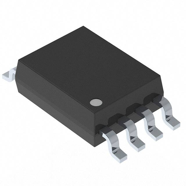
●Package Outline
■ PACKAGE OUTLINE
MUSES8920D
(DIP8)
MUSES8920E
(SOP8 JEDEC 150mil (EMP8))
MUSES8920KX7
(DFN8-X7 (ESON8-X7))
±3.5V to ±17V
8nV/√Hz typ.
0.0004% typ. (Av=1)
25V/µs typ.
11MHz typ.
100mA typ.(short-circuit current)
■ PIN CONFIGLATION
DIP8, SOP8 JEDEC 150mil
1
2
7
A
3
DIP8, SOP8 JEDEC 150mil
DFN8-X7 (ESON8-X7)(3.5mm x 4.0mm)
1. A OUTPUT
2. A -INPUT
3. A +INPUT
4. V5. B +INPUT
6. B -INPUT
7. B OUTPUT
8.V+
8
B
4
6
5
DFN8-X7 (ESON8-X7)
Bottom View
Top View
■ APPLICATIONS
● Portable Audio
● Home Audio
● Professional Audio
● Car Audio
1
2
3
4
A
B
8
8
1
7
7
2
6
6
5
5
Exposed
Pad
3
4
About Exposed Pad
Connect the Exposed Pad on the GND.
I/V
Digital
Input
DA
Converter
Analog
Output
I/V
LPF
Buff
DAC Output I/V converter + LPF circuit
MUSES and this logo are trademarks of New Japan Radio Co., Ltd.
Ver.10
-1-
�MUSES8920
■ ABSOLUTE MAXIMUM RATING (Ta=25ºC unless otherwise specified)
PARAMETER
Supply Voltage
Differential Input Voltage Range
Common Mode Input Voltage Range
Power Dissipation
Operating Temperature Range
Storage Temperature Range
SYMBOL
RATING
UNIT
V /V
±18
V
VID
±30
V
+
-
(Note1)
VICM
±15
DIP8:870
SOP8:900 (Note2)
DFN8-X7: 690 (Note2)
2900 (Note3)
-40 to +125
-50 to +150
PD
Topr
Tstg
V
mW
ºC
ºC
(Note1) For supply Voltages less than ±15 V, the maximum input voltage is equal to the Supply Voltage.
(Note2) Mounted on the EIA/JEDEC standard board (114.3×76.2×1.6mm, two layer, FR-4). DFN8 is connecting to GND in the center part on the back.
(Note3) EIA/JEDEC STANDARD Test board (76.2 x 114.3 x 1.6mm, 4layers, FR-4, Applying a thermal via hole to a board based on JEDEC standard JESD51-5)
mounting. The PAD connecting to GND in the center part on the back.
(Note4) NJM8920 is ESD (electrostatic discharge) sensitive device.
Therefore, proper ESD precautions are recommended to avoid permanent damage or loss of functionality.
■ RECOMMENDED OPERATING VOLTAGE (Ta=25ºC)
PARAMETER
Supply Voltage
SYMBOL
TEST CONDITION
V+/V-
MIN.
TYP.
MAX.
UNIT
±3.5
-
±17
V
MIN.
TYP.
MAX.
UNIT
106
105
105
80
80
±13
±12.8
±12.5
±12.5
9
0.8
5
2
135
133
130
110
110
±14
±13.8
±13.5
±14
12
5
250
220
-
mA
mV
pA
pA
dB
dB
dB
dB
dB
V
V
V
V
MIN.
TYP.
MAX.
UNIT
-
11
10
70
8
1.1
1.1
0.0004
150
25
3.5
-
MHz
MHz
Deg
nV/√Hz
μVrms
μVrms
%
dB
V/us
■ ELECTRICAL CHARACTERISTICS
● DC CHARACTERISTICS (V+/V-=±15V, Ta=25ºC, unless otherwise specified)
PARAMETER
Supply Current
Input Offset Voltage
Input Bias Current
Input Offset Current
Voltage Gain1
Voltage Gain2
Voltage Gain3
Common Mode Rejection Ratio
Supply Voltage Rejection Ratio
Maximum Output Voltage1
Maximum Output Voltage2
Maximum Output Voltage3
Common Mode Input Voltage Range
SYMBOL
Icc
VIO
IB
IIO
AV1
AV2
AV3
CMR
SVR
VOM1
VOM2
VOM3
VICM
TEST CONDITION
RL=∞, No Signal
RS=50Ω,
RL=10kΩ, Vo=±13V
RL=2kΩ, Vo=±12.8V
RL=600Ω, Vo=12.5V
VICM=±12.5V (Note5)
V+/V-=±3.5 to ±17V (Note6)
RL=10kΩ
RL=2kΩ
RL=600Ω
CMR≥80dB
(Note5) CMR is calculated by specified change in offset voltage. (VICM=0V to +12.5V, VICM=0V to -12.5V)
+ (Note6) SVR is calculated by specified change in offset voltage. (V /V =±3.5 to ±17V)
● AC CHARACTERISTICS (V+/V-=±15V, Ta=25ºC, unless otherwise specified)
PARAMETER
Gain Bandwidth Product
Unity Gain Frequency
Phase Margin
Equivalent Input Noise Voltage1
Equivalent Input Noise Voltage2
Equivalent Input Noise Voltage3
Total Harmonic Distortion
Channel Separation
Slew Rate
SYMBOL
GB
fT
ΦM
VNI1
VNI2
VNI3
THD
CS
SR
TEST CONDITION
f=10kHz
AV=+100, RS=100Ω, RL=2kΩ, CL=10pF
AV=+100, RS=100Ω, RL=2kΩ, CL=10pF
f=1kHz
RIAA, RS=2.2kΩ, 30kHz, LPF (Note7)
f=20 to 20kHz (Note8)
f=1kHz , AV=+10, Vo=5Vrms, RL=2kΩ
f=1kHz , AV=-100, RL=2kΩ
AV=1, VIN=2Vp-p, RL=2kΩ, CL=10pF
(Note7) DIP8 and SOP8
(Note8) DFN8-X7
-2-
Ver.10
�MUSES8920
■ POWER DISSIPATION vs. AMBIENT TEMPERATURE
IC is heated by own operation and possibly gets damage when the junction power exceeds the acceptable value called Power
Dissipation PD. The dependence of the MUSES8920 PD on ambient temperature is shown in Fig 1. The plots are depended on
following two points. The first is PD on ambient temperature 25ºC, which is the maximum power dissipation. The second is 0W,
which means that the IC cannot radiate any more. Conforming the maximum junction temperature Tjmax to the storage
temperature Tstg derives this point. Fig.1 is drawn by connecting those points and conforming the PD lower than 25ºC to it on
25ºC. The PD is shown following formula as a function of the ambient temperature between those points.
Dissipation Power PD =
Tjmax - Ta
ja
[W] (Ta=25ºC to Ta=150ºC)
Where, ja is heat thermal resistance which depends on parameters such as package material, frame material and so on.
Therefore, PD is different in each package.
While, the actual measurement of dissipation power on MUSES8920 is obtained using following equation.
(Actual Dissipation Power) = (Supply Current Icc) X (Supply Voltage V+– V-) – (Output Power Po)
The MUSES8920 should be operated in lower than PD of the actual dissipation power.
To sustain the steady state operation, take account of the Dissipation Power and thermal design.
Fig 1
3000
DFN8-X7 4layers
Power Dissipation Pd [mW]
2500
2000
1500
1000
SOP8
DIP8
500
DFN8-X7 2layers
0
0
Ver.10
50
100
Ambient Temperature Ta [˚C]
150
-3-
�MUSES8920
■ PACKAGE OUTLINE (DFN8-X7)
-4-
Ver.10
�MUSES8920
■ TYPICAL CARACTERISTICS
THD+N vs. Output Voltage (Frequency)
THD+N vs. Output Voltage (Frequency)
V+/V-=±15V, AV=+10, RL=2k, Ta=25ºC
10
V+/V-=±3.5V, AV=+10, RL=2k, Ta=25ºC
10
1
1
THD+N [%]
THD+N [%]
f=20Hz
0.1
f=20kHz
0.01
0.1
f=1kHz
0.01
f=1kHz
f=20kHz
0.001
f=20kHz
0.001
0.0001
0.01
0.1
1
10
Output Voltage [Vrms]
0.0001
0.01
100
Voltage Noise vs. Frequency
Channel Separation [dB]
60
40
20
-130
-135
-140
-145
-150
-155
-160
10
60
10k
100
1k
10k
Frequency [Hz]
100k
Phase Margin vs. Temperature (Supply Voltage)
V+/V-=±15V, AV=+100, RS=100Ω, RL=2kΩ, CL=10pF, VIN=-30dBm
90
Ta=+85ºC
Phase
Ta=-40ºC
0
-45
-90
Ta=+85ºC
Ta=+25ºC Ta=-40ºC
-40
Phase [deg]
Ta=+25ºC
0
-60
10k
10
V+/V-=±15V, AV=+100, RL=2kΩ, CL=10pF
Gain
-20
100k
Gain vs. Frequency (Temperature)
40
20
100
1k
Frequency [Hz]
Phase Margin [deg]
Equivalent Input Noise Voltage
[nV/Hz]
-125
80
1
Voltage Gain [dB]
V+/V-=±15V, AV=-100, RL=2kΩ, Ta=25ºC
-120
0
Ver.10
100
Channel Separation vs. Frequency
V+/V-=±15V, AV=+100, RS=100Ω, RL=, Ta=25ºC
100
0.1
1
10
Output Voltage [Vrms]
V+/V-=±15V
80
70
V+/V-=±3.5V
-135
100k
1M
10M
Frequency [Hz]
-180
100M
60
-50
-25
0
25 50 75 100 125 150
Ambient Temperature [ºC]
-5-
�MUSES8920
■ TYPICAL CARACTERISTICS
Pulse Response
Slew Rate vs. Temperature
V+/V-=±15V, Gv=0dB, CL=10pF, RL=2kΩ, Ta=25ºC
V+/V-=±15V, VIN=2VP-P, f=100kHz, Gv=0dB, CL=10pF, RL=2kΩ
80
Input
70
Voltage [1V/div]
Slew Rate [V/μs]
60
Fall
50
40
30
20
Rise
10
Output
0
Time [1μs/div]
-50
Supply Current vs. Supply Voltage (Temperature)
-25
0
25 50 75 100 125 150
Ambient Temperature [ºC]
Supply Current vs. Temperature (Supply Voltage)
AV=0dB
AV=0dB
12
12
Ta=+25ºC
8
Ta=+85ºC
6
Ta=-40ºC
4
2
V+/V-=±3.5V
6
4
0
±0
±4
±8
±12
+ Supply Voltage V /V [V]
±16
-50
Input Offset Voltage vs. Supply Voltage (Temperature)
-25
0
25 50 75 100 125 150
Ambient Temperature [ºC]
Input Offset Voltage vs. Temperature (Supply Voltage)
VICM=0V, VIN=0V
2.0
VICM=0V, VIN=0V
2.0
1.5
1.0
Input Offset Voltage [mV]
Input Offset Voltage [mV]
8
2
0
Ta=-40ºC
0.5
0.0
Ta=+85ºC
Ta=+25ºC
-0.5
-1.0
1.5
1.0
V+/V-=±15V
0.5
0.0
V+/V-=±3.5V
-0.5
-1.0
0
-6-
V+/V-=±15V
10
Supply Current [mA]
Supply Current [mA]
10
±4
±8
±12
Supply Voltage V+/V- [V]
±16
-50
-25
0
25 50 75 100 125 150
Ambient Temperature [ºC]
Ver.10
�MUSES8920
■ TYPICAL CARACTERISTICS
Input Offset Voltage
vs. Common Mode Input Voltage
Input Offset Voltage
vs. Common Mode Input Voltage
(Temperature)
+ V /V =±15V
(Temperature)
+ V /V =±3.5V
Input Offset Voltage [mV]
1.5
1.0
Ta=-40ºC
0.5
0.0
Ta=+25ºC
Ta=+85ºC
-0.5
-1.0
-15
2.0
Input Offset Voltage [mV]
2.0
1.5
1.0
Ta=-40ºC
0.5
0.0
-1.0
-10
-5
0
5
10
15
Common Mode Input Voltage [V]
+
-4
-3
-2
-1
0
1
2
3
Common Mode Input Voltage [V]
(Temperature)
V+/V-=±15V, Ta=25ºC
10
9
Input Bias Current [pA]
100n
10n
1n
100p
10p
8
7
6
5
4
1p
3
-50
-25
-15
0
25 50 75 100 125 150
Ambient Temperature [ºC]
-10
-5
0
5
10
Common Mode Input Voltage [V]
V+/V-=±15V
130
VICM=0V+12.5V
120
110
100
VICM=-12.5V0V
90
80
VICM=0V, V+/V-=±3.5V±16V
140
Supply Voltage Rejection Ratio [dB]
140
15
SVR vs. Temperature
CMR vs. Temperature
Common Mode Rejection Ratio [dB]
4
Input Bias Current vs. Common Mode Input Voltage
-
VICM=0V, V /V =±15V
1000n
130
120
110
100
90
80
-50
Ver.10
Ta=+25ºC
-0.5
Input Bias Current vs. Temperature (Supply Voltage)
Input Bias Current [A]
Ta=+85ºC
-25
0
25 50 75 100 125 150
Ambient Temperature [ºC]
-50
-25
0
25 50 75 100 125 150
Ambient Temperature [ºC]
-7-
�MUSES8920
■ TYPICAL CARACTERISTICS
Output Voltage vs. Output Current (Temperature)
Output Voltage vs. Output Current (Temperature)
V+/V-=±15V
15
V+/V-=±3.5V
4
Isource
Output Voltage [V]
10
Ta=+85ºC
3
Ta=-40ºC
Output Voltage [V]
Isource
Ta=+25ºC
5
0
Ta=+85ºC
-5
Ta=+25ºC
Ta=-40ºC
-10
-15
Ta=+25ºC
1
Ta=-40ºC
0
-1
-2
Isink
-4
1
10
100
Output Current [mA]
1
1k
10
100
Output Current [mA]
1k
Maximum Output Voltage vs. Load Resistance
Maximum Output Voltage vs. Load Resistance
(Temperature)
V /V =±15V, Gv=open, RL to 0V
(Temperature)
V+/V-=±3.5V, Gv=open, RL to 0V
15
10
-
4
Maximum Output Voltage [V]
+
Maximum Output Voltage [V]
2
-3
Isink
Ta=-40ºC
Ta=+25ºC
5
Ta=+85ºC
0
-5
-10
-15
3
2
1
0
Ta=+85ºC
-1
Ta=+25ºC
Ta=-40ºC
-2
-3
-4
10
-8-
Ta=+125ºC
100
1k
10k
Load Resistance [Ω]
100k
10
100
1k
10k
Load Resistance [Ω]
100k
Ver.10
�MUSES8920
■ APPLICATION CIRCUIT
Gain Stage
Analog
Input
I/V
Att
AD
Converter
Buff
Digital
Output
Digital
Input
DA
Converter
I/V
(Fig.1: ADC Input)
L-ch.
Analog
Intput
Analog
Output
LPF
Buff
(Fig.2:DAC Output)
L-ch.
Analog
Output
R-ch.
Analog
Intput
R-ch.
Analog
Output
HPF
DAC
Vcc
1/2Vcc
1/2Vcc
(Fig.3: Half Vcc Buffer on Single Supply Application)
(Fig.4:DAC LPF Circuit )
■ NOTE
Precaution for counterfeit semiconductor products
We have recently detected many counterfeit semiconductor products that have very similar appearances to our operational
amplifier “MUSES” in the world-wide market.In most cases, it is hard to distinguish them from our regular products by their
appearance, and some of them have very poor quality and performance.
They can not provide equivalent quality of our regular product, and they may cause breakdowns or malfunctions if used in your
systems or applications.
We would like our customers to purchase “MUSES” through our official sales channels : our sales branches, sales
subsidiaries and distributors.
Please note that we hold no responsibilities for any malfunctions or damages caused by using counterfeit products. We would
appreciate your understanding.
The specifications on this data book are only given for information,
without any guarantee as regards either mistakes or omissions. The
application circuits in this data book are described only to show
representative usages of the product and not intended for the
guarantee or permission of any right including the industrial rights.
Ver.10
-9-
�


 工商网监
湘ICP备2023018690号
工商网监
湘ICP备2023018690号
