GALVANTECH,
GVT71128D32
128K X 32 SYNCHRONOUS BURST SRAM
SYNCHRONOUS
BURST SRAM
PIPELINED OUTPUT
128K x 32 SRAM
+3.3V SUPPLY, PIPELINED, SINGLE
CYCLE DESELECT, BURST COUNTER
FEATURES
GENERAL DESCRIPTION
•
•
•
•
•
The Galvantech Synchronous Burst SRAM family
employs high-speed, low power CMOS designs using
advanced triple-layer polysilicon, double-layer metal
technology. Each memory cell consists of four transistors and
two high valued resistors.
The GVT71128D32 SRAM integrates 131,072x32
SRAM cells with advanced synchronous peripheral circuitry
and a 2-bit counter for internal burst operation. All
synchronous inputs are gated by registers controlled by a
positive-edge-triggered clock input (CLK). The synchronous
inputs include all addresses, all data inputs, address-pipelining
chip enable (CE#), depth-expansion chip enables (CE2# and
CE2), burst control inputs (ADSC#, ADSP#, and ADV#),
write enables (BW1#, BW2#, BW3#, BW4#,and BWE#), and
global write (GW#).
Asynchronous inputs include the output enable (OE#)
and burst mode control (MODE). The data outputs (Q),
enabled by OE#, are also asynchronous.
Addresses and chip enables are registered with either
address status processor (ADSP#) or address status controller
(ADSC#) input pins. Subsequent burst addresses can be
internally generated as controlled by the burst advance pin
(ADV#).
Address, data inputs, and write controls are registered onchip to initiate self-timed WRITE cycle. WRITE cycles can
be one to four bytes wide as controlled by the write control
inputs. Individual byte write allows individual byte to be
written. BW1# controls DQ1-DQ8. BW2# controls DQ9DQ16. BW3# controls DQ17-DQ24. BW4# controls DQ25DQ32. BW1#, BW2# BW3#, and BW4# can be active only
with BWE# being LOW. GW# being LOW causes all bytes to
be written. This device also incorporates pipelined enable
circuit for easy depth expansion without penalizing system
performance.
The GVT71128D32 operates from a +3.3V power
supply. All inputs and outputs are TTL-compatible. The
device is ideally suited for 486, Pentium TM , 680x0, and
PowerPCTM systems and for systems that are benefited from a
wide synchronous data bus.
•
•
•
•
•
•
•
•
•
•
•
•
•
•
Fast access times: 4.8, 5, 6, and 7ns
Fast clock speed: 100, 83, and 66MHz
Provide high performance 3-1-1-1 access rate
Fast OE# access times: 5, 6, and 7ns
Optimal for depth expansion (one cycle chip deselect to
eliminate bus contention)
Single +3.3V -5% and +10%power supply
Support +2.5V I/O
5V tolerant inputs except I/O’s
Clamp diodes to VSSQ at all outputs
Common data inputs and data outputs
BYTE WRITE ENABLE and GLOBAL WRITE control
Three chip enables for depth expansion and address
pipeline
Address, control, input, and output pipeline registers
Internally self-timed WRITE CYCLE
Burst control pins (interleaved or linear burst sequence)
Automatic power-down for portable applications
High density, high speed packages
Low capacitive bus loading
High 30pF output drive capability at rated access time
OPTIONS
•
•
•
MARKING
Timing
4.8ns access/10ns cycle
5ns access/10ns cycle
6ns access/12ns cycle
7ns access/15ns cycle
-4
-5
-6
-7
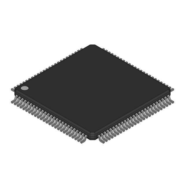
Packages
100-pin TQFP
T
Temperature
Commercial
Industrial
None
I
(0°C to 70°C)
(-40°C to 85°C)
Galvantech, Inc. 3080 Oakmead Village Drive, Santa Clara, CA 95051
Tel (408) 566-0688 Fax (408) 566-0699 Web Site www.galvantech.com
Rev. 11/9 9
Pentium is a trademark of Intel Corporation.
PowerPC is a trademark of IBM Corporation.
Galvantech, Inc. reserves the right to change
products or specifications without notice.
�GVT71128D32
128K X 32 SYNCHRONOUS BURST SRAM
GALVANTECH,
FUNCTIONAL BLOCK DIAGRAM
BYTE 1 WRITE
BW1#
BWE#
D
Q
CLK
BYTE 2 WRITE
BW2#
D
Q
GW#
BYTE 3 WRITE
BW3#
D
Q
BYTE 4 WRITE
ENABLE
D
CE2
Q
D
Q
byte 2 write
byte 1 write
CE#
Q
byte 3 write
D
byte 4 write
BW4#
CE2#
OE#
Power Down Logic
A16-A2
Address
Register
ADSC#
CLR
ADV#
A1-A0
Binary
Counter
& Logic
OUTPUT
REGISTER
D
Q
Output Buffers
Input
Register
ADSP#
128K x 8 x 4
SRAM Array
ZZ
DQ1-DQ32
MODE
NOTE:
November 20, 1999
Rev. 11/9 9
The Functional Block Diagram illustrates simplified device operation. See Truth Table, pin descriptions and timing
diagrams for detailed information.
2
Galvantech, Inc. reserves the right to change products or specifications without notice.
�GVT71128D32
128K X 32 SYNCHRONOUS BURST SRAM
GALVANTECH,
A6
A7
CE#
CE2
BW4#
BW3#
BW2#
BW1#
CE2#
VCC
VSS
CLK
GW#
BWE#
OE#
ADSC#
ADSP#
ADV#
A8
A9
PIN ASSIGNMENT (Top View)
100 99
NC
DQ17
DQ18
VCCQ
VSSQ
DQ19
DQ20
DQ21
DQ22
VSSQ
VCCQ
DQ23
DQ24
NC
VCC
NC
VSS
DQ25
DQ26
VCCQ
VSSQ
DQ27
DQ28
DQ29
DQ30
VSSQ
VCCQ
DQ31
DQ32
NC
98
97
96
95
94
93
92
91
90
89
88
87
86
85
84
83
82
81
1
80
2
79
3
78
4
77
5
76
6
75
7
74
8
73
9
72
10
71
11
70
12
69
13
68
14
67
100-pin PQFP
or
100-pin TQFP
15
16
17
66
65
64
18
63
19
62
20
61
21
60
22
59
23
58
24
57
25
56
26
55
27
54
28
53
29
52
30
51
32
33
34
35
36
37
38
39
40
41
42
43
44
45
46
47
48
49
50
MODE
A5
A4
A3
A2
A1
A0
NC
NC
VSS
VCC
NC
NC
A10
A11
A12
A13
A14
A15
A16
31
NC
DQ16
DQ15
VCCQ
VSSQ
DQ14
DQ13
DQ12
DQ11
VSSQ
VCCQ
DQ10
DQ9
VSS
NC
VCC
ZZ
DQ8
DQ7
VCCQ
VSSQ
DQ6
DQ5
DQ4
DQ3
VSSQ
VCCQ
DQ2
DQ1
NC
PIN DESCRIPTIONS
QFP PINS
37,
32,
44,
49,
36, 35, 34, 33,
100, 99, 82, 81,
45, 46, 47, 48,
50
93,94,95,96
87
SYMBOL
TYPE
DESCRIPTION
A0-A16
Input-
Addresses: These inputs are registered and must meet the setup and hold times around
the rising edge of CLK. The burst counter generates internal addresses associated with A0
and A1, during burst cycle and wait cycle .
Synchronous
BW1#,
BW2#,
BW3#,
BW4#
BWE#
InputSynchronous
InputSynchronous
88
GW#
InputSynchronous
89
CLK
InputSynchronous
98
CE#
Input-
Byte Write: A byte write is LOW for a WRITE cycle and HIGH for a READ cycle. BW1#
controls DQ1-DQ8. BW2# controls DQ9-DQ16. BW3# controls DQ17-DQ24. BW4#
controls DQ25-DQ32. Data I/O are high impedance if either of these inputs are LOW,
conditioned by BWE# being LOW.
Write Enable: This active LOW input gates byte write operations and must meet the setup
and hold times around the rising edge of CLK.
Global Write: This active LOW input allows a full 32-bit WRITE to occur independent of the
BWE# and BWn# lines and must meet the setup and hold times around the rising edge of
CLK.
Clock: This signal registers the addresses, data, chip enables, write control and burst
control inputs on its rising edge. All synchronous inputs must meet setup and hold times
around the clock’s rising edge.
Chip Enable: This active LOW input is used to enable the device and to gate ADSP#.
Synchronous
92
CE2#
Input-
Chip Enable: This active LOW input is used to enable the device.
Synchronous
November 20, 1999
Rev. 11/9 9
3
Galvantech, Inc. reserves the right to change products or specifications without notice.
�GVT71128D32
128K X 32 SYNCHRONOUS BURST SRAM
GALVANTECH,
PIN DESCRIPTIONS (continued)
QFP PINS
SYMBOL
TYPE
97
CE2
input-
DESCRIPTION
86
OE#
Input
Output Enable: This active LOW asynchronous input enables the data output drivers.
83
ADV #
Input-
Address Advance: This active LOW input is used to control the internal burst counter.
A HIGH on this pin generates wait cycle (no address advance).
Chip enable: This active HIGH input is used to enable the device.
Synchronous
Synchronous
84
ADSP#
InputSynchronous
85
ADSC#
InputSynchronous
Address Status Processor: This active LOW input, along with CE# being LOW,
causes a new external address to be registered and a READ cycle is initiated using
the new address .
Address Status Controller: This active LOW input causes device to be de-selected or
selected along with new external address to be registered. A READ or WRITE cycle is
initiated depending upon write control inputs.
31
MODE
InputStatic
Mode: This input selects the burst sequence. A LOW on this pin selects LINEAR
BURST. A NC or HIGH on this pin selects INTERLEAVED BURST .
64
ZZ
InputAsynchro-nous
Snooze: This active HIGH input puts the device in low power consumption standby
mode. For normal operation, this input has to be either LOW or NC (No Connect).
52, 53, 56, 57, 58, 59,
62, 63, 68, 69, 72-75,
78, 79, 2, 3, 6-9, 12, 13,
18, 19, 22-25, 28, 29
DQ1-DQ32
Input/
Outpu t
Data Inputs/Outputs: First Byte is DQ1-DQ8. Second Byte is DQ9-DQ16. Third Byte
is DQ17-DQ24. Fourth Byte is DQ25-DQ32. Input data must meet setup and hold
times around the rising edge of CLK.
15, 41, 65, 9 1
VCC
Supply
Power Supply: +3.3V -5% to +10%. Pin 14 does not have to be connected directly to
VCCas long as it is greater than VIH .
Ground: GN D
17, 40, 67, 9 0
VSS
Ground
4, 11, 20, 27, 54, 61, 70,
77
VCCQ
I/O Supply
Output Buffer Supply: +3.3V -5% to +10%. For 2.5V I/O: 2.375V to VCC.
5, 10, 21, 26, 55, 60, 71,
76
VSSQ
I/O Ground
Output Buffer Ground: GND
1, 14, 16, 30, 38, 39, 42,
43, 50, 51, 66, 80
NC
-
No Connect: These signals are not internally connected.
BURST ADDRESS TABLE (MODE = NC/VCC )
First Address
(external)
Second Address
(internal)
Third Address
(internal)
Fourth Address
(internal)
A...A00
A...A01
A...A10
A...A11
A...A01
A...A00
A...A11
A...A10
A...A10
A...A11
A...A00
A...A01
A...A11
A...A10
A...A01
A...A00
BURST ADDRESS TABLE (MODE = GND)
First Address
(external)
Second Address
(internal)
Third Address
(internal)
Fourth Address
(internal)
A...A00
A...A01
A...A10
A...A11
A...A01
A...A10
A...A11
A...A00
A...A10
A...A11
A...A00
A...A01
A...A11
A...A00
A...A01
A...A10
PARTIAL TRUTH TABLE FOR READ/WRIT E
FUNCTION
GW#
BWE#
BW1#
BW2#
BW3#
BW4#
READ
H
H
X
X
X
X
READ
H
L
H
H
H
H
WRITE one byte
H
L
L
H
H
H
WRITE all bytes
H
L
L
L
L
L
WRITE all bytes
L
X
X
X
X
X
November 20, 1999
Rev. 11/9 9
4
Galvantech, Inc. reserves the right to change products or specifications without notice.
�GVT71128D32
128K X 32 SYNCHRONOUS BURST SRAM
GALVANTECH,
TRUTH TABLE
ADDRESS
USED
CE#
CE2#
CE2
Deselected Cycle, Power Down
None
H
X
X
X
Deselected Cycle, Power Down
None
L
X
L
L
Deselected Cycle, Power Down
None
L
H
X
Deselected Cycle, Power Down
None
L
X
Deselected Cycle, Power Down
None
L
READ Cycle, Begin Burs t
External
READ Cycle, Begin Burs t
OPERATION
ADV#
WRITE#
OE#
CLK
DQ
L
X
X
X
L-H
High-Z
X
X
X
X
L-H
High-Z
L
X
X
X
X
L-H
High-Z
L
H
L
X
X
X
L-H
High-Z
H
X
H
L
X
X
X
L-H
High-Z
L
L
H
L
X
X
X
L
L-H
Q
External
L
L
H
L
X
X
X
H
L-H
High-Z
WRITE Cycle, Begin Burst
External
L
L
H
H
L
X
L
X
L-H
D
READ Cycle, Begin Burs t
External
L
L
H
H
L
X
H
L
L-H
Q
READ Cycle, Begin Burs t
External
L
L
H
H
L
X
H
H
L-H
High-Z
READ Cycle, Continue Burst
Next
X
X
X
H
H
L
H
L
L-H
Q
READ Cycle, Continue Burst
Next
X
X
X
H
H
L
H
H
L-H
High-Z
READ Cycle, Continue Burst
Next
H
X
X
X
H
L
H
L
L-H
Q
READ Cycle, Continue Burst
Next
H
X
X
X
H
L
H
H
L-H
High-Z
WRITE Cycle, Continue Burst
Next
X
X
X
H
H
L
L
X
L-H
D
WRITE Cycle, Continue Burst
Next
H
X
X
X
H
L
L
X
L-H
D
READ Cycle, Suspend Burs t
Current
X
X
X
H
H
H
H
L
L-H
Q
READ Cycle, Suspend Burs t
Current
X
X
X
H
H
H
H
H
L-H
High-Z
READ Cycle, Suspend Burs t
Current
H
X
X
X
H
H
H
L
L-H
Q
READ Cycle, Suspend Burs t
Current
H
X
X
X
H
H
H
H
L-H
High-Z
WRITE Cycle, Suspend Burst
Current
X
X
X
H
H
H
L
X
L-H
D
WRITE Cycle, Suspend Burst
Current
H
X
X
X
H
H
L
X
L-H
D
Note:
1.
2.
3.
4.
5.
6.
7.
November 20, 1999
Rev. 11/9 9
ADSP # ADSC#
X means “don’t care.” H means logic HIGH. L means logic LOW. WRITE# = L means [BWE# +
BW1#*BW2#*BW3#*BW4#]*GW# equals LOW. WRITE# = H means [BWE# + BW1#*BW2#*BW3#*BW4#]*GW# equals
HIGH.
BW1# enables write to DQ1-DQ8. BW2# enables write to DQ9-DQ16. BW3# enables write to DQ17-DQ24. BW4# enables
write to DQ25-DQ32.
All inputs except OE# must meet setup and hold times around the rising edge (LOW to HIGH) of CLK.
Suspending burst generates wait cycle.
For a write operation following a read operation, OE# must be HIGH before the input data required setup time plus High-Z time
for OE# and staying HIGH throughout the input data hold time.
This device contains circuitry that will ensure the outputs will be in High-Z during power-up.
ADSP# LOW along with chip being selected always initiates an READ cycle at the L-H edge of CLK. A WRITE cycle can be
performed by setting WRITE# LOW for the CLK L-H edge of the subsequent wait cycle. Refer to WRITE timing diagram for
clarification.
5
Galvantech, Inc. reserves the right to change products or specifications without notice.
�GALVANTECH,
GVT71128D32
128K X 32 SYNCHRONOUS BURST SRAM
*Stresses greater than those listed uunder “Absolute Maximum
Ratings” may cause permanent damage to the device.This is a stress
rating only and functional operation of the device at these or any
other conditions above those indicated in the operational sections of
this specification is not implied. Exposure to absolute maximum
rating conditions for extended periods may affect reliability.
ABSOLUTE MAXIMUM RATINGS*
Voltage on VCC Supply Relative to VSS........-0.5V to +4.6V
VIN ...........................................................-0.5V to VCC+0.5V
Storage Temperature (plastic) .........................-55o C to +150 o
Junction Temperature .....................................................+150 o
Power Dissipation ...........................................................1.0W
Short Circuit Output Current .........................................50mA
DC ELECTRICAL CHARACTERISTICS AND RECOMMENDED OPERATING CONDITIONS
(All
Temperature Ranges; VCC = 3.3V -5 to +10% unless otherwise noted)
DESCRIPTION
CONDITIONS
Input High (Logic 1) Voltage
SYMBOL
MIN
MAX
UNITS
NOTES
Data Inputs (DQxx)
V I HD
2.0
VCCQ+0.3
V
1,2
All Other Inputs
V IH
2.0
4.6
V
1,2
V Il
-0.3
0.8
V
1, 2
14
Input Low (Logic 0) Voltage
Input Leakage Current
0V < V IN < VCC
IL I
-2
2
uA
Output Leakage Current
Output(s) disabled,
0V < V OUT < VCC
IL O
-2
2
uA
Output High Voltage
IOH = -4.0mA
V OH
2.4
Output Low Voltage
IOL = 8.0mA
V OL
Supply Voltage
V
1, 11
0.4
V
1, 11
VCC
3.1
3.6
V
1
I/O Supply Voltage (3.3V I/O)
VCCQ
3.1
3.6
V
1
I/O Supply Voltage (2.5V I/O)
VCCQ
2.375
VCC
V
1
DESCRIPTION
CONDITIONS
SYM
TYP
-4
-5
-6
-7
Power Supply
Current: Operating
UNITS NOTES
Device selected; all inputs < V IL or >
V IH ;cycle time > tKC MIN; VCC =MAX;
outputs open
Icc
80
225
225
185
120
mA
3, 12,
13
CMOS Standby
Device deselected; VCC = MAX;
all inputs < VSS +0.2 or >VCC -0.2;
all inputs static; CLK frequency = 0
ISB2
0.2
2
2
2
2
mA
12,13
TTL Standby
Device deselected; all inputs < V IL
or > V IH; all inputs static;
VCC = MAX; CLK frequency = 0
ISB3
8
18
18
18
18
mA
12,13
Clock Runnin g
Device deselected;
all inputs < V IL or > V IH ; VCC = MAX;
CLK cycle time > t KC MIN
ISB4
12
30
30
25
20
mA
12,13
CAPACITANCE
DESCRIPTION
CONDITIONS
Input Capacitance
TA = 25 o C; f = 1 MHz
VCC = 3.3V
Input/Output Capacitance (DQ)
SYMBOL
TYP
MAX
UNITS
NOTES
CI
3
4
pF
4
CO
6
7
pF
4
THERMAL CONSIDERATIO N
DESCRIPTION
CONDITIONS
Thermal Resistance - Junction to Ambient
Still air, soldered on 4.25 x
1.125 inch 4-layer PCB
Thermal Resistance - Junction to Case
November 20, 1999
Rev. 11/9 9
SYMBOL TQFP TYP
6
UNITS
ΘJ A
20
o C/W
Θ JC
1
o C/W
NOTES
Galvantech, Inc. reserves the right to change products or specifications without notice.
�GVT71128D32
128K X 32 SYNCHRONOUS BURST SRAM
GALVANTECH,
AC ELECTRICAL CHARACTERISTICS
(Note 5) (All Temperature Ranges; VCC = 3.3V -5 to +10% )
-4
DESCRIPTION
-5
MAX
MIN
-6
MAX
MIN
-7
SY M
MIN
MAX
MIN
MAX
UNIT S NOTES
Clock cycle tim e
tKC
10
10
12
15
ns
Clock HIGH time
tKH
4
4
4
5
ns
Clock LOW tim e
tKL
4
4
4
5
ns
Cloc k
Output Times
t KQ
Clock to output valid
4.8
5
6
7
ns
tKQ X
2
2
2
2
Clock to output in Low-Z
t KQLZ
3
3
3
3
ns
6,7
Clock to output in High-Z
t KQH Z
5
5
5
6
ns
6,7
OE to output valid
t OEQ
5
5
6
7
ns
9
OE to output in Low-Z
t OELZ
ns
6,7
OE to output in High-Z
t OEHZ
ns
6,7
Clock to output invalid
0
0
0
4
4
ns
0
5
6
Setup Times
Address, Controls and Data In
tS
2.0
2.5
2.5
2.5
ns
10
tH
0.5
0.5
0.5
0.5
ns
10
Hold Times
Address, Controls and Data In
CAPACITANCE DERATING
DESCRIPTION
Clock to output valid
November 20, 1999
Rev. 11/9 9
SYMBOL
TYP
∆ tKQ
0.016
MAX
7
UNITS
NOTES
ns / pF
15
Galvantech, Inc. reserves the right to change products or specifications without notice.
�GVT71128D32
128K X 32 SYNCHRONOUS BURST SRAM
GALVANTECH,
OUTPUT LOADS FOR 3.3V I/O
AC TEST CONDITIONS FOR 3.3V I/O
Input pulse levels
DQ
0V to 3.0V
Z0 = 50 Ω
50Ω
30 pF
Input rise and fall times
1.5ns
Input timing reference levels
1.5V
Output reference levels
1.5V
Fig. 1 OUTPUT LOAD EQUIVALENT
See Figures 1 and 2
3.3v
Output load
Vt = 1.5V
317Ω
AC TEST CONDITIONS FOR 2.5V I/O
Input pulse levels
DQ
351Ω
0V to 2.5V
Input slew rate
5 pF
1.0V/ns
Output rise and fall times(max)
1.8ns
Input timing reference levels
1.25V
Output reference levels
1.25V
Output load
Fig. 2 OUTPUT LOAD EQUIVALENT
OUTPUT LOADS FOR 2.5V I/O
DQ
See Figures 3
Z0 = 50Ω
50Ω
Vt = 1.25V
Fig. 3 OUTPUT LOAD EQUIVALENT
10. This is a synchronous device. All synchronous inputs must meet
specified setup and hold time, except for “don’t care” as defined
in the truth table.
NOTES
1.
All voltages referenced to VSS (GND).
2.
Overshoot:
Undershoot:
3.
Ic c is given with no output current. Ic c increases with greater
output loading and faster cycle times.
12. “Device Deselected” means the device is in POWER -DOWN
mode as defined in the truth table. “Device Selected” means the
device is active.
4.
This parameter is sampled.
13. Typical values are measured at 3.3V, 25oC and 20ns cycle time.
5.
Test conditions as specified with the output loading as shown in
Fig. 1 unless otherwise noted.
6.
Output loading is specified with CL=5pF as in Fig. 2.
7.
At any given temperature and voltage condition, t KQHZ is less
than t KQLZ and t OEHZ is less than t OELZ.
8.
A READ cycle is defined by byte write enables all HIGH or
ADSP# LOW along with chip enables being active for the
required setup and hold times. A WRITE cycle is defined by at
one byte or all byte WRITE per READ/WRITE TRUTH
TABLE.
9.
OE# is a “don’t care” when a byte write enable is sampled LOW.
November 20, 1999
Rev. 11/9 9
VIH ≤ +6.0V for t ≤ t KC /2.
VIL ≤ -2.0V for t ≤ t KC /2
11. AC I/O curves are available upon request.
14. MODE pin has an internal pull-up and ZZ pin has an internal
pull-down. These two pins exhibit an input leakage current of
+30 µA.
15. Capacitance derating applies to capacitance different from the
load capacitance shown in Fig. 1 or Fig. 3, for 3.3V or 2.5V I/O
respectively
8
Galvantech, Inc. reserves the right to change products or specifications without notice.
�GVT71128D32
128K X 32 SYNCHRONOUS BURST SRAM
GALVANTECH,
READ TIMING
t
KC
t
KL
CLK
t
t
S
KH
ADSP#
tH
ADSC#
tS
ADDRESS
BW1#, BW2#,
BW3#, BW4#,
BWE#, GW#
A1
A2
tH
CE#
(See Note)
t
S
ADV#
t
H
OE#
t
tKQLZ
DQ
tKQ
tOEQ
KQ
tOELZ
Q(A1)
Q(A2)
SINGLE READ
Q(A2+1)
Q(A2+2)
Q(A2+3)
Q(A2)
Q(A2+1)
BURST READ
Note: CE# active in this timing diagram means that all chip enables CE#, CE2, and CE2# are active.
November 20, 1999
Rev. 11/9 9
9
Galvantech, Inc. reserves the right to change products or specifications without notice.
�GVT71128D32
128K X 32 SYNCHRONOUS BURST SRAM
GALVANTECH,
WRITE TIMING
CLK
t
S
ADSP#
t
H
ADSC#
t
ADDRESS
S
A1
A2
A3
tH
BW1#, BW2#,
BW3#, BW4#,
BWE#
GW#
CE#
(See Note)
t
S
ADV#
t
H
OE#
t
OEHZ
tKQX
DQ
Q
D(A1)
D(A2)
D(A2+1)
SINGLE WRITE
D(A2+1)
D(A2+2)
D(A2+3)
D(A3)
BURST WRITE
D(A3+1)
D(A3+2)
BURST WRITE
Note: CE# active in this timing diagram means that all chip enables CE#, CE2, and CE2# are active.
November 20, 1999
Rev. 11/9 9
10
Galvantech, Inc. reserves the right to change products or specifications without notice.
�GVT71128D32
128K X 32 SYNCHRONOUS BURST SRAM
GALVANTECH,
READ/WRITE TIMING
CLK
t
S
ADSP#
t
H
ADSC#
t
ADDRESS
A1
S
A2
t
BW1#, BW2#,
BW3#, BW4#,
BWE#, GW#
A3
A4
A5
H
CE#
(See Note)
ADV#
OE#
DQ
Q(A1)
Single
Reads
Q(A2)
D(A3)
Q(A3)
Q(A4)
Q(A4+1)
Q(A4+2)
D(A5)
D(A5+1)
Pass Through
Single Write
Burst Read
Burst Write
Note: CE# active in this timing diagram means that all chip enables CE#, CE2, and CE2# are active.
November 20, 1999
Rev. 11/9 9
11
Galvantech, Inc. reserves the right to change products or specifications without notice.
�GALVANTECH,
GVT71128D32
128K X 32 SYNCHRONOUS BURST SRAM
100 Pin TQFP Package Dimensions
16.00 + 0.10
14.00 + 0.10
#1
22.00 + 0.10
20.00 + 0.10
1.40 + 0.05
1.60 Max
0.65 Basic
0.30 + 0.08
0.60 + 0.15
Note: All dimensions in Millimeters
November 20, 1999
Rev. 11/9 9
12
Galvantech, Inc. reserves the right to change products or specifications without notice.
�GALVANTECH,
GVT71128D32
128K X 32 SYNCHRONOUS BURST SRAM
Ordering Information
GVT 71128D32 X - X X
Galvantech Prefix
Temperature (Blank = Commercial
I = Industrial)
Part Number
Speed (4 = 4.8ns access/10ns cycle
5 = 5ns access/10ns cycle
6 = 6ns access/12ns cycle
7 = 7ns access/15ns cycle)
Package (T = 100 PIN TQFP)
November 20, 1999
Rev. 11/9 9
13
Galvantech, Inc. reserves the right to change products or specifications without notice.
�


 工商网监
湘ICP备2023018690号
工商网监
湘ICP备2023018690号
