350A
CY7C1350A/GVT71128ZC36
128Kx36 Pipelined SRAM with NoBL™ Architecture
Features
• Zero Bus Latency, no dead cycles between write and
read cycles
• Fast clock speed: 143, 133 and 100 MHzInternally synchronized registered outputs eliminate the need to control OE
• Single 3.3V –5% and +5% power supply VCC
• Separate VCCQ for 3.3V or 2.5V I/O
• Single R/W (Read/Write) control pin
• Positive clock-edge triggered, address, data, and control signal registers for fully pipelined applications
• Interleaved or linear 4-word burst capability
• Individual byte write (BWa–BWd) control (may be tied
LOW)
• CKE pin to enable clock and suspend operations
• Three chip enables for simple depth expansion
• Snooze Mode for low-power standby
• Automatic power-down
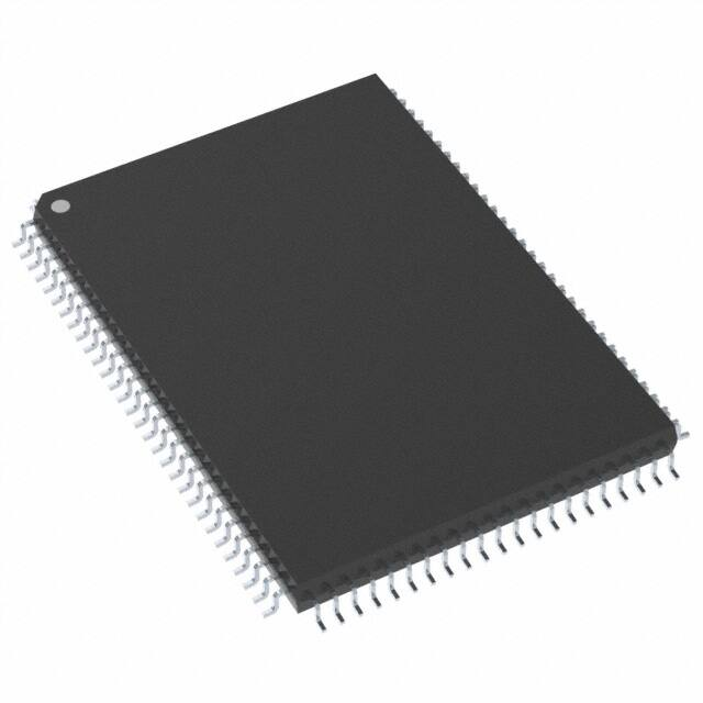
• Packaged in a JEDEC standard 100-pin TQFP package
Functional Description
The CY7C1350A/GVT71128ZC36 SRAM are designed to
eliminate dead cycles when transitioning from Read to Write
or vice versa. This SRAM is optimized for 100 percent bus
utilization and achieve Zero Bus Latency (ZBL)/No Bus Latency™ (NoBL™). It integrates 131,072x36 SRAM cells with advanced synchronous peripheral circuitry and a 2-bit counter for
internal burst operation. The Cypress Synchronous Burst
SRAM family employs high-speed, low-power CMOS designs
using advanced triple-layer polysilicon, double-layer metal
technology. Each memory cell consists of four transistors and
two high-valued resistors.
All synchronous inputs are gated by registers controlled by a
positive-edge-triggered Clock Input (CLK). The synchronous
inputs include all addresses, all data inputs, depth-expansion
Chip Enables (CE, CE2 and CE2), Cycle Start Input (ADV/LD),
Clock Enable (CKE), Byte Write Enables (BWa, BWb, BWc,
and BWd), and Read-Write Control (R/W).
Address and control signals are applied to the SRAM during
one clock cycle, and two cycles later, its associated data occurs, either read or write.
A clock enable (CKE) pin allows operation of the
CY7C1350A/GVT71128ZC36 to be suspended as long as
necessary. All synchronous inputs are ignored when (CKE) is
HIGH and the internal device registers will hold their previous
values.
There are three chip enable pins (CE, CE2, CE2) that allow the
user to deselect the device when desired. If any one of these
three are not active when ADV/LD is LOW, no new memory
operation can be initiated and any burst cycle in progress is
stopped. However, any pending data transfers (read or write)
will be completed. The data bus will be in high-impedance
state two cycles after chip is deselected or a write cycle is
initiated.
The CY7C1350A/GVT71128ZC36 has an on-chip 2-bit burst
counter. In the burst mode, the CY7C1350A/GVT71128ZC36
provides four cycles of data for a single address presented to
the SRAM. The order of the burst sequence is defined by the
MODE input pin. The MODE pin selects between linear and
interleaved burst sequence. The ADV/LD signal is used to load
a new external address (ADV/LD = LOW) or increment the
internal burst counter (ADV/LD = HIGH)
Output Enable (OE), Snooze Enable (ZZ) and burst sequence
select (MODE) are the asynchronous signals. OE can be used
to disable the outputs at any given time. ZZ may be tied to
LOW if it is not used.
The CY7C1350A/GVT71128ZC36 utilizes a high-performance high-volume 3.3V CMOS process, and is packaged in
a JEDEC Standard 14-mm x 20-mm 100-pin plastic quad flatpack (TQFP) for high board density.
Selection Guide
7C1350A-143
71128ZC36-4
7C1350A-133
71128ZC36-5
7C1350A-133
71128ZC36-6
7C1350A-100
71128ZC36-7
4.0
4.2
4.2
5.0
Com’l
400
380
380
300
Maximum CMOS Standby Current (mA) Com’l
10
10
10
10
Maximum Access Time (ns)
Maximum Operating Current (mA)
No Bus Latency and NoBL are trademarks of Cypress Semiconductor Corporation.
Cypress Semiconductor Corporation
Document #: 38-05124 Rev. **
•
3901 North First Street
•
San Jose
•
CA 95134
•
408-943-2600
Revised September 12, 2001
�CY7C1350A/GVT71128ZC36
.
Functional Block Diagram—128Kx36[1]
ZZ
MODE
Address
128K x 9 x 4
SRAM Array
CKE#
ADV/LD#
Control
R/W#
DI
CE#, CE2#, CE2
Input
Registers
DO
BWa#, BWb#
BWc#, BWd#
SA0, SA1, SA
Control Logic
Mux
Sel
Functional Block Diagram—512Kx18[1]
CLK
OE#
Output Registers
Output Buffers
DQa-DQd,
DQPa, DQPb
DQPc, DQPd
Note:
1. The Functional Block Diagram illustrates simplified device operation. See Truth Table, pin descriptions and timing diagrams for detailed information.
Document #: 38-05124 Rev. **
Page 2 of 16
�CY7C1350A/GVT71128ZC36
Pin Configurations
SA
SA
100
99
98
97
96
95
94
93
92
91
90
89
88
87
86
85
84
83
82
81
SA
SA
CE
CE2
BWd
BWc
BWb
BWa
CE2
VCC
VSS
CLK
R/W
CKE
OE
ADV/LD
NC
SA
100-Pin TQFP Package
DQPc
DQc
DQc
VCCQ
VSS
DQc
DQc
DQc
DQc
VSS
VCCQ
CY7C1350A/
GVT71128ZC36
(128K x 36)
80
79
78
77
76
75
74
73
72
71
70
69
68
67
66
65
64
63
62
61
60
59
58
57
56
55
54
53
52
51
DQPb
DQb
DQb
VCCQ
VSS
DQb
DQb
DQb
DQb
VSS
VDDQ
DQb
DQb
VSS
VCC
VCC
ZZ
DQa
DQa
VCCQ
VSS
DQa
DQa
DQa
DQa
VSS
VCCQ
DQa
DQa
DQPa
NC
NC
SA
SA
SA
SA
SA
SA
SA
MODE
SA
SA
SA
SA
SA1
SA0
NC
NC
VSS
VCC
31
32
33
34
35
36
37
38
39
40
41
42
43
44
45
46
47
48
49
50
DQc
DQc
VCC
VCC
VCC
VSS
DQd
DQd
VCCQ
VSS
DQd
DQd
DQd
DQd
VSS
VDDQ
DQd
DQd
DQPd
1
2
3
4
5
6
7
8
9
10
11
12
13
14
15
16
17
18
19
20
21
22
23
24
25
26
27
28
29
30
Pin Descriptions
TQFP Pins
Name
Type
Description
37,
36,
32, 33, 34, 35,
44, 45, 46, 47,
48, 49, 50, 81,
82, 83, 99, 100
SA0,
SA1,
SA
InputSynchronous
Synchronous Address Inputs: The address register is triggered by a combination
of the rising edge of CLK, ADV/LD LOW, CKE LOW and true chip enables. SA0
and SA1 are the two least significant bits of the address field and set the internal
burst counter if burst cycle is initiated.
93,
94,
95,
96
BWa,
BWb,
BWc,
BWd
InputSynchronous
Synchronous Byte Write Enables: Each 9-bit byte has its own active LOW byte
write enable. On load write cycles (when R/W and ADV/LD are sampled LOW),
the appropriate byte write signal (BWx) must be valid. The byte write signal must
also be valid on each cycle of a burst write. Byte write signals are ignored when
R/W is sampled HIGH. The appropriate byte(s) of data are written into the device
two cycles later. BWa controls DQa pins; BWb controls DQb pins; BWc controls
DQc pins; BWd controls DQd pins. BWx can all be tied LOW if always doing write
to the entire 36-bit word.
Document #: 38-05124 Rev. **
Page 3 of 16
�CY7C1350A/GVT71128ZC36
Pin Descriptions (continued)
TQFP Pins
Name
Type
Description
87
CKE
InputSynchronous
Synchronous Clock Enable Input: When CKE is sampled HIGH, all other synchronous inputs, including clock are ignored and outputs remain unchanged. The
effect of CKE sampled HIGH on the device outputs is as if the LOW-to-HIGH clock
transition did not occur. For normal operation, CKE must be sampled LOW at
rising edge of clock.
88
R/W
InputSynchronous
Read Write: R/W signal is a synchronous input that identifies whether the current
loaded cycle and the subsequent burst cycles initiated by ADV/LD is a Read or
Write operation. The data bus activity for the current cycle takes place two clock
cycles later.
89
CLK
InputSynchronous
Clock: This is the clock input to CY7C1350A/GVT71128ZC36. Except for OE, ZZ
and MODE, all timing references for the device are made with respect to the rising
edge of CLK.
98, 92
CE,
CE2
InputSynchronous
Synchronous Active LOW Chip Enable: CE and CE2 are used with CE2 to enable
the CY7C1350A/GVT71128ZC36. CE or CE2 sampled HIGH or CE2 sampled
LOW, along with ADV/LD LOW at the rising edge of clock, initiates a deselect
cycle. The data bus will be High-Z two clock cycles after chip deselect is initiated.
97
CE2
InputSynchronous
Synchronous Active HIGH Chip Enable: CE2 is used with CE and CE2 to enable
the chip. CE2 has inverted polarity but otherwise is identical to CE and CE2.
86
OE
Input
Asynchronous Output Enable: OE must be LOW to read data. When OE is HIGH,
the I/O pins are in high-impedance state. OE does not need to be actively controlled for read and write cycles. In normal operation, OE can be tied LOW.
85
ADV/L
D
InputSynchronous
Advance/Load: ADV/LD is a synchronous input that is used to load the internal
registers with new address and control signals when it is sampled LOW at the
rising edge of clock with the chip is selected. When ADV/LD is sampled HIGH,
then the internal burst counter is advanced for any burst that was in progress. The
external addresses and R/W are ignored when ADV/LD is sampled HIGH.
31
MODE
InputStatic
Burst Mode: When MODE is HIGH or NC, the interleaved burst sequence is
selected. When MODE is LOW, the linear burst sequence is selected. MODE is
a static DC input.
64
ZZ
52, 53, 56-59,
62, 63, 68, 69,
72-75, 78, 79
2, 3, 6–9, 12, 13
18, 19, 22–25,
28, 29
DQa
DQb
DQc
DQd
Input/
Output
Data Inputs/Outputs: Both the data input path and data output path are registered
and triggered by the rising edge of CLK. Byte “a” is DQa pins; Byte “b” is DQb
pins; Byte “c” is DQc pins; Byte “d” is DQd pins.
51, 80, 1, 30
DQPa,
DQPb,
DQPc,
DQPd
Input/
Output
Parity Inputs/Outputs: Both the data input path and data output path are registered
and triggered by the rising edge of CLK. DQPa is parity bit for Byte “a”; DQPb is
parity bit for Byte “b”; DQPc is parity bit for Byte “c”; DQPd is parity bit for Byte “d”.
14, 15, 16, 41,
65, 66, 91
VCC
Supply
Power Supply: +3.3V –5% and +5%.
5, 10, 17, 21, 26,
40, 55, 60, 67,
71, 76, 90
VSS
Ground
Ground: GND.
4, 11, 20, 27, 54,
61, 70, 77
VCCQ
I/O Supply
Output Buffer Supply: +3.3V –0.165V and +0.165V for 3.3V I/O. +2.5V –0.125V
and +0.4V for 2.5V I/O.
38, 39, 42, 43,
83, 84
NC
-
No Connect: These signals are not internally connected. It can be left floating or
be connected to VCC or to GND.
InputSnooze Enable: This active HIGH input puts the device in low power consumption
Asynchronous standby mode. For normal operation, this input has to be either LOW or NC.
Document #: 38-05124 Rev. **
Page 4 of 16
�CY7C1350A/GVT71128ZC36
Interleaved Burst Address Table
(MODE = VCC or NC)
Linear Burst Address Table
(MODE = VSS)
First
Address
(external)
Second
Address
(internal)
Third
Address
(internal)
Fourth
Address
(internal)[2]
First
Address
(external)
Second
Address
(internal)
Third
Address
(internal)
Fourth
Address
(internal)[2]
A...A00
A...A01
A...A10
A...A11
A...A00
A...A01
A...A10
A...A11
A...A01
A...A00
A...A11
A...A10
A...A01
A...A10
A...A11
A...A00
A...A10
A...A11
A...A00
A...A01
A...A10
A...A11
A...A00
A...A01
A...A11
A...A10
A...A01
A...A00
A...A11
A...A00
A...A01
A...A10
Partial Truth Table for Read/Write[3]
Function
R/W
BWa
BWb
BWc
BWd
H
X
X
X
X
No Write
L
H
H
H
H
Write Byte a (DQa, DQPa)[4]
L
L
H
H
H
[4]
L
H
L
H
H
[4]
L
H
H
L
H
[4]
L
H
H
H
L
L
L
L
L
L
Read
Write Byte b (DQb, DQPb)
Write Byte c (DQc, DQPc)
Write Byte d (DQd, DQPd)
Write all bytes
Functional Timing Diagram[5, 6]
CYCLE
n+19
n+20
n+21
n+22
n+23
n+24
n+25
n+26
n+27
ADDRESS
(SA0, SA1, SA)
A19
A20
A21
A22
A23
A24
A25
A26
A27
CONTROL
(R/W#, BWx#,
ADV/LD#)
C19
C20
C21
C22
C23
C24
C25
C26
C27
DQ17
DQ18
DQ19
DQ20
DQ21
DQ22
DQ23
DQ24
DQ25
CLOCK
DATA
DQ[a:d]
DQP[a:d]
Notes:
2. Upon completion of the Burst sequence, the counter wraps around to its initial state and continues counting.
3. L means logic LOW. H means logic HIGH. X means “Don’t Care.”
4. Multiple bytes may be selected during the same cycle.
5. This assumes that CKE, CE, CE2 and CE2 are all True.
6. All addresses, control and data-in are only required to meet set-up and hold time with respect to the rising edge of clock. Data out is valid after a clock-to-data
delay from the rising edge of clock.
Document #: 38-05124 Rev. **
Page 5 of 16
�CY7C1350A/GVT71128ZC36
Truth Table[7, 8, 9, 10, 11, 12, 13, 14, 15]
OPERATION
Deselect Cycle
[16]
Continue Deselect/NOP
Read Cycle (Begin Burst)
Read Cycle (Continue Burst)
[16]
Dummy Read (Begin Burst)[17]
Dummy Read (Continue Burst)[16, 17]
Write Cycle (Begin Burst)
Write Cycle (Continue Burst)
[16]
Abort Write (Begin Burst)[17]
Abort Write (Continue Burst)[16, 17]
[18]
Ignore Clock Edge/NOP
Previous
Cycle
Address
Used
R/W
ADV/LD
CE
CKE
BWx
OE
DQ
(2 cycles later)
X
X
X
L
H
L
X
X
High-Z
Deselect
X
X
H
X
L
X
X
High-Z
X
External
H
L
L
L
X
X
Q
Read
Next
X
H
X
L
X
X
Q
X
External
H
L
L
L
X
H
High-Z
Read
Next
X
H
X
L
X
H
High-Z
X
External
L
L
L
L
L
X
D
Write
Next
X
H
X
L
L
X
D
X
External
L
L
L
L
H
X
High-Z
Write
Next
X
H
X
L
H
X
High-Z
X
X
X
H
X
H
X
X
-
Notes:
7. L means logic LOW. H means logic HIGH. X means “Don’t Care.” High-Z means High Impedance. BWx = L means [BWa*BWb*BWc*BWd] equals LOW. BWx
= H means [BWa*BWb*BWc*BWd] equals HIGH.
8. CE equals H means CE and CE2 are LOW along with CE2 being HIGH. CE equals L means CE or CE2 is HIGH or CE2 is LOW. CE equals X means CE, CE2,
and CE2 are “Don’t Care.”
9. BWa enables WRITE to byte “a” (DQa pins). BWb enables WRITE to byte “b” (DQb pins). BWc enables WRITE to byte “c” (DQc pins). BWd enables WRITE to
byte “d” (DQd pins).
10. The device is not in Snooze Mode, i.e. the ZZ pin is LOW.
11. During Snooze Mode, the ZZ pin is HIGH and all the address pins and control pins are “Don’t Care.” The SNOOZE MODE can only be entered two cycles after
the Write cycle, otherwise the Write cycle may not be completed.
12. All inputs, except OE, ZZ, and MODE pins, must meet set-up time and hold time specification against the clock (CLK) LOW-to-HIGH transition edge.
13. OE may be tied to LOW for all the operation. This device automatically turns off the output driver during WRITE cycle.
14. Device outputs are ensured to be in High-Z during device power-up.
15. This device contains a 2-bit burst counter. The address counter is incremented for all Continue Burst cycles. Address wraps to the initial address every fourth
burst cycle.
16. Continue Burst cycles, whether Read or Write, use the same control signals. The type of cycle performed, Read or Write, depends upon the R/W control signal
at the Begin Burst cycle. A Continue Deselect cycle can only be entered if a Deselect cycle is executed first.
17. Dummy Read and Abort Write cycles can be entered to set up subsequent Read or Write cycles or to increment the burst counter.
18. When an Ignore Clock Edge cycle enters, the output data (Q) will remain the same if the previous cycle is Read cycle or remain High-Z if the previous cycle is
Write or Deselect cycle.
Document #: 38-05124 Rev. **
Page 6 of 16
�CY7C1350A/GVT71128ZC36
Maximum Ratings
Power Dissipation ......................................................... 2.0W
(Above which the useful life may be impaired. For user guidelines, not tested.)
Short Circuit Output Current ....................................... 50 mA
Operating Range
Voltage on VCC Supply Relative to VSS ......... –0.5V to +4.6V
VIN ...........................................................–0.5V to VCC+0.5V
Storage Temperature (plastic) .................... –55°C to +125°C
Junction Temperature ............................................... +125°C
Range
Ambient
Temperature[19]
VCC/VCCQ
0°C to +70°C
3.3V ± 5%
Com’l
Electrical Characteristics Over the Operating Range [20]
Parameter
VIHD
Description
Test Conditions
Input High (Logic 1) Voltage
[21, 22]
VIH
Min.
Max.
Unit
Data Inputs (DQxx)
2.0
VCC+0.3
V
All Other Inputs
2.0
4.6
V
[21, 22]
VIl
Input Low (Logic 0) Voltage
–0.5
0.8
V
ILI
Input Leakage Current
0V < VIN < VCC
-
5
µA
ILI
MODE and ZZ Input Leakage Current[21] 0V < VIN < VCC
-
30
µA
ILO
Output Leakage Current
-
5
µA
VOH
VOL
VCC
VCCQ
Parameter
Output High Voltage
Output Low Voltage
[21]
[21]
Output(s) disabled, 0V < VOUT < VCC
IOH = –5.0 mA for 3.3V I/O
2.4
V
IOH = –1.0 mA for 2.5V I/O
2.0
V
IOL = 8.0 mA
0.4
V
3.135
3.465
V
3.3V I/O
3.135
3.465
V
2.5V I/O
2.4
2.9
V
[21]
Supply Voltage
I/O Supply Voltage
[21]
Description
Conditions
Typ.
Device selected; all inputs < VILor > 150
VIH; cycle time > tKC min.; VCC =Max.;
outputs open, ADV/LD = X, f = fMAX2
143
MHz/
-4
133
MHz/
-5
117
MHz/
-6
100
MHz/
-7
Unit
400
380
350
300
mA
ICC
Power Supply Current:
Operating[24, 25, 26, 27]
ISB2
CMOS Standby[25, 26, 27] Device deselected; VCC = Max.;
all inputs < VSS + 0.2 or > VCC – 0.2;
all inputs static; CLK frequency = 0
5
10
10
10
10
mA
ISB3
TTL Standby[25, 26, 27]
20
40
40
40
40
mA
ISB4
Clock Running[25, 26, 27] Device deselected;
all inputs < VIL or > VIH; VCC = MAX;
CLK cycle time > tKC Min.
50
95
85
80
70
mA
Device deselected; all inputs < VIL
or > VIH; all inputs static;
VCC = Max.; CLK frequency = 0
Notes:
19. TA is the case temperature.
20. Values in table are associated with the operating frequencies listed.
21. All voltages referenced to VSS (GND).
22. Overshoot: VIH < +6.0V for t < tKC /2
Undershoot:VIL < –2.0V for t < tKC /2.
23. MODE pin has an internal pull-up and ZZ pin has an internal pull-down. These two pins exhibit an input leakage current of ±50 µA.
24. ICC is given with no output current. ICC increases with greater output loading and faster cycle times.
25. “Device Deselected” means the device is in Power-Down mode as defined in the truth table. “Device Selected” means the device is active.
26. Typical values are measured at 3.3V, 25°C, and 20 ns cycle time.
27. At f = fMAX, inputs are cycling at the maximum frequency of read cycles of 1/tCYC; f = 0 means no input lines are changing.
Document #: 38-05124 Rev. **
Page 7 of 16
�CY7C1350A/GVT71128ZC36
Capacitance[28]
Parameter
Description
Test Conditions
CI
Input Capacitance
CO
Input/Output Capacitance (DQ)
Typ.
TA = 25°C, f = 1 MHz,
VCC = 3.3V
Max.
Unit
4
4
pF
7
6.5
pF
Thermal Resistance
Description
Test Conditions
Thermal Resistance
(Junction to Ambient)
Still Air, soldered on a 4.25 x 1.125 inch,
4-layer PCB
Thermal Resistance
(Junction to Case)
Symbol
TQFP Typ.
Units
ΘJA
25
°C/W
ΘJC
9
°C/W
AC Test Loads and Waveforms
317Ω
3.3V
DQ
ALL INPUT PULSES
DQ
Z0 =50Ω
3.0V
10%
50Ω
5 pF
351Ω
Vt = 1.5V
(a)
(b)
90%
10%
90%
0V
≤ 1.0 ns
≤ 1.0 ns
(c)
Note:
28. This parameter is sampled.
Document #: 38-05124 Rev. **
Page 8 of 16
�CY7C1350A/GVT71128ZC36
Switching Characteristics Over the Operating Range[29]
-4/
143 MHz
Parameter
Description
Min.
Max.
-5/
133 MHz
Min.
Max.
-6/
117 MHz
Min.
Max.
-7/
100 MHz
Min.
Max.
Unit
Clock
tKC
Clock Cycle Time
7.0
7.5
8.5
10
ns
tKH
Clock HIGH Time
2.0
2.2
3.4
3.5
ns
tKL
Clock LOW Time
2.0
2.2
3.4
3.5
ns
Output Times
tKQ
Clock to Output Valid
tKQX
Clock to Output Invalid
4.0
4.2
4.5
5.0
ns
1.5
1.5
1.5
1.5
ns
Clock to Output in
Low-Z[28, 30, 31]
1.5
1.5
1.5
1.5
ns
tKQHZ
Clock to Output in
High-Z[28, 30, 31]
1.5
tOEQ
OE to Output Valid
tKQLZ
tOELZ
tOEHZ
OE to Output in
Low-Z[28, 30, 31]
OE to Output in
High-Z[28, 30, 31]
3.5
1.5
4.0
0
3.5
1.5
4.2
0
4
3.5
1.5
4.5
0
5
3.5
ns
5.0
ns
0
6
ns
6
ns
Set-up Times
tS
tSD
Address and Controls[32]
Data
In[32]
2.0
2.0
2.0
2.2
ns
1.7
1.7
1.7
2.0
ns
Hold Times
tH
Address and Controls[32]
0.5
0.5
0.5
0.5
ns
tHD
Data In[32]
0.5
0.5
0.5
0.5
ns
Notes:
29. Test conditions as specified with the output loading as shown in part (a) of AC Test Loads unless otherwise noted. Values in table are associated with the
operating frequencies listed.
30. Output loading is specified with CL=5 pF as in part (a) of AC Test Loads.
31. At any given temperature and voltage condition, tKQHZ is less than tKQLZ and tOEHZ is less than tOELZ.
32. This is a synchronous device. All synchronous inputs must meet specified set-up and hold time, except for “don’t care” as defined in the truth table.
Document #: 38-05124 Rev. **
Page 9 of 16
�CY7C1350A/GVT71128ZC36
Switching Waveforms
Read Timing[33, 34, 35, 36]
tKC
t
KH
tKL
CLK
tS
t
H
CKE#
tS
t
H
R/W#
tS
t
H
ADDRESS
A1
A2
BWa#, BWb#
BWc#, BWd#
tS
tH
CE#
(See Note)
t
S
tH
ADV/LD#
OE#
tKQ
tKQLZ
DQ
Q(A1)
Pipeline Read
tKQX
Q(A2)
Q(A2+1)
(CKE# HIGH, eliminates
current L-H clock edge)
Q(A2+2)
(Burst Wraps around
to initial state)
Q(A2+3)
tKQHZ
Q(A2)
BURST PIPELINE READ
Pipeline Read
Notes:
33. Q(A1) represents the first output from the external address A1. Q(A2) represents the first output from the external address A2; Q(A2+1) represents the next
output data in the burst sequence of the base address A2, etc. where address bits SA0 and SA1 are advancing for the four word burst in the sequence defined
by the state of the MODE input.
34. CE2 timing transitions are identical to the CE signal. For example, when CE is LOW on this waveform, CE2 is LOW. CE2 timing transitions are identical but
inverted to the CE signal. For example, when CE is LOW on this waveform, CE2 is HIGH.
35. Burst ends when new address and control are loaded into the SRAM by sampling ADV/LD LOW.
36. R/W is “Don’t Care” when the SRAM is bursting (ADV/LD sampled HIGH). The nature of the burst access (Read or Write) is fixed by the state of the R/W
signal when new address and control are loaded into the SRAM.
Document #: 38-05124 Rev. **
Page 10 of 16
�CY7C1350A/GVT71128ZC36
Switching Waveforms (continued)
Write Timing[34, 35, 36, 37, 38]
tKC
tKH
tKL
CLK
tS
tH
CKE#
tS
t
H
R/W#
tS
t
H
ADDRESS
A1
A2
tS
BWa#, BWb#
BWc#, BWd#
t
H
BW(A1)
BW(A2)
tS
BW(A2+1)
BW(A2+2)
BW(A2+3)
BW(A2)
t
H
CE#
(See Note)
t
S
tH
ADV/LD#
OE#
tSD
DQ
tHD
D(A1)
Pipeline Write
(CKE# HIGH, eliminates
current L-H clock edge)
D(A2)
D(A2+1)
(Burst Wraps around
to initial state)
D(A2+2)
D(A2+3)
D(A2)
Burst Pipeline Write
Pipeline Write
Notes:
37. D(A1) represents the first input to the external address A1. D(A2) represents the first input to the external address A2; D(A2+1) represents the next input data
in the burst sequence of the base address A2, etc. where address bits SA0 and SA1 are advancing for the four word burst in the sequence defined by the
state of the MODE input.
38. Individual Byte Write signals (BWx) must be valid on all write and burst-write cycles. A write cycle is initiated when R/W signal is sampled LOW when ADV/LD
is sampled LOW. The byte write information comes in one cycle before the actual data is presented to the SRAM.
Document #: 38-05124 Rev. **
Page 11 of 16
�CY7C1350A/GVT71128ZC36
Switching Waveforms (continued)
Read/Write Timing[34, 38, 39]
t
KC
tKH
tKL
CLK
t
S
tH
CKE#
t
S
t
H
R/W#
t
S
t
H
ADDRESS
A1
A2
tS
A3
A4
A5
BW(A4)
BW(A5)
A6
A7
A8
A9
t
H
BWa#, BWb#
BWc#, BWd#
BW(A2)
tS
t
H
CE#
(See Note)
tS
t
H
ADV/LD#
OE#
tKQ
ATA Out (Q)
tKQL
tKQHZ
Z
Q(A1)
Read
tKQX
Q(A3)
Q(A6)
Read
DATA In (D)
Read
D(A2)
Write
Q(A7)
D(A4)
D(A5)
Write
Note:
39. Q(A1) represents the first output from the external address A1. D(A2) represents the input data to the SRAM corresponding to address A2.
Document #: 38-05124 Rev. **
Page 12 of 16
�CY7C1350A/GVT71128ZC36
Switching Waveforms (continued)
CKE Timing[34, 38, 39, 40]
t
tKH
KC
tKL
CLK
tS
tH
CKE#
tS
tH
R/W#
tS
ADDRESS
A1
tH
A2
A3
tS
A5
tH
BWa#, BWb#
BWc#, BWd#
tS
tH
CE#
(See Note)
t
A4
S
tH
ADV/LD#
OE#
tKQ
DATA Out (Q)
Q(A1)
tKQLZ
DATA In (D)
tKQHZ
Q(A3)
tKQX
tSD tHD
D(A2)
Note:
40. CKE when sampled HIGH on the rising edge of clock will block that L-H transition of the clock from propagating into the SRAM. The part will behave as if the
L-H clock transition did not occur. All internal register in the SRAM will retain their previous state.
Document #: 38-05124 Rev. **
Page 13 of 16
�CY7C1350A/GVT71128ZC36
Switching Waveforms (continued)
CE Timing[34, 38, 41, 42]
tKC
t
KH
tKL
CLK
t
S
t
H
CKE#
t
S
t
H
t
H
R/W#
tS
ADDRESS
A1
A2
A3
t
S
t
S
tH
BWa#, BWb#
BWc#, BWd#
t
S
CE#
(See Note)
t
A4
A5
H
H
t
ADV/LD#
tOEQ
OE#
tKQHZ
tOELZ
DATA Out (Q)
Q(A1)
tKQLZ
tKQ
DATA In (D)
tOEHZ
Q(A2)
Q(A4)
tKQX
tSD tHD
D(A3)
Notes:
41. Q(A1) represents the first output from the external address A1. D(A3) represents the input data to the SRAM corresponding to address A3, etc.
42. When either one of the Chip Enables (CE, CE2, or CE2) is sampled inactive at the rising clock edge, a chip deselect cycle is initiated. The data-bus High-Z
one cycle after the initiation of the deselect cycle. This allows for any pending data transfers (reads or writes) to be completed.
Document #: 38-05124 Rev. **
Page 14 of 16
�CY7C1350A/GVT71128ZC36
Ordering Information
Speed
(MHz)
Ordering Code
Package
Name
Package Type
Operating
Range
Commercial
143
CY7C1350A-143AC/
GVT71128ZC36T-4
A101
100-Lead 14 x 20 x 1.4 mm Thin Quad Flat Pack
133
CY7C1350A-133AC/
GVT71128ZC36T-5
A101
100-Lead 14 x 20 x 1.4 mm Thin Quad Flat Pack
133
CY7C1350A-133AC/
GVT71128ZC36T-6
A101
100-Lead 14 x 20 x 1.4 mm Thin Quad Flat Pack
100
CY7C1350A-100AC/
GVT71128ZC36T-7
A101
100-Lead 14 x 20 x 1.4 mm Thin Quad Flat Pack
Package Diagram
100-Pin Thin Plastic Quad Flatpack (14 x 20 x 1.4 mm) A101
51-85050-A
© Cypress Semiconductor Corporation, 2001. The information contained herein is subject to change without notice. Cypress Semiconductor Corporation assumes no responsibility for the use
of any circuitry other than circuitry embodied in a Cypress Semiconductor product. Nor does it convey or imply any license under patent or other rights. Cypress Semiconductor does not authorize
its products for use as critical components in life-support systems where a malfunction or failure may reasonably be expected to result in significant injury to the user. The inclusion of Cypress
Semiconductor products in life-support systems application implies that the manufacturer assumes all risk of such use and in doing so indemnifies Cypress Semiconductor against all charges.
�CY7C1350A/GVT71128ZC36
Document Title: CY7C1350A/GVT71128ZC36 128Kx36 Pipelined SRAM with NoBL™ Architecture
Document Number: 38-05124
REV.
ECN NO.
ISSUE
DATE
ORIG. OF
CHANGE
**
108315
09/25/01
BRI
Document #: 38-05124 Rev. **
DESCRIPTION OF CHANGE
New Cypress data sheet—converted from Galvantech format
Page 16 of 16
�


 工商网监
湘ICP备2023018690号
工商网监
湘ICP备2023018690号
