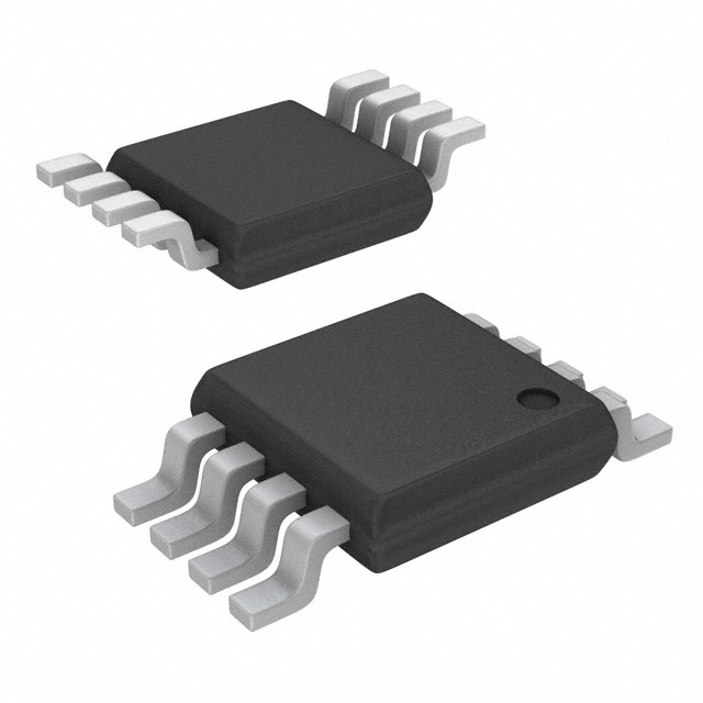
S-89630A
www.ablic.com
125°C OPERATION,
LOW INPUT OFFSET VOLTAGE CMOS OPERATIONAL AMPLIFIER
Rev.1.0_01
© ABLIC Inc., 2018-2019
This IC incorporates a general purpose analog circuit in a small package. This is a zero-drift operational amplifier with
Rail-to-Rail input and output, which uses chopper-stabilizing techniques to provide low input offset voltage.
The S-89630AB is a dual operational amplifier (2 circuits), which is suitable for applications requiring less offset voltage.
Features
• Low input offset voltage:
• Low input offset voltage drift:
• Operation power supply voltage range:
•
•
•
•
•
•
•
•
Low current consumption (Per circuit):
Low input noise voltage:
Low input noise voltage density:
Built-in output current limit circuit:
Internal phase compensation:
Rail-to-Rail input and output
Operation temperature range:
Lead-free (Sn 100%), halogen-free
VIO = +50 μV max. (Ta = −40°C to +125°C)
ΔVIO
= ±25 nV/°C typ. (VDD = 30.0 V, Ta = −40°C to +125°C)
ΔTa
VDD = 4.0 V to 36.0 V (Single supply)
VDD = ±2.0 V to ±18.0 V (Dual supply)
IDD = 250 μA typ.
VNOISE_pp = 0.8 μVpp typ. (f = 0.1 Hz to 10 Hz)
VNOISE = 25 nV/√Hz typ. (f = 1 kHz)
Overcurrent limit when output pin is short-circuited
No external parts required
Ta = −40°C to +125°C
Applications
• High-accuracy current detection
• Various sensor interfaces
• Strain gauge amplifier
Package
• TMSOP-8
1
�125°C OPERATION, LOW INPUT OFFSET VOLTAGE CMOS OPERATIONAL AMPLIFIER
S-89630A
Rev.1.0_01
Block Diagram
VDD
IN1(+)
+
IN1(−)
−
OUT1
IN2(+)
+
IN2(−)
−
OUT2
VSS
Figure 1
2
�125°C OPERATION, LOW INPUT OFFSET VOLTAGE CMOS OPERATIONAL AMPLIFIER
Rev.1.0_01
S-89630A
Product Name Structure
Refer to "1.
Product name" regarding the contents of product name, "2.
drawings and "3.
1.
Package" regarding the package
Product name list" regarding the product type.
Product name
S-89630A B
0
A -
K8T2
U
Environmental code
U:
Lead-free (Sn 100%), halogen-free
Package abbreviation and IC packing specifications*1
K8T2: TMSOP-8, Tape
Operation temperature
A:
Ta = −40°C to +125°C
Number of circuits
B:
2
*1.
2.
Refer to the tape drawing.
Package
Package Name
TMSOP-8
3.
Table 1 Package Drawing Codes
Dimension
Tape
FM008-A-P-SD
Reel
FM008-A-C-SD
FM008-A-R-SD
Product name list
Table 2
Product Name
S-89630AB0A-K8T2U
Package
TMSOP-8
3
�125°C OPERATION, LOW INPUT OFFSET VOLTAGE CMOS OPERATIONAL AMPLIFIER
S-89630A
Rev.1.0_01
Pin Configuration
1.
TMSOP-8
Top view
1
2
3
4
8
7
6
5
Figure 2
4
Pin No.
1
2
3
4
5
6
7
8
Table 3
Symbol
OUT1
IN1(−)
IN1(+)
VSS
IN2(+)
IN2(−)
OUT2
VDD
Description
Output pin 1
Inverted input pin 1
Non-inverted input pin 1
GND pin
Non-inverted input pin 2
Inverted input pin 2
Output pin 2
Positive power supply pin
�125°C OPERATION, LOW INPUT OFFSET VOLTAGE CMOS OPERATIONAL AMPLIFIER
Rev.1.0_01
S-89630A
Absolute Maximum Ratings
Table 4
(Tj = −40°C to +150°C unless otherwise specified)
Item
Power supply voltage
Input voltage
Output voltage
Differential input voltage
Input pin current
Junction temperature
Operation ambient temperature
Storage temperature
Caution
Symbol
VDD
VIN(+), VIN(−)
VOUT
VIND
IIN
Tj
Topr
Tstg
Absolute Maximum Rating
VSS − 0.3 to VSS + 45.0
VSS − 0.3 to VDD + 0.3
VSS − 0.3 to VDD + 0.3
±0.5
±10.0
−40 to +150
−40 to +125
−40 to +150
Unit
V
V
V
V
mA
°C
°C
°C
The absolute maximum ratings are rated values exceeding which the product could suffer
physical damage. These values must therefore not be exceeded under any conditions.
Thermal Resistance Value
Table 5
Item
Symbol
Condition
Board A
Board B
TMSOP-8
θJA
Junction-to-ambient thermal resistance*1
Board C
Board D
Board E
*1. Test environment: compliance with JEDEC STANDARD JESD51-2A
Min.
−
−
−
−
−
Typ.
160
133
−
−
−
Max.
−
−
−
−
−
Unit
°C/W
°C/W
°C/W
°C/W
°C/W
Remark Refer to " Power Dissipation" and "Test Board" for details.
5
�125°C OPERATION, LOW INPUT OFFSET VOLTAGE CMOS OPERATIONAL AMPLIFIER
S-89630A
Rev.1.0_01
Electrical Characteristics
1.
Recommended operation conditions
Table 6
(Ta = −40°C to +125°C unless otherwise specified)
Item
Symbol
Condition
Min.
Typ.
Max.
Unit
Test
Circuit
−
4.0
−
36.0
V
−
Operation power supply
VDD
voltage range
2.
VDD = 5.0 V
Table 7
(Ta = −40°C to +125°C unless otherwise specified)
DC Electrical Characteristics
Item
Symbol
Condition
Min.
Typ.
Max.
Unit
Test
Circuit
VDD
2
−
500
760
μA
5
−50
±10
+50
μV
1
−125
±30
+125
nV/°C
1
Current consumption
(2 circuits)
IDD
VCMR = VOUT =
Input offset voltage
VIO
VCMR =
Input offset voltage drift
ΔVIO
ΔTa
VDD
2
VDD
VCMR = 2
Input bias current
Input offset current
Common-mode
input voltage range
IBIAS
IIO
−
−
−
−
3
3
10
10
nA
nA
9,10
9,10
VCMR
−
VSS
−
VDD
V
2
Voltage gain (open loop)
AVOL
VSS + 0.5 V ≤ VOUT ≤ VDD − 0.5 V,
VDD
VCMR = 2 , RL = 10 kΩ
93
110
−
dB
8
ISOURCE = 100 μA
4.9
−
−
V
3
4.7
−
−
−
V
3
−
0.1
V
4
ISINK = 1 mA
−
−
0.3
V
4
CMRR
VSS ≤ VCMR ≤ VDD
93
110
−
dB
2
PSRR
4.0 V ≤ VDD ≤ 36.0 V
116
130
−
dB
1
Source current
ISOURCE
VOUT = VDD − 0.1 V
0.40
0.60
−
mA
6
Sink current
Output pin short-circuit
current (source)
Output pin short-circuit
current (sink)
ISINK
VOUT = 0.1 V
0.25
0.50
−
mA
7
ISHORT_SOURCE
VOUT = 0 V
−
16.0
−
mA
−
ISHORT_SINK
VOUT = VDD
−
15.0
−
mA
−
Maximum output swing
voltage
Common-mode input
signal rejection ratio
Power supply voltage
rejection ratio
6
VOH
VOL
ISOURCE = 1 mA
ISINK = 100 μA
�125°C OPERATION, LOW INPUT OFFSET VOLTAGE CMOS OPERATIONAL AMPLIFIER
Rev.1.0_01
S-89630A
Table 8
(Ta = −40°C to +125°C unless otherwise specified)
AC Electrical Characteristics
Item
Symbol
Condition
RL = 1.0 MΩ, CL = 15 pF
(Refer to Figure 13 and Figure 14),
VIN(+) = 1.5 V ↔ 3.5 V
CL = 0 pF
Min.
Typ.
Max.
Unit
−
0.45
−
V/μs
Slew rate
SR
Gain-bandwidth product
GBP
−
1.2
−
Maximum load capacitance
CL
−
−
470
−
MHz
pF
Input noise voltage
VNOISE_pp f = 0.1 Hz to 10 Hz
−
0.8
−
μVpp
Input noise voltage density
VNOISE
−
25
−
nV/√Hz
f = 1 kHz
7
�125°C OPERATION, LOW INPUT OFFSET VOLTAGE CMOS OPERATIONAL AMPLIFIER
S-89630A
Rev.1.0_01
3.
VDD = 30.0 V
Table 9
(Ta = −40°C to +125°C unless otherwise specified)
DC Electrical Characteristics
Item
Symbol
Condition
Min.
Typ.
Max.
Unit
Test
Circuit
VDD
2
−
500
760
μA
5
−50
±10
+50
μV
1
−120
±25
+120
nV/°C
1
Current consumption
(2 circuits)
IDD
VCMR = VOUT =
Input offset voltage
VIO
VCMR =
Input offset voltage drift
ΔVIO
ΔTa
Input bias current
IBIAS
−
−
3
10
nA
9,10
Input offset current
Common-mode
input voltage range
IIO
−
−
3
10
nA
9,10
VCMR
−
VSS
−
VDD
V
2
Voltage gain (open loop)
AVOL
VSS + 0.5 V ≤ VOUT ≤ VDD − 0.5 V,
VDD
VCMR = 2 , RL = 10 kΩ
106
120
−
dB
8
ISOURCE = 100 μA
29.9
−
−
V
3
ISOURCE = 1 mA
29.7
−
−
−
V
3
−
0.1
V
4
−
−
0.3
V
4
Maximum output swing
voltage
Common-mode input
signal rejection ratio
Power supply voltage
rejection ratio
VOH
VOL
VDD
2
VDD
VCMR = 2
ISINK = 100 μA
ISINK = 1 mA
CMRR
VSS ≤ VCMR ≤ VDD
106
120
−
dB
2
PSRR
4.0 V ≤ VDD ≤ 36.0 V
116
130
−
dB
1
Source current
ISOURCE
VOUT = VDD − 0.1 V
0.40
0.60
−
mA
6
Sink current
Output pin short-circuit
current (source)
Output pin short-circuit
current (sink)
ISINK
VOUT = 0.1 V
0.25
0.50
−
mA
7
ISHORT_SOURCE
VOUT = 0 V
−
16.0
−
mA
−
ISHORT_SINK
VOUT = VDD
−
15.0
−
mA
−
8
�125°C OPERATION, LOW INPUT OFFSET VOLTAGE CMOS OPERATIONAL AMPLIFIER
Rev.1.0_01
S-89630A
Table 10
(Ta = −40°C to +125°C unless otherwise specified)
AC Electrical Characteristics
Item
Symbol
Slew rate
SR
Gain-bandwidth product
GBP
Maximum load capacitance
CL
Input noise voltage
Input noise voltage density
Condition
RL = 1.0 MΩ, CL = 15 pF
(Refer to Figure 13 and Figure 14),
VIN(+) = 14.0 V ↔ 16.0 V
CL = 0 pF
Min.
Typ.
Max.
Unit
−
0.45
−
V/μs
−
1.2
−
−
470
−
MHz
pF
VNOISE_pp f = 0.1 Hz to 10 Hz
−
0.8
−
μVpp
VNOISE
−
25
−
nV/√Hz
−
f = 1 kHz
9
�125°C OPERATION, LOW INPUT OFFSET VOLTAGE CMOS OPERATIONAL AMPLIFIER
S-89630A
Rev.1.0_01
Test Circuits (Per circuit)
1.
Power supply voltage rejection ratio, input offset voltage, input offset voltage drift
• Power supply voltage rejection ratio (PSRR)
VDD
The power supply voltage rejection ratio (PSRR) can be
calculated by the following expression, with VOUT measured at
each VDD.
RF
RS
−
VOUT
+
RS
Test conditions:
VDD = 4.0 V: VDD = VDD1, VOUT = VOUT1
VDD = 36.0 V: VDD = VDD2, VOUT = VOUT2
RF
PSRR = 20 log
VDD
VCMR = 2
Figure 3
VDD1 − VDD2
VDD1
VDD2
VOUT1 − 2 − VOUT2 − 2
×
RF + RS
RS
• Input offset voltage (VIO)
Test Circuit 1
VIO =
VOUT − VDD
2
×
RS
RF + RS
• Input offset voltage drift
ΔVIO
ΔTa
The input offset voltage drift
ΔVIO
ΔTa
can be calculated by the
following expression, with VOUT measured at each temperature.
Test conditions:
Ta = −40°C: VIO = VIO1
Ta = +125°C: VIO = VIO2
ΔVIO
VIO2 − VIO1
=
ΔTa
+125°C − (−40°C)
2.
Common-mode input signal rejection ratio, common-mode input voltage range
• Common-mode input signal rejection ratio (CMRR)
VDD
The common-mode input signal rejection ratio (CMRR) can be
calculated by the following expression, with VOUT measured at
each VIN.
RF
RS
−
VOUT
+
RS
Test conditions:
VIN = VCMR Max.: VIN = VIN1, VOUT = VOUT1
VIN = VCMR Min.: VIN = VIN2, VOUT = VOUT2
RF
CMRR = 20 log
VIN
VDD
2
Figure 4
10
VIN1 − VIN2
RF + RS
× R
S
VOUT1 − VOUT2
• Common-mode input voltage range (VCMR)
Test Circuit 2
The common-mode input voltage range is the range of VIN in
which VOUT satisfies the common-mode input signal rejection
ratio specifications when VIN is changed.
�125°C OPERATION, LOW INPUT OFFSET VOLTAGE CMOS OPERATIONAL AMPLIFIER
Rev.1.0_01
S-89630A
3.
Maximum output swing voltage
• Maximum output swing voltage (VOH)
VDD
−
VOH
+
Test conditions:
VDD
VIN1 = 2 − 0.1 V
VDD
VIN2 = 2 + 0.1 V
ISOURCE = 100 μA, 1 mA
ISOURCE
VIN1
Figure 5
4.
VDD
2
VIN2
Test Circuit 3
Maximum output swing voltage
VDD
• Maximum output swing voltage (VOL)
VDD
2
Test conditions:
VDD
VIN1 = 2 + 0.1 V
VDD
VIN2 = 2 − 0.1 V
ISINK = 100 μA, 1 mA
ISINK
−
+
VIN1
VIN2
Figure 6
5.
VOL
Test Circuit 4
Current consumption
VDD
• Current consumption (IDD)
A
−
+
VCMR =
VDD
2
Figure 7
Test Circuit 5
11
�125°C OPERATION, LOW INPUT OFFSET VOLTAGE CMOS OPERATIONAL AMPLIFIER
S-89630A
Rev.1.0_01
6.
Source current
• Source current (ISOURCE)
VDD
Test conditions:
VOUT = VDD − 0.1 V
VDD
VIN1 = 2 − 0.1 V
VDD
VIN2 = 2 + 0.1 V
−
+
VIN1
A
VOUT
VIN2
Figure 8
7.
Test Circuit 6
Sink current
VDD
• Sink current (ISINK)
VOUT
Test conditions:
VOUT = 0.1 V
VDD
VIN1 = 2 + 0.1 V
VDD
VIN2 = 2 − 0.1 V
A
−
+
VIN1
VIN2
Figure 9
8.
Test Circuit 7
Voltage gain
• Voltage gain (open loop) (AVOL)
VDD
RS
RF
−
D.U.T
+
RS
RF
VDDN
+
NULL
−
VDD
2
VDD
2
Figure 10
12
VOUT
Test conditions:
VM = VDD − 0.5 V: VM = VM1, VOUT = VOUT1
VM = VSS + 0.5 V: VM = VM2, VOUT = VOUT2
RL
VSSN
VCMR =
The voltage gain (AVOL) can be calculated by the
following expression, with VOUT measured at each
V M.
VM
Test Circuit 8
AVOL = 20 log
RL = 10 kΩ
RF + RS
VM1 − VM2
× R
S
VOUT1 − VOUT2
�125°C OPERATION, LOW INPUT OFFSET VOLTAGE CMOS OPERATIONAL AMPLIFIER
Rev.1.0_01
S-89630A
9.
Input bias current, input offset current
・Input bias current (IBIAS)
VDD
Test conditions:
VDD
−1 × (VOUT − 2 )
IN(+) pin input bias current (IBIAS(+)) =
RB
−
VOUT
+
RB
VDD
VOUT − 2
IN(−) pin input bias current (IBIAS(−)) =
RB
IBIAS =
VCMR =
|IBIAS(+) + IBIAS(−)|
2
VDD
2
・Input offset current (IIO)
Figure 11
Test Circuit 9
IIO = |IBIAS(−) − IBIAS(+)|
VDD
RB
−
VOUT
+
VCMR =
VDD
2
Figure 12
Test Circuit 10
13
�125°C OPERATION, LOW INPUT OFFSET VOLTAGE CMOS OPERATIONAL AMPLIFIER
S-89630A
Rev.1.0_01
10.
Slew rate
VDD
−
VOUT
+
VIN(+)
CL = 15 pF
RL = 1.0 MΩ
VDD
2
Figure 13
Test Circuit 11
tR = tF = 200 ns (10 V/μs)
VDD
2 + 1.0 V
When falling
1.6 V
SR = t
THL
VIN(+)
VDD
2 − 1.0 V
When rising
1.6 V
SR = t
TLH
tTHL
VDD
2 + 1.0 V) × 0.8
VDD
(
2 − 1.0 V) × 0.8
(
VOUT
(= VIN(−))
tTLH
Figure 14
14
・Slew rate (SR)
�125°C OPERATION, LOW INPUT OFFSET VOLTAGE CMOS OPERATIONAL AMPLIFIER
Rev.1.0_01
S-89630A
Precautions
• Generally an operational amplifier may cause oscillation depending on the selection of external parts. Perform
thorough evaluation using the actual application to set the constants.
• Do not apply an electrostatic discharge to this IC that exceeds performance ratings of the built-in electrostatic
protection circuit.
• ABLIC Inc. claims no responsibility for any disputes arising out of or in connection with any infringement by
products including this IC of patents owned by a third party.
• This IC operates stably even directly connecting a load capacitance of 470 pF or less to the output pin, as shown
in Figure 15. When connecting a load capacitance of 470 pF or more, connect a resistor of 100 Ω or more as
shown in Figure 16. In case of connecting a filter for noise prevention, and connecting a load capacitance of
470 pF or more, also connect a resistor of 100 Ω or more as shown in Figure 17.
VDD
VIN+
+
VIN−
−
VOUT
Load
capacitance
470 pF or less
VSS
Figure 15
VDD
VIN+
+
VIN−
−
VOUT
100 Ω or more
Load
capacitance
VSS
Figure 16
VDD
Filter
VIN+
+
VIN−
−
VOUT
100 Ω or more
Load
capacitance
VSS
Figure 17
Caution
The above connection diagrams and constants will not guarantee successful operation.
Perform thorough evaluation using the actual application to set the constants.
15
�125°C OPERATION, LOW INPUT OFFSET VOLTAGE CMOS OPERATIONAL AMPLIFIER
S-89630A
Rev.1.0_01
Precaution for use
1.
Methods for protection against application of overvoltage to input pin
ESD protection elements are connected to the input pins as shown in Figure 1. If the input voltage (VIN) exceeds the
VIN absolute maximum rating VDD + 0.3 V, there is a risk of the input pin current which flows through the ESD
protection element exceeding ±10.0 mA (the absolute maximum rating). In this case, connect a current limiting
resistor (RLIMT) to the input pin as shown in Figure 18 to limit the input pin current to less than ±10.0 mA.
However, error voltage and noise generate as a result of input bias current and input offset current. Select the lowest
possible resistance when connecting the RLIMT.
VDD
VIN
RLIMT
−
+
VOUT
Figure 18
2.
Input voltage range (input crossover distortion)
This IC has two sets of differential circuits in order to achieve the Rail-to-Rail input voltage range. The differential
circuits used switch based on the common-mode input voltage range (VCMR). Differences in the characteristics of the
two sets of differential circuits result in the generation of distortion of the output voltage which is referred to as "input
crossover distortion" when the differential circuits switch.
The differential circuit switching voltage of this IC is approximately between VDD − 2.2 V and VDD − 1.2 V. When using
this IC in applications which require high-accuracy measurement, avoid the range near the differential circuit
switching voltage in order to avoid changes in input offset voltage caused by input crossover distortion and changes
in input offset voltage drift.
This IC is a chopper-stabilized zero-drift amplifier; therefore, it always cancels input offset voltage. For this reason,
the input crossover distortion is kept extremely small when compared to standard operational amplifiers. However,
please contact our sales representatives when using this IC near the differential circuit switching voltage.
Refer to "8. Input offset voltage (VIO) vs. Common-mode input voltage range (VCMR)" in " Characteristics
(Typical Data)".
VDD
Approximately
VDD − 2.2 V to VDD − 1.2 V
Input range
Output
circuit
Differential circuit 1
Differential circuit 2
Figure 19
16
Distortion
�125°C OPERATION, LOW INPUT OFFSET VOLTAGE CMOS OPERATIONAL AMPLIFIER
Rev.1.0_01
S-89630A
3.
Recommended processing methods for unused circuit
When using only a single circuit of this IC, it is recommended that the unused circuit be connected as shown in
Figure 20. Set the non-inverted input pin voltage (VIN(+)) within the common-mode input voltage range (VCMR).
VDD
−
VOUT
+
VIN(+) = VSS to VDD
Figure 20
17
�125°C OPERATION, LOW INPUT OFFSET VOLTAGE CMOS OPERATIONAL AMPLIFIER
S-89630A
Rev.1.0_01
Characteristics (Typical Data)
1.
Current consumption (IDD) (Per circuit) vs. Power supply voltage (VDD)
400
Ta = +125°C
IDD [μA]
300
200
Ta = +25°C
Ta = −40°C
100
0
2.
0
10
20
VDD [V]
30
40
Voltage gain (AVOL) vs. Frequency (f)
VDD = 4.0 V
VDD = 18.0 V
120
120
100
Ta = +125°C
80
60
40
Ta = −40°C
Ta = +25°C
20
0
0.01
0.1
1
10
100
f [kHz]
1000 10000
VDD = 36.0 V
AVOL [dB]
100
Ta = +125°C
80
60
Ta = +25°C
Ta = −40°C
20
0
0.01
18
Ta = +125°C
80
60
40
Ta = +25°C
Ta = −40°C
20
120
40
AVOL [dB]
AVOL [dB]
100
0.1
1
10
100
f [kHz]
1000 10000
0
0.01
0.1
1
10
100
f [kHz]
1000 10000
�125°C OPERATION, LOW INPUT OFFSET VOLTAGE CMOS OPERATIONAL AMPLIFIER
Rev.1.0_01
S-89630A
Output current
3. 1
Source current (ISOURCE) vs. Power supply voltage (VDD)
VOUT = VDD − 0.1 V, VSS = 0 V
1.2
0.8
Ta = −40°C
0.6
Ta = +25°C
ISOURCE [mA]
ISOURCE [mA]
5.0
0.4
Ta = +125°C
0.2
0.0
10
20
VDD [V]
30
3.0
Ta = +25°C
2.0
Ta = +125°C
1.0
40
0
VOUT = VSS + 0.1 V, VSS = 0 V
10
30
40
ISINK [mA]
5.0
0.8
Ta = −40°C
0.6
Ta = +25°C
0.4
0.2
0
10
20
VDD [V]
30
4.0
Ta = −40°C
3.0
Ta = +25°C
2.0
1.0
Ta = +125°C
0.0
Ta = +125°C
0.0
40
0
10
20
VDD [V]
30
40
Output voltage (VOUT) vs. Source current (ISOURCE)
VDD = 4.0 V, VSS = 0 V
VDD = 18.0 V, VSS = 0 V
5.0
20
4.0
Ta = −40°C
3.0
Ta = +25°C
2.0
1.0
Ta = −40°C
Ta = +25°C
15
VOUT [V]
VOUT [V]
20
VDD [V]
VOUT = VSS + 0.5 V, VSS = 0 V
6.0
1.0
ISINK [mA]
Ta = −40°C
Sink current (ISINK) vs. Power supply voltage (VDD)
1.2
3. 3
4.0
0.0
0
3. 2
VOUT = VDD − 0.5 V, VSS = 0 V
6.0
1.0
10
Ta = +125°C
5
Ta = +125°C
0.0
0
0
5
10
15
ISOURCE [mA]
20
25
0
5
10
15
ISOURCE [mA]
20
25
VDD = 36.0 V, VSS = 0 V
40
30
VOUT [V]
3.
Ta = −40°C
20
Ta = +25°C
10
Ta = +125°C
0
0
5
10
15
ISOURCE [mA]
20
25
19
�125°C OPERATION, LOW INPUT OFFSET VOLTAGE CMOS OPERATIONAL AMPLIFIER
S-89630A
Rev.1.0_01
3. 4
Output voltage (VOUT) vs. Sink current (ISINK)
VDD = 18.0 V, VSS = 0 V
VDD = 4.0 V, VSS = 0 V
5.0
Ta = +125°C
4.0
15
VOUT [V]
VOUT [V]
20
3.0
2.0
Ta = +25°C
1.0
0
5
10
15
ISINK [mA]
25
VDD = 36.0 V, VSS = 0 V
VOUT [V]
Ta = +125°C
Ta = +25°C
20
Ta = −40°C
10
0
0
4.
5
10
15
ISINK [mA]
20
25
Input bias current (IBIAS) vs. Temperature (Ta)
VDD = 36.0 V
100
IBIAS [nA]
75
50
25
0
−25
−40 −25
0
25
50
Ta [°C]
20
75
Ta = −40°C
0
20
40
30
Ta = +25°C
10
5
Ta = −40°C
0.0
Ta = +125°C
100
125
0
5
10
15
ISINK [mA]
20
25
�125°C OPERATION, LOW INPUT OFFSET VOLTAGE CMOS OPERATIONAL AMPLIFIER
Rev.1.0_01
S-89630A
5. Input noise voltage density (VNOISE) vs. Frequency (f)
VDD = 4.0 V, VSS = 0 V
Ta = +125°C
Ta = +25°C
10
Ta = −40°C
Ta = +125°C
Ta = +25°C
10
1
Ta = −40°C
1
0.1
1
10
100
f [kHz]
0.1
1
10
100
f [kHz]
VDD = 36.0 V, VSS = 0 V
100
VNOISE [nV/√Hz]
VDD = 18.0 V, VSS = 0 V
100
VNOISE [nV/√Hz]
VNOISE [nV/√Hz]
100
Ta = +125°C
Ta = +25°C
10
Ta = −40°C
1
0.1
1
10
100
f [kHz]
Input pin current (IIN) vs. Differential input voltage (VIND)
VDD = 36.0 V, VSS = 0 V
20
10
IIN [μA]
6.
Ta = −40°C
0
−10
−20
−1.0
Ta = +25°C
Ta = +125°C
−0.5
0.0
VIND [V]
0.5
1.0
21
�125°C OPERATION, LOW INPUT OFFSET VOLTAGE CMOS OPERATIONAL AMPLIFIER
S-89630A
Rev.1.0_01
7.
Input offset voltage (VIO) vs. Power supply voltage (VDD)
VSS = 0 V, VCMR = VDD/2
50
VIO [μV]
25
0
−25
−50
0
20
VDD [V]
30
40
Measured six samples
Remark
8.
10
Input offset voltage (VIO) vs. Common-mode input voltage range (VCMR)
VDD = 4.0 V, VSS = 0 V
VDD = 18.0 V, VSS = 0 V
25
25
VIO [μV]
50
VIO [μV]
50
0
−25
−25
−50
0
1
2
3
4
VCMR [V]
VDD = 36.0 V, VSS = 0 V
50
VIO [μV]
25
0
−25
−50
Remark
22
0
0
10
20
VCMR [V]
Measured four samples
30
40
−50
0
5
10
VCMR [V]
15
20
�125°C OPERATION, LOW INPUT OFFSET VOLTAGE CMOS OPERATIONAL AMPLIFIER
Rev.1.0_01
S-89630A
9.
Voltage gain (open loop) (AVOL) vs. Temperature (Ta)
VDD = 18.0 V, VSS = 0 V
160
140
140
AVOL [dB]
AVOL [dB]
VDD = 4.0 V, VSS = 0 V
160
120
100
80
−40 −25
0
25
50
75
100
125
120
100
80
−40 −25
Ta [°C]
0
25
50
75
100
125
Ta [°C]
VDD = 36.0 V, VSS = 0 V
AVOL [dB]
160
140
120
100
80
−40 −25
0
25
50
75
100
125
Ta [°C]
10.
Power supply voltage rejection ratio (PSRR) vs. Temperature (Ta)
PSRR [dB]
160
140
120
100
80
−40 −25
0
25
50
75
100
125
Ta [°C]
23
�125°C OPERATION, LOW INPUT OFFSET VOLTAGE CMOS OPERATIONAL AMPLIFIER
S-89630A
Rev.1.0_01
11.
Common-mode input signal rejection ratio (CMRR) vs. Temperature (Ta)
140
140
120
100
80
−40 −25
0
25
50
75
100
125
Ta [°C]
VDD = 36.0 V, VSS = 0 V
CMRR [dB]
140
120
100
80
−40 −25
0
25
50
Ta [°C]
120
100
80
−40 −25
0
25
50
Ta [°C]
160
24
VDD = 18.0 V, VSS = 0 V
160
CMRR [dB]
CMRR [dB]
VDD = 4.0 V, VSS = 0 V
160
75
100
125
75
100
125
�125°C OPERATION, LOW INPUT OFFSET VOLTAGE CMOS OPERATIONAL AMPLIFIER
Rev.1.0_01
S-89630A
12.
Step response (Slew rate)
12. 1
Input signal width (0.4 V)
12. 1. 1
VIN(+) = 1.8 V ↔ 2.2 V
12. 1. 2
VIN(+) = 8.8 V ↔ 9.2 V
VDD = 18.0 V, VSS = 0 V
VDD = 4.0 V, VSS = 0 V
9.4
VOUT, Ta = −40°C
2.2
2.0
VIN
1.8
1.6
12. 1. 3
VIN, VOUT [V]
VIN, VOUT [V]
2.4
VOUT, Ta = +125°C
VOUT, Ta = +25°C
−1
0
1
2
3
4
t [μs]
5
6
7
VOUT, Ta = −40°C
9.2
9.0
VIN
8.8
8.6
VOUT, Ta = +125°C
VOUT, Ta = +25°C
−1
0
1
2
3
4
t [μs]
5
6
7
VIN(+) = 17.8 V ↔ 18.2 V
VDD = 36.0 V, VSS = 0 V
VIN, VOUT [V]
18.4
VOUT, Ta = −40°C
18.2
18.0
VIN
17.8
17.6
VOUT, Ta = +125°C
VOUT, Ta = +25°C
−1
0
1
2
3
4
t [μs]
5
6
7
25
�125°C OPERATION, LOW INPUT OFFSET VOLTAGE CMOS OPERATIONAL AMPLIFIER
S-89630A
Rev.1.0_01
12. 2
Input signal width (4.0 V)
12. 2. 1
VIN(+) = 0 V ↔ 4.0 V
VIN(+) = 7.0 V ↔ 11.0 V
12. 2. 2
VDD = 18.0 V, VSS = 0 V
VDD = 4.0 V, VSS = 0 V
5
VOUT, Ta = −40°C
3
2
V IN
1
°
VOUT, Ta = 25°C
0
12. 2. 3
−10
0
10
20
30 40
t [μs]
50
60
VOUT, Ta = −40°C
11
VIN, VOUT [V]
VIN, VOUT [V]
4
−1
12
10
9
V IN
8
°
VOUT, Ta = 25°C
7
6
70
−10
0
10
20
30 40
t [μs]
50
60
70
VIN(+) = 16.0 V ↔ 20.0 V
VDD = 4.0 V, VSS = 0 V
21
VOUT, Ta = −40°C
VIN, VOUT [V]
20
19
18
°
VOUT, Ta = 25°C
16
15
12. 3
V IN
17
−10
0
10
20
30 40
t [μs]
50
60
70
Input signal width (VSS ↔ VDD)
12. 3. 1
VIN(+) = 0 V ↔ 18.0 V
12. 3. 2
VIN(+) = 0 V ↔ 36.0 V
VDD = 36.0 V, VSS = 0 V
40
15
30
10
VIN
VOUT, Ta = −40°C
5
0
−5
26
VIN, VOUT [V]
VIN, VOUT [V]
VDD = 18.0 V, VSS = 0 V
20
VOUT, Ta = 25°C
−10
0
10
20
30 40
t [μs]
50
60
70
20
VIN
10
VOUT, Ta = −40°C
0
−10
VOUT , Ta = +25°C
−20
0
20
40
60 80 100 120 140
t [μs]
�125°C OPERATION, LOW INPUT OFFSET VOLTAGE CMOS OPERATIONAL AMPLIFIER
Rev.1.0_01
S-89630A
13.
Input offset voltage distribution
50
50
40
40
30
20
10
0
30
20
10
0
−50 −40 −30 −20 −10 0 10 20 30 40 50
VIO [μV]
−50 −40 −30 −20 −10 0 10 20 30 40 50
VIO [μV]
Input offset voltage drift distribution
VDD = 5.0 V, VSS = 0 V, Ta = −40°C to +125°C
VDD = 30.0 V, VSS = 0 V, Ta = −40°C to +125°C
50
50
40
40
Percentage [%]
Percentage [%]
14.
VDD = 30.0 V, VSS = 0 V, Ta = +25°C
Percentage [%]
Percentage [%]
VDD = 5.0 V, VSS = 0 V, Ta = +25°C
30
20
10
0
0
20
40 60 80 100 120 140
|ΔVIO/ΔTa| [nV/°C]
30
20
10
0
0
20
40 60 80 100 120 140
|ΔVIO/ΔTa| [nV/°C]
27
�125°C OPERATION, LOW INPUT OFFSET VOLTAGE CMOS OPERATIONAL AMPLIFIER
S-89630A
Rev.1.0_01
Power Dissipation
TMSOP-8
Tj = +150°C max.
1.0
Power dissipation (PD) [W]
B
0.8
A
0.6
0.4
0.2
0.0
0
25
50
75
100
125
150
Ambient temperature (Ta) [°C]
28
Board
Power Dissipation (PD)
A
0.78 W
B
0.94 W
C
−
D
−
E
−
175
�2.90±0.2
8
5
1
4
0.13±0.1
0.2±0.1
0.65±0.1
No. FM008-A-P-SD-1.2
TITLE
TMSOP8-A-PKG Dimensions
No.
FM008-A-P-SD-1.2
ANGLE
UNIT
mm
ABLIC Inc.
�2.00±0.05
4.00±0.1
4.00±0.1
1.00±0.1
+0.1
1.5 -0
1.05±0.05
0.30±0.05
3.25±0.05
4
1
5
8
Feed direction
No. FM008-A-C-SD-2.0
TITLE
TMSOP8-A-Carrier Tape
FM008-A-C-SD-2.0
No.
ANGLE
UNIT
mm
ABLIC Inc.
�16.5max.
13.0±0.3
Enlarged drawing in the central part
13±0.2
(60°)
(60°)
No. FM008-A-R-SD-1.0
TITLE
TMSOP8-A-Reel
No.
FM008-A-R-SD-1.0
QTY.
ANGLE
UNIT
mm
ABLIC Inc.
4,000
�Disclaimers (Handling Precautions)
1.
All the information described herein (product data, specifications, figures, tables, programs, algorithms and
application circuit examples, etc.) is current as of publishing date of this document and is subject to change without
notice.
2.
The circuit examples and the usages described herein are for reference only, and do not guarantee the success of
any specific mass-production design.
ABLIC Inc. is not liable for any losses, damages, claims or demands caused by the reasons other than the products
described herein (hereinafter "the products") or infringement of third-party intellectual property right and any other
right due to the use of the information described herein.
3.
ABLIC Inc. is not liable for any losses, damages, claims or demands caused by the incorrect information described
herein.
4.
Be careful to use the products within their ranges described herein. Pay special attention for use to the absolute
maximum ratings, operation voltage range and electrical characteristics, etc.
ABLIC Inc. is not liable for any losses, damages, claims or demands caused by failures and / or accidents, etc. due to
the use of the products outside their specified ranges.
5.
Before using the products, confirm their applications, and the laws and regulations of the region or country where they
are used and verify suitability, safety and other factors for the intended use.
6.
When exporting the products, comply with the Foreign Exchange and Foreign Trade Act and all other export-related
laws, and follow the required procedures.
7.
The products are strictly prohibited from using, providing or exporting for the purposes of the development of
weapons of mass destruction or military use. ABLIC Inc. is not liable for any losses, damages, claims or demands
caused by any provision or export to the person or entity who intends to develop, manufacture, use or store nuclear,
biological or chemical weapons or missiles, or use any other military purposes.
8.
The products are not designed to be used as part of any device or equipment that may affect the human body, human
life, or assets (such as medical equipment, disaster prevention systems, security systems, combustion control
systems, infrastructure control systems, vehicle equipment, traffic systems, in-vehicle equipment, aviation equipment,
aerospace equipment, and nuclear-related equipment), excluding when specified for in-vehicle use or other uses by
ABLIC, Inc. Do not apply the products to the above listed devices and equipments.
ABLIC Inc. is not liable for any losses, damages, claims or demands caused by unauthorized or unspecified use of
the products.
9.
In general, semiconductor products may fail or malfunction with some probability. The user of the products should
therefore take responsibility to give thorough consideration to safety design including redundancy, fire spread
prevention measures, and malfunction prevention to prevent accidents causing injury or death, fires and social
damage, etc. that may ensue from the products' failure or malfunction.
The entire system in which the products are used must be sufficiently evaluated and judged whether the products are
allowed to apply for the system on customer's own responsibility.
10. The products are not designed to be radiation-proof. The necessary radiation measures should be taken in the
product design by the customer depending on the intended use.
11. The products do not affect human health under normal use. However, they contain chemical substances and heavy
metals and should therefore not be put in the mouth. The fracture surfaces of wafers and chips may be sharp. Be
careful when handling these with the bare hands to prevent injuries, etc.
12. When disposing of the products, comply with the laws and ordinances of the country or region where they are used.
13. The information described herein contains copyright information and know-how of ABLIC Inc. The information
described herein does not convey any license under any intellectual property rights or any other rights belonging to
ABLIC Inc. or a third party. Reproduction or copying of the information from this document or any part of this
document described herein for the purpose of disclosing it to a third-party is strictly prohibited without the express
permission of ABLIC Inc.
14. For more details on the information described herein or any other questions, please contact ABLIC Inc.'s sales
representative.
15. This Disclaimers have been delivered in a text using the Japanese language, which text, despite any translations into
the English language and the Chinese language, shall be controlling.
2.4-2019.07
www.ablic.com
�