S-85S0A Series
5.5 V INPUT, 50 mA SYNCHRONOUS STEP-DOWN
SWITCHING REGULATOR WITH 260 nA QUIESCENT CURRENT
www.ablic.com
www.ablicinc.com
Rev.1.2_00
© ABLIC Inc., 2017-2018
The S-85S0A Series introduces own distinctive low power consumption control and COT (Constant On-Time) control,
features ultra low current consumption (260 nA quiescent current) and fast transient response, operates at PFM control.
The S-85S0A Series realizes high efficiency in a wide range of load current consumption and provides strong support for
extended period operation of mobile devices and wearable devices which are equipped with compact batteries.
The S-85S0A Series can configure a step-down regulator only with a coil, an input capacitor, and an output capacitor. By
using external parts recommended in this datasheet, the occupancy area can be reduced to 1.6 mm × 4.3 mm = 6.9 mm2,
and it contributes to miniaturization of electronic equipment.
Features
Applications
• Ultra low current consumption:
• Efficiency (when under 100 μA load):
• Fast transient response:
• Input voltage:
• Output voltage:
260 nA quiescent current
90.5%
COT control
2.2 V to 5.5 V
0.7 V to 2.5 V, in 0.05 V step
2.6 V to 3.9 V, in 0.1 V step
• Output voltage accuracy:
±1.5% (1.0 V ≤ VOUT ≤ 3.9 V)
±15 mV (0.7 V ≤ VOUT < 1.0 V)
• High side power MOS FET on-resistance:
420 mΩ
• Low side power MOS FET on-resistance:
320 mΩ
• Soft-start function:
1 ms typ.
• Under voltage lockout function (UVLO):
1.8 V typ. (detection voltage)
135°C typ. (detection temperature)
• Thermal shutdown function:
• Overcurrent protection function:
300 mA (at L = 2.2 μH)
• Automatic recovery type short-circuit protection function:Hiccup control
• Input and output capacitors:
Ceramic capacitor compatible
• Operation temperature range:
Ta = −40°C to +85°C
• Lead-free (Sn 100%), halogen-free
Typical Application Circuit
CIN
4.7 F
VIN
SW
PVSS
VOUT
EN
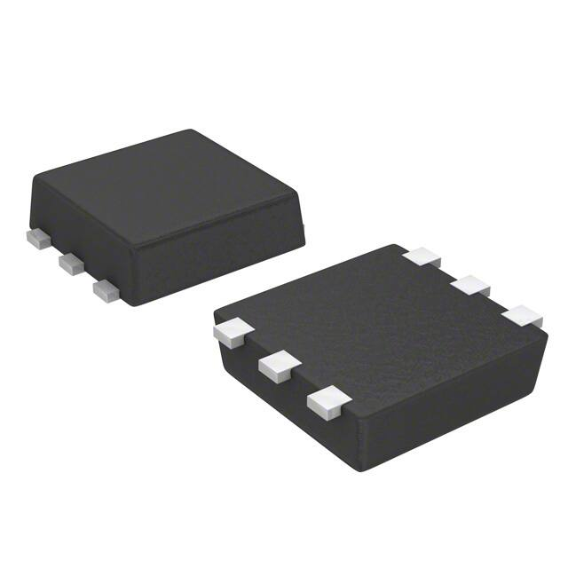
• SNT-6A
(1.80 mm × 1.57 mm × t0.5 mm max.)
VOUT(S) = 1.8 V
100
VOUT
COUT
4.7 F
80
VIN = 2.5 V
60
VIN = 3.6 V
40
VIN = 4.2 V
20
VSS
Package
Efficiency
[%]
VIN
L
2.2 H
• Wearable device
• Bluetooth device
• Wireless sensor network device
• Healthcare equipment
• Smart meter
• Portable game device
0
0.01
0.1
1
IOUT [mA]
10
100
1
�5.5 V INPUT, 50 mA SYNCHRONOUS STEP-DOWN SWITCHING REGULATOR WITH 260 nA QUIESCENT CURRENT
Rev.1.2_00
S-85S0A Series
Block Diagram
CIN
VIN
VIN
VOUT
Error amplifier
−
ON time generation
+
+
circuit
Output control circuit
− UVP circuit
+
Reference voltage circuit
EN
Enable
circuit
Soft-start cicuit
SW
Reverse current
detection circuit
+
−
Thermal shutdown circuit
Overcurrent protection circuit
UVLO circuit
VSS
Figure 1
2
L
PVSS
VOUT
COUT
�5.5 V INPUT, 50 mA SYNCHRONOUS STEP-DOWN SWITCHING REGULATOR WITH 260 nA QUIESCENT CURRENT
Rev.1.2_00
S-85S0A Series
Product Name Structure
Users can select output voltage for the S-85S0A Series. Refer to "1. Product name" regarding the contents of
product name, "2. Package" regarding the package, "3. Product name list" regarding details of the product
name.
1.
Product name
S-85S0A B
xx
-
I6T1
U
Environmental code
U:
Lead-free (Sn 100%), halogen-free
*1
Package name abbreviation and packing specification
I6T1: SNT-6A, Tape
*2, *3
Output voltage
07 to 39
(e.g., when the output voltage is 0.7 V, it is expressed as 07.)
*1.
*2.
*3.
2.
Refer to the tape drawing.
Refer to "3. Product name list".
In the range from 0.7 V to 2.5 V, the products which have 0.05 V step are also available.
Contact our sales office when the product is necessary.
Package
Table 1
Package Name
SNT-6A
Package Drawing Codes
Dimension
Tape
Reel
Land
PG006-A-P-SD
PG006-A-C-SD
PG006-A-R-SD
PG006-A-L-SD
3
�5.5 V INPUT, 50 mA SYNCHRONOUS STEP-DOWN SWITCHING REGULATOR WITH 260 nA QUIESCENT CURRENT
Rev.1.2_00
S-85S0A Series
3.
Product name list
Table 2
Output Voltage (VOUT)
0.7 V ± 15 mV
0.8 V ± 15 mV
0.9 V ± 15 mV
1.0 V ± 1.5%
1.1 V ± 1.5%
1.2 V ± 1.5%
1.3 V ± 1.5%
1.4 V ± 1.5%
1.5 V ± 1.5%
1.6 V ± 1.5%
1.7 V ± 1.5%
1.8 V ± 1.5%
1.9 V ± 1.5%
2.0 V ± 1.5%
2.1 V ± 1.5%
2.2 V ± 1.5%
2.3 V ± 1.5%
2.4 V ± 1.5%
2.5 V ± 1.5%
2.6 V ± 1.5%
2.7 V ± 1.5%
2.8 V ± 1.5%
2.9 V ± 1.5%
3.0 V ± 1.5%
3.1 V ± 1.5%
3.2 V ± 1.5%
3.3 V ± 1.5%
3.4 V ± 1.5%
3.5 V ± 1.5%
3.6 V ± 1.5%
3.7 V ± 1.5%
3.8 V ± 1.5%
3.9 V ± 1.5%
Remark
4
S-85S0A Series
S-85S0AB07-I6T1U
S-85S0AB08-I6T1U
S-85S0AB09-I6T1U
S-85S0AB10-I6T1U
S-85S0AB11-I6T1U
S-85S0AB12-I6T1U
S-85S0AB13-I6T1U
S-85S0AB14-I6T1U
S-85S0AB15-I6T1U
S-85S0AB16-I6T1U
S-85S0AB17-I6T1U
S-85S0AB18-I6T1U
S-85S0AB19-I6T1U
S-85S0AB20-I6T1U
S-85S0AB21-I6T1U
S-85S0AB22-I6T1U
S-85S0AB23-I6T1U
S-85S0AB24-I6T1U
S-85S0AB25-I6T1U
S-85S0AB26-I6T1U
S-85S0AB27-I6T1U
S-85S0AB28-I6T1U
S-85S0AB29-I6T1U
S-85S0AB30-I6T1U
S-85S0AB31-I6T1U
S-85S0AB32-I6T1U
S-85S0AB33-I6T1U
S-85S0AB34-I6T1U
S-85S0AB35-I6T1U
S-85S0AB36-I6T1U
S-85S0AB37-I6T1U
S-85S0AB38-I6T1U
S-85S0AB39-I6T1U
Please contact our sales office for products with specifications other than the above.
�5.5 V INPUT, 50 mA SYNCHRONOUS STEP-DOWN SWITCHING REGULATOR WITH 260 nA QUIESCENT CURRENT
Rev.1.2_00
S-85S0A Series
Pin Configuration
1.
SNT-6A
Table 3
Top view
1
2
3
Pin No.
6
5
4
Figure 2
Symbol
1
2
3
4
5
VOUT
VSS
SW
PVSS
VIN
6
EN
Description
Voltage output pin
GND pin
External inductor connection pin
Power GND pin
Power supply pin
Enable pin
"H"
: Enable (normal operation)
"L"
: Disable (standby)
5
�5.5 V INPUT, 50 mA SYNCHRONOUS STEP-DOWN SWITCHING REGULATOR WITH 260 nA QUIESCENT CURRENT
Rev.1.2_00
S-85S0A Series
Absolute Maximum Ratings
Table 4
(Unless otherwise specified: Ta = +25°C, VSS = 0 V)
Item
VIN pin voltage
EN pin voltage
VOUT pin voltage
SW pin voltage
PVSS pin voltage
Operation temperature
Storage temperature
Symbol
VIN
VEN
VOUT
VSW
VPVSS
Topr
Tstg
Absolute Maximum Rating
Unit
VSS − 0.3 to VSS + 6.0
VSS − 0.3 to VIN + 0.3 ≤ VSS + 6.0
VSS − 0.3 to VIN + 0.3 ≤ VSS + 6.0
VSS − 0.3 to VIN + 0.3 ≤ VSS + 6.0
VSS − 0.3 to VSS + 0.3 ≤ VSS + 6.0
−40 to +85
−40 to +125
V
V
V
V
V
°C
°C
Caution The absolute maximum ratings are rated values exceeding which the product could suffer physical
damage. These values must therefore not be exceeded under any conditions.
Thermal Resistance Value
Table 5
Item
Symbol
Condition
Board A
Board B
Junction-to-ambient thermal resistance*1 θJA
SNT-6A
Board C
Board D
Board E
*1. Test environment: compliance with JEDEC STANDARD JESD51-2A
Remark Refer to " Power Dissipation" and "Test Board" for details.
6
Min.
−
−
−
−
−
Typ.
224
176
−
−
−
Max.
−
−
−
−
−
Unit
°C/W
°C/W
°C/W
°C/W
°C/W
�5.5 V INPUT, 50 mA SYNCHRONOUS STEP-DOWN SWITCHING REGULATOR WITH 260 nA QUIESCENT CURRENT
Rev.1.2_00
S-85S0A Series
Electrical Characteristics
Table 6
(VIN = 3.6 V*1, Ta = +25°C unless otherwise specified)
Item
Operating input voltage
Output voltage*2
Symbol
VIN
Condition
Min.
Typ.
Max.
Unit
−
2.2
VOUT(S)
× 0.985
VOUT(S)
− 0.015
3.6
5.5
VOUT(S)
× 1.015
VOUT(S)
+ 0.015
V
1.0 V ≤ VOUT ≤ 3.9 V, no external parts
VOUT
0.7 V ≤ VOUT 2.5 V)
Table 11
Manufacturer
Part Number
Capacitance
Withstanding
Voltage
Dimensions (L × W × H)
Murata Manufacturing Co., Ltd.
TDK Corporation
GRJ155R61A106ME12
C1005X5R0J106M050BC
10 μF
10 μF
10 V
6.3 V
1.0 mm × 0.5 mm × 0.5 mm
1.0 mm × 0.5 mm × 0.5 mm
3.
Inductor (L)
When selecting L, note the allowable current. If a current exceeding this allowable current flows through the inductor,
magnetic saturation may occur, and there may be risks which substantially lower efficiency and damage the IC as a
result of large current.
Therefore, select an inductor so that peak current value (IPK), even during overcurrent detection, does not exceed
the allowable current.
When prioritizing the load response, select an inductor with a small L value such as 2.2 μH. When prioritizing the
efficiency, select an inductor with a large L value such as 4.7 μH. IPK is calculated using the following expression.
IPK = IOUT +
1
(VIN − VOUT) × VOUT
×
VIN
2 × L × fSW
Recommended Inductors (L) List (at VIN ≤ 4.2 V)
Rated
Part Number
Inductance
Dimensions (L × W × H)
Current
MBKK1608T2R2M
520 mA
2.2 μH
1.6 mm × 0.8 mm × 1.0 mm
2000 mA 2.0 mm × 1.2 mm × 1.0 mm
DFE201210S-2R2M=P2
2.2 μH
74438313022
850 mA
2.2 μH
1.6 mm × 1.6 mm × 1.0 mm
MLP2012S2R2MT0S1
800 mA
2.2 μH
2.0 mm × 1.25 mm × 0.85 mm
Table 12
Manufacturer
TAIYO YUDEN CO.,LTD.
Murata Manufacturing Co., Ltd.
Würth Elektronik GmbH & Co. KG
TDK Corporation
Recommended Inductors (L) List (at VIN > 4.2 V)
Rated
Part Number
Inductance
Dimensions (L × W × H)
Current
DFE201210S-2R2M=P2
2000 mA 2.0 mm × 1.2 mm × 1.0 mm
2.2 μH
74438313022
850 mA
2.2 μH
1.6 mm × 1.6 mm × 1.0 mm
MLP2012S2R2MT0S1
800 mA
2.2 μH
2.0 mm × 1.25 mm × 0.85 mm
Table 13
Manufacturer
Murata Manufacturing Co., Ltd.
Würth Elektronik GmbH & Co. KG
TDK Corporation
13
�5.5 V INPUT, 50 mA SYNCHRONOUS STEP-DOWN SWITCHING REGULATOR WITH 260 nA QUIESCENT CURRENT
Rev.1.2_00
S-85S0A Series
Board Layout Guidelines
Note the following cautions when determining the board layout for the S-85S0A Series.
• Place CIN as close to the VIN pin and the PVSS pin as possible.
• Make the VIN pattern and GND pattern as wide as possible.
• Place thermal vias in the GND pattern to ensure sufficient heat dissipation.
• Keep thermal vias near CIN and COUT approximately 3 mm to 4 mm away from capacitor pins.
• Large current flows through the SW pin. Make the wiring area of the pattern to be connected to the SW pin small to
minimize parasitic capacitance and emission noise.
• Do not wire the SW pin pattern under the IC.
Total size
Figure 8
1.6 mm × 4.3 mm = 6.9 mm2
Reference Board Pattern
Caution The above pattern diagram does not guarantee successful operation. Perform thorough evaluation
using the actual application to determine the pattern.
Remark
14
Refer to the land drawing of SNT-6A and "SNT Package User's Guide".
�5.5 V INPUT, 50 mA SYNCHRONOUS STEP-DOWN SWITCHING REGULATOR WITH 260 nA QUIESCENT CURRENT
Rev.1.2_00
S-85S0A Series
Precautions
•
Mount external capacitors and inductors as close as possible to the IC, and make single GND.
•
Characteristic ripple voltage and spike noise occur in the IC containing switching regulators. Moreover rush current
flows at the time of a power supply injection. Because these largely depend on the inductor, the capacitor and
impedance of power supply to be used, fully check them using an actually mounted model.
•
The 4.7 μF capacitor connected between the VIN pin and the VSS pin is a bypass capacitor. It stabilizes the power
supply in the IC, and thus effectively works for stable switching regulator operation. Allocate the bypass capacitor
as close to the IC as possible, prioritized over other parts.
•
Although the IC contains a static electricity protection circuit, static electricity or voltage that exceeds the limit of
the protection circuit should not be applied.
•
The power dissipation of the IC greatly varies depending on the size and material of the board to be connected.
Perform sufficient evaluation using an actual application before designing.
•
ABLIC Inc. assumes no responsibility for the way in which this IC is used on products created using this IC or for
the specifications of that product, nor does ABLIC Inc. assume any responsibility for any infringement of patents or
copyrights by products that include this IC either in Japan or in other countries.
15
�5.5 V INPUT, 50 mA SYNCHRONOUS STEP-DOWN SWITCHING REGULATOR WITH 260 nA QUIESCENT CURRENT
Rev.1.2_00
S-85S0A Series
Characteristics (Typical Data)
Example of major power supply dependence characteristics (Ta = +25°C)
ISS1 [nA]
1. 1
Current consumption during switching off (ISS1)
vs. Input voltage (VIN)
1. 2
100
400
80
300
200
100
40
0
2.0
2.5
3.0
3.5 4.0
VIN [V]
4.5
5.0
5.5
1. 3
Output voltage (VOUT) vs. Input voltage (VIN)
VOUT(S) = 1.2 V
1.230
2.0
1. 4
1.220
2.5
3.0
3.5 4.0
VIN [V]
4.5
5.0
5.5
Output voltage (VOUT) vs. Input voltage (VIN)
VOUT(S) = 1.8 V
1.840
1.820
VOUT [V]
1.210
1.200
1.190
1.800
1.780
1.180
1.170
60
20
0
VOUT [V]
Current consumption during shutdown (ISSS)
vs. Input voltage (VIN)
500
ISSS [nA]
1.
1.760
2.0
2.5
3.0
3.5 4.0
VIN [V]
4.5
5.0
5.5
2.0
2.5
3.0
3.5 4.0
VIN [V]
4.5
5.0
5.5
1. 5
Output voltage (VOUT) vs. Input voltage (VIN)
VOUT(S) = 2.5 V
2.600
VOUT [V]
2.400
2.200
2.000
1.800
2.0
1. 6
2.5
3.0
3.5 4.0
VIN [V]
4.5
5.0
5.5
ON time (tON) vs. Input voltage (VIN)
VOUT(S) = 1.8 V
1.0
1. 7
fSW [MHz]
tON [s]
0.8
0.6
0.4
0.2
1.2
1.0
0.8
0.6
0.0
2.0
16
Switching frequency (fSW) vs. Input voltage (VIN)
VOUT(S) = 1.8 V
1.4
2.5
3.0
3.5 4.0
VIN [V]
4.5
5.0
5.5
2.0
2.5
3.0
3.5 4.0
VIN [V]
4.5
5.0
5.5
�5.5 V INPUT, 50 mA SYNCHRONOUS STEP-DOWN SWITCHING REGULATOR WITH 260 nA QUIESCENT CURRENT
Rev.1.2_00
S-85S0A Series
Soft-start wait time (tSSW) vs. Input voltage (VIN)
1. 9
2.50
2.00
2.00
1.50
1.00
0.50
3.0
3.5 4.0
VIN [V]
4.5
5.0
5.5
2.0
800
700
600
500
400
300
200
100
0
RHFET [m]
RHFET [m]
2.5
High side power MOS FET on-resistance (RHFET) 1. 11
vs. Input voltage (VIN)
2.0
2.5
3.0
3.5 4.0
VIN [V]
4.5
5.0
2.0
80
ILSW [nA]
80
20
4.5
5.0
5.5
2.5
3.0
3.5 4.0
VIN [V]
4.5
5.0
5.5
60
40
20
0
0
2.0
2.5
3.0
3.5 4.0
VIN [V]
4.5
5.0
5.5
1. 14 High level input voltage (VSH) vs. Input voltage (VIN)
2.0
1.0
1.0
0.8
0.8
VSL [V]
1.2
0.6
0.4
0.2
2.5
3.0
3.5 4.0
VIN [V]
4.5
5.0
5.5
1. 15 Low level input voltage (VSL) vs. Input voltage (VIN)
1.2
0.0
3.5 4.0
VIN [V]
1. 13 Low side power MOS FET leakage current (ILSW)
vs. Input voltage (VIN)
100
40
3.0
800
700
600
500
400
300
200
100
0
100
60
2.5
Low side power MOS FET on-resistance (RLFET)
vs. Input voltage (VIN)
5.5
1. 12 High side power MOS FET leakage current (IHSW)
vs. Input voltage (VIN)
IHSW [nA]
1.00
0.00
2.0
1. 10
1.50
0.50
0.00
VSH [V]
Soft-start time (tSS) vs. Input voltage (VIN)
2.50
tSS [ms]
tSSW [ms]
1. 8
0.6
0.4
0.2
2.0
2.5
3.0
3.5 4.0
VIN [V]
4.5
5.0
5.5
0.0
2.0
2.5
3.0
3.5 4.0
VIN [V]
4.5
5.0
5.5
17
�5.5 V INPUT, 50 mA SYNCHRONOUS STEP-DOWN SWITCHING REGULATOR WITH 260 nA QUIESCENT CURRENT
Rev.1.2_00
S-85S0A Series
2.
Example of major temperature characteristics (Ta = −40°C to +85°C)
2. 1
Current consumption during switching off (ISS1)
vs. Temperature (Ta)
2. 2
500
200
VDD = 5.5 V
VDD = 2.2 V
300
200
VDD = 3.6 V
100
2. 3
−40 −25
150
ISSS [nA]
ISS1 [nA]
400
0
Current consumption during shutdown (ISSS)
vs. Temperature (Ta)
VDD = 2.2 V
100
25
Ta [C]
50
75 85
Output voltage (VOUT) vs. Temperature (Ta)
VDD = 5.5 V
50
0
0
VDD = 3.6 V
2. 4
−40 −25
0
25
Ta [C]
VOUT(S) = 1.8 V
1.840
1.210
1.200
1.190
VDD = 3.6 V
2. 5
−40 −25
1.800
1.760
0
25
Ta [C]
50
VDD = 5.5 V
1.780
1.180
1.170
VDD = 2.2 V
VDD = 3.6 V
1.820
VOUT [V]
VOUT [V]
VDD = 2.2 V
VDD = 5.5 V
75 85
Output voltage (VOUT) vs. Temperature (Ta)
VOUT(S) = 1.2 V
1.230
1.220
50
75 85
−40 −25
0
25
Ta [C]
50
75 85
Output voltage (VOUT) vs. Temperature (Ta)
VOUT(S) = 2.5 V
2.560
VOUT [V]
2.540
VDD = 5.5 V
2.520
2.500
2.480
VDD = 3.6 V
2.460
2.440
2. 6
40 25
0
25
Ta [C]
50
75 85
ON time (tON) vs. Temperature (Ta)
2. 7
1.2
1.4
0.8
VDD = 3.6 V
0.6
VDD = 2.2 V
0.4
0.2
18
fSW [MHz]
tON [s]
1.0
0.0
Switching frequency (fSW) vs. Temperature (Ta)
VDD = 5.5 V
−40 −25
0
25
Ta [C]
1.2
1.0
0.8
0.6
50
75 85
VDD = 3.6 V
VDD = 5.5 V
−40 −25
0
VDD = 2.2 V
25
Ta [C]
50
75 85
�5.5 V INPUT, 50 mA SYNCHRONOUS STEP-DOWN SWITCHING REGULATOR WITH 260 nA QUIESCENT CURRENT
Rev.1.2_00
S-85S0A Series
Soft-start wait time (tSSW) vs. Temperature (Ta)
2.00
2.00
1.50
VDD = 5.5 V
1.00
VDD = 3.6 V
40 25
VDD = 2.2 V
25
Ta [C]
50
2. 11
RLFET [m]
RHFET [m]
0.50
VDD = 2.2 V
VDD = 5.5 V
40
25
1.00
75 85
VDD = 3.6 V
0
25
Ta [C]
50
250
200
200
100
50
0
−40 −25
0
25
Ta [C]
50
0.6
0.2
0.0
VDD = 2.2 V
−40 −25
VDD = 3.6 V
25
Ta [C]
25
0
VDD = 3.6 V
25
Ta [C]
50
75 85
VDD = 5.5 V
VDD = 3.6 V
100
VDD = 2.2 V
50
0
25
Ta [C]
50
75 85
VDD = 5.5 V
1.0
0.8
0.6
0.4
0.2
75 85
−40 −25
1.2
0.0
0
75 85
2. 15 Low level input voltage (VSL) vs. Temperature (Ta)
VSL [V]
0.8
0.4
VDD = 5.5 V
150
0
75 85
VDD = 5.5 V
1.0
50
50
2. 14 High level input voltage (VSH) vs. Temperature (Ta)
1.2
25
Ta [C]
2. 13 Low side power MOS FET leakage current (ILSW)
vs. Temperature (Ta)
250
VDD = 5.5 V
0
VDD = 2.2 V
40
300
VDD = 3.6 V
VDD = 2.2 V
40 25
800
700
600
500
400
300
200
100
0
300
150
VDD = 3.6 V
VDD = 5.5 V
Low side power MOS FET on-resistance (RLFET)
vs. Temperature (Ta)
75 85
2. 12 High side power MOS FET leakage current (IHSW)
vs. Temperature (Ta)
VDD = 2.2 V
1.50
0.00
0
2. 10 High side power MOS FET on-resistance (RHFET)
vs. Temperature (Ta)
800
700
600
500
400
300
200
100
0
tSS [ms]
2.50
0.00
IHSW [nA]
Soft-start time (tSS) vs. Temperature (Ta)
2.50
0.50
VSH [V]
2. 9
ILSW [nA]
tSSW [ms]
2. 8
VDD = 2.2 V
40 25
0
VDD = 3.6 V
25
Ta [C]
50
75 85
19
�5.5 V INPUT, 50 mA SYNCHRONOUS STEP-DOWN SWITCHING REGULATOR WITH 260 nA QUIESCENT CURRENT
Rev.1.2_00
S-85S0A Series
2.2
2.2
2.1
2.1
2.0
2.0
1.9
1.8
1.7
1.6
20
2. 17 UVLO release voltage (VUVLO+) vs. Temperature (Ta)
VUVLO [V]
VUVLO [V]
2. 16 UVLO detection voltage (VUVLO−) vs. Temperature (Ta)
1.9
1.8
1.7
40 25
0
25
Ta [C]
50
75 85
1.6
40 25
0
25
Ta [C]
50
75 85
�5.5 V INPUT, 50 mA SYNCHRONOUS STEP-DOWN SWITCHING REGULATOR WITH 260 nA QUIESCENT CURRENT
Rev.1.2_00
S-85S0A Series
Transient response characteristics
The external parts shown in Table 14 are used in "3.
Transient response characteristics".
Table 14
Element Name
Inductor
Input capacitor
Output capacitor
Part Number
DFE201210S-2R2M=P2
C1005X5R0J106M050BC
C1005X5R0J106M050BC
Power-on (VOUT = 1.8 V, VIN = 0 V → 3.6 V, Ta = +25°C)
4
5
3. 1. 2
4
3
2
1
0
−1
−2
−3
−4
IOUT = 50 mA
VIN
VOUT
IL
0
1
2
3
Time [ms]
4
1,400
1,200
1,000
800
600
400
200
0
−200
IL [mA]
1,400
1,200
1,000
800
600
400
200
0
−200
VIN [V], VOUT [V]
3. 1. 1 IOUT = 0.1 mA
4
3
2
1
0
−1
−2
−3
−4
0
1
2
3
Time [ms]
3. 2
Manufacturer
Murata Manufacturing Co., Ltd.
TDK Corporation
TDK Corporation
IL [mA]
VIN [V], VOUT [V]
3. 1
Constant
2.2 μH
10 μF
10 μF
5
Transient response characteristics of EN pin
IL
4
5
IOUT = 50 mA
VEN
IL [mA]
VOUT
IL
0
1
2
3
Time [ms]
4
1,400
1,200
1,000
800
600
400
200
0
−200
5
Power supply fluctuation (VOUT = 1.8 V, Ta = +25°C)
IOUT = 0.1 mA
5
3. 3. 2
VIN = 3.6 V → 4.2 V → 3.6 V
2.10
5
4
4
VIN
2.00
3
VOUT
1.90
2
1
0
10
20
30
Time [ms]
40
50
IOUT = 50 mA
VIN = 3.6 V → 4.2 V → 3.6 V
2.10
3
1.80
2
1.70
1
2.00
VIN
VOUT
1.90
VOUT [V]
3. 3. 1
VIN [V]
VOUT
3. 2. 2
4
3
2
1
0
−1
−2
−3
−4
VIN [V]
3. 3
VEN
1,400
1,200
1,000
800
600
400
200
0
−200
VEN [V], VOUT [V]
3. 2. 1 IOUT = 0.1 mA
4
3
2
1
0
−1
−2
−3
−4
0
1
2
3
Time [ms]
IL [mA]
VEN [V], VOUT [V]
(VOUT = 1.8 V, VIN = 3.6 V, VEN = 0 V → 3.6 V, Ta = +25°C)
VOUT [V]
3.
1.80
1.70
0
10
20
30
Time [ms]
40
50
21
�5.5 V INPUT, 50 mA SYNCHRONOUS STEP-DOWN SWITCHING REGULATOR WITH 260 nA QUIESCENT CURRENT
Rev.1.2_00
S-85S0A Series
Load fluctuation (VOUT = 1.8 V, VIN = 3.6 V, Ta = +25°C)
50
IOUT [mA]
0
IOUT
−50
3. 4. 2
100
1.95
50
1.90
0
1.85
−100
1.80
VOUT
−150
−200
2.00
0
10
20
Time [ms]
30
2.00
1.95
IOUT
−50
−100
1.75
−150
1.70
−200
40
IOUT = 0.1 mA → 50 mA → 0.1 mA
1.90
1.85
1.80
VOUT 1.75
0
10
20
Time [ms]
VOUT [V]
IOUT = 0.1 mA → 10 mA → 0.1 mA
IOUT [mA]
3. 4. 1
100
VOUT [V]
3. 4
1.70
40
30
Reference Data
The external parts shown in Table 15 are used in " Reference Data".
Table 15
Condition
η [%]
1. 1
Efficiency (η) vs. Output current (IOUT)
1. 2
1.5
80
1.4
60
40
0
0.001
VIN = 3.6 V
VIN = 5.5 V
VIN = 3.6 V
1.3
1.2
1.1
0.01
0.1
1
IOUT [mA]
10
1.0
0.001
100
VIN = 5.5 V
0.01
0.1
1
IOUT [mA]
10
100
VOUT = 1.8 V (External parts: Condition)
Efficiency (η) vs. Output current (IOUT)
2. 2
Output voltage (VOUT) vs. Output current (IOUT)
100
2.0
80
1.9
60
40
VOUT [V]
η [%]
2. 1
VIN = 3.6 V
VIN = 5.5 V
20
0
0.001
22
Output voltage (VOUT) vs. Output current (IOUT)
100
20
2.
Output Capacitor (COUT)
GRM035R60J475ME15 (4.7 μF)
Murata Manufacturing Co., Ltd.
C1005X5R0J106M050BC (10 μF)
TDK Corporation
VOUT = 1.2 V (External parts: Condition)
VOUT [V]
1.
Input Capacitor (CIN)
GRM035R60J475ME15 (4.7 μF)
Murata Manufacturing Co., Ltd.
C1005X5R0J106M050BC (10 μF)
TDK Corporation
Inductor (L)
MBKK1608T2R2M (2.2 μH)
TAIYO YUDEN CO.,LTD.
DFE201210S-2R2M=P2 (2.2 μH)
Murata Manufacturing Co., Ltd.
VIN = 3.6 V
1.8
1.7
VIN = 5.5 V
1.6
0.01
0.1
1
IOUT [mA]
10
100
1.5
0.001
0.01
0.1
1
IOUT [mA]
10
100
�5.5 V INPUT, 50 mA SYNCHRONOUS STEP-DOWN SWITCHING REGULATOR WITH 260 nA QUIESCENT CURRENT
Rev.1.2_00
S-85S0A Series
VOUT = 1.2 V (External parts: Condition)
η [%]
3. 1
Efficiency (η) vs. Output current (IOUT)
3. 2
1.5
80
1.4
60
40
VIN = 3.6 V
VIN = 5.5 V
20
0
0.001
VIN = 5.5 V
1.3
1.2
1.1
0.01
0.1
1
IOUT [mA]
10
1.0
0.001
100
VIN = 3.6 V
0.01
0.1
1
IOUT [mA]
10
100
VOUT = 1.8 V (External parts: Condition)
Efficiency (η) vs. Output current (IOUT)
4. 2
Output voltage (VOUT) vs. Output current (IOUT)
100
2.0
80
1.9
60
40
VOUT [V]
4. 1
η [%]
4.
Output voltage (VOUT) vs. Output current (IOUT)
100
VOUT [V]
3.
VIN = 3.6 V
VIN = 5.5 V
20
0
0.001
VIN = 5.5 V
1.8
1.7
VIN = 3.6 V
1.6
0.01
0.1
1
IOUT [mA]
10
100
1.5
0.001
0.01
0.1
1
IOUT [mA]
10
100
23
�5.5 V INPUT, 50 mA SYNCHRONOUS STEP-DOWN SWITCHING REGULATOR WITH 260 nA QUIESCENT CURRENT
Rev.1.2_00
S-85S0A Series
Power Dissipation
SNT-6A
Tj = 125C max.
Power dissipation (PD) [W]
1.0
0.8
B
0.6
A
0.4
0.2
0.0
0
25
50
75
100
125
150
Ambient temperature (Ta) [C]
24
Board
Power Dissipation (PD)
A
0.45 W
B
C
0.57 W
−
D
−
E
−
175
�SNT-6A Test Board
(1) Board A
IC Mount Area
Item
Size [mm]
Material
Number of copper foil layer
Copper foil layer [mm]
1
2
3
4
Thermal via
Specification
114.3 x 76.2 x t1.6
FR-4
2
Land pattern and wiring for testing: t0.070
74.2 x 74.2 x t0.070
-
(2) Board B
Item
Size [mm]
Material
Number of copper foil layer
Copper foil layer [mm]
Thermal via
1
2
3
4
Specification
114.3 x 76.2 x t1.6
FR-4
4
Land pattern and wiring for testing: t0.070
74.2 x 74.2 x t0.035
74.2 x 74.2 x t0.035
74.2 x 74.2 x t0.070
-
No. SNT6A-A-Board-SD-1.0
ABLIC Inc.
�1.57±0.03
6
1
5
4
2
3
+0.05
0.08 -0.02
0.5
0.48±0.02
0.2±0.05
No. PG006-A-P-SD-2.1
TITLE
SNT-6A-A-PKG Dimensions
No.
PG006-A-P-SD-2.1
ANGLE
UNIT
mm
ABLIC Inc.
�+0.1
ø1.5 -0
4.0±0.1
2.0±0.05
0.25±0.05
+0.1
1.85±0.05
ø0.5 -0
4.0±0.1
0.65±0.05
3 2 1
4
5 6
Feed direction
No. PG006-A-C-SD-2.0
TITLE
SNT-6A-A-Carrier Tape
No.
PG006-A-C-SD-2.0
ANGLE
UNIT
mm
ABLIC Inc.
�12.5max.
9.0±0.3
Enlarged drawing in the central part
ø13±0.2
(60°)
(60°)
No. PG006-A-R-SD-1.0
SNT-6A-A-Reel
TITLE
No.
PG006-A-R-SD-1.0
ANGLE
QTY.
UNIT
mm
ABLIC Inc.
5,000
�0.52
1.36
2
0.52
0.2 0.3
1.
2.
1
(0.25 mm min. / 0.30 mm typ.)
(1.30 mm ~ 1.40 mm)
0.03 mm
SNT
1. Pay attention to the land pattern width (0.25 mm min. / 0.30 mm typ.).
2. Do not widen the land pattern to the center of the package ( 1.30 mm ~ 1.40 mm ).
Caution 1. Do not do silkscreen printing and solder printing under the mold resin of the package.
2. The thickness of the solder resist on the wire pattern under the package should be 0.03 mm
or less from the land pattern surface.
3. Match the mask aperture size and aperture position with the land pattern.
4. Refer to "SNT Package User's Guide" for details.
1.
2.
(0.25 mm min. / 0.30 mm typ.)
(1.30 mm ~ 1.40 mm)
No. PG006-A-L-SD-4.1
TITLE
SNT-6A-A
-Land Recommendation
No.
PG006-A-L-SD-4.1
ANGLE
UNIT
mm
ABLIC Inc.
�Disclaimers (Handling Precautions)
1.
All the information described herein (product data, specifications, figures, tables, programs, algorithms and
application circuit examples, etc.) is current as of publishing date of this document and is subject to change without
notice.
2.
The circuit examples and the usages described herein are for reference only, and do not guarantee the success of
any specific mass-production design.
ABLIC Inc. is not liable for any losses, damages, claims or demands caused by the reasons other than the products
described herein (hereinafter "the products") or infringement of third-party intellectual property right and any other
right due to the use of the information described herein.
3.
ABLIC Inc. is not liable for any losses, damages, claims or demands caused by the incorrect information described
herein.
4.
Be careful to use the products within their ranges described herein. Pay special attention for use to the absolute
maximum ratings, operation voltage range and electrical characteristics, etc.
ABLIC Inc. is not liable for any losses, damages, claims or demands caused by failures and / or accidents, etc. due to
the use of the products outside their specified ranges.
5.
Before using the products, confirm their applications, and the laws and regulations of the region or country where they
are used and verify suitability, safety and other factors for the intended use.
6.
When exporting the products, comply with the Foreign Exchange and Foreign Trade Act and all other export-related
laws, and follow the required procedures.
7.
The products are strictly prohibited from using, providing or exporting for the purposes of the development of
weapons of mass destruction or military use. ABLIC Inc. is not liable for any losses, damages, claims or demands
caused by any provision or export to the person or entity who intends to develop, manufacture, use or store nuclear,
biological or chemical weapons or missiles, or use any other military purposes.
8.
The products are not designed to be used as part of any device or equipment that may affect the human body, human
life, or assets (such as medical equipment, disaster prevention systems, security systems, combustion control
systems, infrastructure control systems, vehicle equipment, traffic systems, in-vehicle equipment, aviation equipment,
aerospace equipment, and nuclear-related equipment), excluding when specified for in-vehicle use or other uses by
ABLIC, Inc. Do not apply the products to the above listed devices and equipments.
ABLIC Inc. is not liable for any losses, damages, claims or demands caused by unauthorized or unspecified use of
the products.
9.
In general, semiconductor products may fail or malfunction with some probability. The user of the products should
therefore take responsibility to give thorough consideration to safety design including redundancy, fire spread
prevention measures, and malfunction prevention to prevent accidents causing injury or death, fires and social
damage, etc. that may ensue from the products' failure or malfunction.
The entire system in which the products are used must be sufficiently evaluated and judged whether the products are
allowed to apply for the system on customer's own responsibility.
10. The products are not designed to be radiation-proof. The necessary radiation measures should be taken in the
product design by the customer depending on the intended use.
11. The products do not affect human health under normal use. However, they contain chemical substances and heavy
metals and should therefore not be put in the mouth. The fracture surfaces of wafers and chips may be sharp. Be
careful when handling these with the bare hands to prevent injuries, etc.
12. When disposing of the products, comply with the laws and ordinances of the country or region where they are used.
13. The information described herein contains copyright information and know-how of ABLIC Inc. The information
described herein does not convey any license under any intellectual property rights or any other rights belonging to
ABLIC Inc. or a third party. Reproduction or copying of the information from this document or any part of this
document described herein for the purpose of disclosing it to a third-party is strictly prohibited without the express
permission of ABLIC Inc.
14. For more details on the information described herein or any other questions, please contact ABLIC Inc.'s sales
representative.
15. This Disclaimers have been delivered in a text using the Japanese language, which text, despite any translations into
the English language and the Chinese language, shall be controlling.
2.4-2019.07
www.ablic.com
�