NJW4185
High Voltage Io=500mA Low Dropout Regulator
GENERAL DESCRIPTION
The NJW4185 is a high voltage and low current consumption low
dropout regulator.
It has two product type: A version (built-in ON/OFF function type)
and B version (3-terminal / compatible with 78M series)
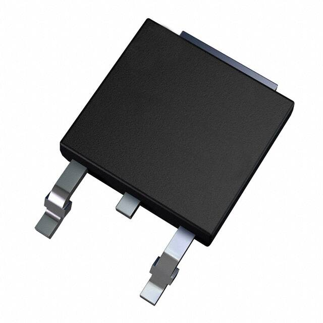
PACKAGE OUTLINE
NJW4185 is mounted to TO-252-3/-5 packages and corresponded to
Low ESR capacitor (MLCC).
The wide input range makes NJW4185 suitable for Automotive
applications, Industrial supplies, Multiple cell battery equipment and
various applications.
FEATURES
Wide Operating Voltage Range
Low Current Consumption
NJW4185DL3
NJW4185DL1
4.0V to 40V
55μA typ. (A version)
48μA typ. (B version)
VO 1.0%
IO(min.)=500mA
2.0V to 15.0V
High Precision Output
Output Current
Output Voltage Range
Correspond to Low ESR capacitor (MLCC)
ON/OFF Function (apply only the A ver.)
Internal Thermal Overload Protection
Internal Over Current Protection
Package Outline
A version: TO-252-5
B version: TO-252-3
PRODUCT CLASSIFICATION
ON/OFF
Function
NJW4185DL3-xxA
A
Yes
NJW4185DL1-xxB
B
xx=Output Voltage ex) 33=3.3V 05=5.0V
Device Name
Version
Package
TO-252-5
TO-252-3
PIN CONFIGURATION
5
4
3
2
1
3
NJW4185DL3-A
Ver.2015-12-01
VOUT
NC
GND
CONTROL
VIN
3 VOUT
2
2 GND
1 VIN
NJW4185DL1-B
-1-
�NJW4185
BLOCK DIAGRAM
・A version
VOUT
VIN
Current
Limit
CONTROL
Bandgap
Reference
Thermal
Protection
GND
・B version
VIN
VOUT
Current
Limit
Bandgap
Reference
Thermal
Protection
GND
OUTPUT VOLTAGE RANK LIST
・A version
Device Name
Output Voltage
NJW4185DL3-33A
3.3V
NJW4185DL3-05A
5.0V
NJW4185DL3-08A
8.0V
NJW4185DL3-15A
15.0V
・B version
Device Name
NJW4185DL1-33B
NJW4185DL1-05B
NJW4185DL1-08B
NJW4185DL1-15B
-2-
Output Voltage
3.3V
5.0V
8.0V
15.0V
Ver.2015-12-01
�NJW4185
ABSOLUTE MAXIMUM RATINGS
PARAMETER
SYNBOL
Input Voltage
VIN
Control Voltage(*1)
VCONT
Output Voltage
VOUT
Power Dissipation
Junction Temperature
Operating Temperature
Storage Temperature
PD
Tj
Topr
Tstg
RATINGS
-0.3 to +45
-0.3 to +45
-0.3 to VIN +17
1190 (*2)
3125 (*3)
-40 to +150
-40 to +125
-40 to +150
(Ta=25 C)
UNIT
V
V
V
mW
C
C
C
(*1): Apply only the A version.
2
(*2): Mounted on glass epoxy board. (76.2 114.3 1.6mm:based on EIA/JDEC standard size, 2Layers, Cu area 100mm )
(*3): Mounted on glass epoxy board. (76.2 114.3 1.6mm:based on EIA/JDEC standard, 4Layers)
(For 4Layers: Applying 74.2 x 74.2mm inner Cu area and thermal via hole to a board based on JEDEC standard JESD51-5)
INPUT VOLTAGE RANGE
VIN=4.0V to 40V
ELECTRICAL CHARACTERISTICS
PARAMETER
SYMBOL
Output Voltage
VO
Quiescent Current
IQ
Quiescent Current
at Control OFF (*4)
Unless otherwise noted, VIN=VO+1V, CIN=1.0μF, CO=2.2μF, Ta=25 C
TEST CONDITION
MIN.
TYP.
MAX.
UNIT
-1.0%
-
+1.0%
A version, IO =0mA, except ICONT
-
55
90
B version, IO =0mA
-
48
83
IQ (OFF)
VCONT =0V
-
-
1
μA
Output Current
IO
VO 0.9
500
-
-
mA
Line Regulation
VO/ VIN
VIN = VO+1V to 40V, IO=30mA
-
-
0.03
%/V
Load Regulation
VO/ IO
IO =0mA to 500mA
-
-
0.006
%/mA
VO=3.3V
-
62
-
VO=5.0V
-
60
-
VO=8.0V
-
55
-
VO=15V
-
50
-
IO =300mA
-
0.27
0.42
V
Ripple Rejection
Dropout Voltage (*5)
RR
VI O
IO =30mA
VIN = VO+1V ,ein=200mVrms,
f=1kHz, IO =10mA
V
μA
dB
Average Temperature
Coefficient of Output Voltage
VO/ Ta
Ta =0 to 85 C, IO =30mA
-
50
-
ppm/ C
Control Current (*4)
ICONT
VCONT=1.6V
-
1
3
μA
VCONT(ON)
1.6
-
-
V
VCONT(OFF)
-
-
0.6
V
Control Voltage
for ON-state (*4)
Control Voltage
for OFF-state (*4)
(*4): Apply only the A version.
(*5): Except Output Voltage Rank less than 3.8V
The above specification is a common specification for all output voltages.
Therefore, it may be different from the individual specification for a specific output voltage.
Ver.2015-12-01
-3-
�NJW4185
THERMAL CHARACTERISTICS
PARAMETER
SYMBOL
Junction-to-Ambient
ja
thermal resistance
Junction-to-Top of package
jt
characterization parameter
VALUE
105 (*6)
40 (*7)
17 (*6)
12 (*7)
UNIT
C/W
C/W
2
(*6): Mounted on glass epoxy board. (76.2 114.3 1.6mm:based on EIA/JDEC standard size, 2Layers, Cu area 100mm )
(*7): Mounted on glass epoxy board. (76.2 114.3 1.6mm:based on EIA/JDEC standard, 4Layers)
(For 4Layers: Applying 74.2 74.2mm inner Cu area and a thermal via hole to a board based on JEDEC standard JESD51-5)
POWER DISSIPATION vs. AMBIENT TEMPERATURE
NJW4185DL1/DL3 PowerDissipation
(Topr=-40~+125°C,Tj=150°C)
3500
Power Dissipation PD(mW)
3000
on 4 layers board
2500
2000
on 2 layers board
1500
1000
500
0
-50
-25
0
25
50
75
100
125
150
Temperature : Ta( C)
-4-
Ver.2015-12-01
�NJW4185
TEST CIRCUIT
・A version
A
IIN
VIN
VIN
1.0μF
ICONT
A
VOUT
NJW4185-A
2.2μF
IOUT V VOUT
(Ceramic)
CONTROL
GND
V VCONT
・B version
A
VIN
IIN
VIN
1.0 F
VOUT
NJW4185-B
2.2 F
IOUT V VOUT
(ceramic)
GND
Ver.2015-12-01
-5-
�NJW4185
TYPICAL APPLICATION
・A version
1. In the case where ON/OFF Control is not required
VIN
VIN
1.0μF
VOUT
NJW4185-A
VOUT
2.2μF
R
CONTROL
GND
Connect control pin to VIN pin
2. In use of ON/OFF CONTROL
VIN
VIN
1.0μF
VOUT
NJW4185-A
VOUT
2.2μF
R
CONTROL
GND
State of control pin:
“H” output is enabled.
“L” or “open” output is disabled.
・B version
VIN
VIN
1.0 F
VOUT
VOUT
2.2 F
NJW4185-B
GND
-6-
Ver.2015-12-01
�NJW4185
*In the case of using a resistance "R" between VIN and control.
If this resistor is inserted, it can reduce the control current when the control voltage is high.
The applied voltage to control pin should set to consider voltage drop through the resistor “R” and the minimum
control voltage for ON-state.
The VCONT (ON) and ICONT have temperature dependence as shown in the "Control Current vs. Temperature" and
"Control Voltage vs. Temperature" characteristics. Therefore, the resistance "R" should be selected to consider the
temperature characteristics.
*Input Capacitor CIN
Input Capacitor CIN is required to prevent oscillation and reduce power supply ripple for applications when high
power supply impedance or a long power supply line.
Therefore, use the recommended CIN value (refer to conditions of ELECTRIC CHARACTERISTIC) or larger and
should connect between GND and VIN as shortest path as possible to avoid the problem.
*Output Capacitor CO
The output capacitor CO will be required for a phase compensation of the internal error amplifier.
The capacitance and the equivalent series resistance (ESR) influence to stable operation of the regulator.
Use of a smaller CO may cause excess an output noise or an oscillation of the regulator due to lack of the
phase compensation.
On the other hand, use of a larger CO reduces an output noise and a ripple output, and also improves an
output transient response when load rapidly changes.
Therefore, use the recommended CO value (refer to conditions of ELECTRIC CHARACTERISTIC) or larger
and should connect between GND and VOUT as shortest path as possible for stable operation.
The recommended capacitance depends on the output voltage rank. Especially, a low voltage regulator requires
larger CO value.
In addition, you should consider varied characteristics of capacitor (a frequency characteristic, a temperature
characteristic, a DC bias characteristic and so on) and unevenness peculiar to a capacitor supplier enough.
When selecting CO, recommend that have withstand voltage margin against an output voltage and superior
temperature characteristic.
*Transient response characteristic of Output Voltage
In general, overshoot or undershoot of output voltage may occur due to the transient response characteristic of an
internal error amplifier.
Especially, low current consumption regulator may have overshoot or undershoot due to slow feedback caused by
current saving design.
Therefore, design validation is important in the following cases:
1. Input voltage or output current change sharply
2. Output capacitors is small
3. Output load is light
4. A regulator starts up with very low dropout voltage operation.
Increasing the value of input and/or output capacitor is a common countermeasure for improving a transient
response characteristic.
A transient response characteristic may vary with operating conditions and external components value.
Please check it with the actual environment.
Ver.2015-12-01
-7-
�NJW4185
*The notes of the evaluation when output pin is shorted to GND
When evaluate short circuit test, the IC may break down because of regenerated energy by the parasitic inductance
included in wiring pattern.
It phenomenon appears conspicuously when an output voltage is higher(Vo=8.0V or more) or connected to
inductive load.
In case of short circuit in actual application, not likely to destruction of the IC because of some of Resistance exist
between load.
If happened above phenomenon by the short circuit test with the actual application, recommend connecting schottky
barrier diode(SBD) between Vo pin and GND or using output capacitors that have ESR more than 2Ω like a tantalum
or aluminum electrolytic capacitor.(see below figure)
(a)In case of insert Schottky barrier diode between output pin - GND
V IN
V IN
V OUT
NJW 4185
V OUT
SBD
GND
(b) In case of using the electrolytic capacitor or insert series resistor
VIN
VIN
VOUT
VOUT
NJW4185
GND
-8-
Connecting resistor(2 or more)in series.
(in case of ESR of COUT is low)
Ver.2015-12-01
�NJW4185
TYPICAL CHARACTERISTICS
NJW4185_5.0V
Output Voltage:VO (V)
Io=0mA
4.9
Io=30mA
@:VIN=4.3V
CIN=1.0μF(Ceramic)
Co=2.2μF(Ceramic)
6
5.1
5
Output Voltage vs Output Current
7
@:Ta=25ºC
CIN=1.0μF(Ceramic)
Co=2.2μF(Ceramic)
5.2
Output Voltage:VO (V)
NJW4185_5.0V
Output Voltage vs Input Voltage
5.3
Io=500mA
4.8
4.7
5
150ºC
4
3
2
0
4.6
4.8
5
5.2
5.4
5.6
Input Voltage:VIN (V)
5.8
6
0
250
500
750
1000
Output Current:Io (mA)
NJW4185(A ver.)_5.0V
450
@:Ta=25ºC
Output is Open
CIN=1.0μF(Ceramic)
Co=2.2μF(Ceramic)
550
Quiescent Current:IQ (μA)
500
Quiescent Current vs Input Voltage
600
@:Ta=25ºC
Output is Open
except ICONT
CIN=1.0μF(Ceramic)
Co=2.2μF(Ceramic)
550
1250
NJW4187(B ver.)_5.0V
Quiescent Current vs Input Voltage
600
Quiescent Current:IQ (μA)
-50ºC
1
4.6
400
350
300
250
200
150
500
450
400
350
300
250
200
150
100
100
50
50
0
0
0
10
20
30
Input Voltage:VIN (V)
0
40
Ground Pin Current vs Output Current
600
40
Output Voltage vs Control Voltage
6
@:Ta=25ºC
VIN=6.0V
CIN=1.0μF(Ceramic)
Co=2.2μF(Ceramic)
@:Ta=25ºC
VIN=6.0V
CIN=1.0μF(Ceramic)
Co=2.2μF(Ceramic)
5
Output Voltage:VO (V)
500
10
20
30
Input Voltage : VIN (V)
NJW4185_5.0V
NJW4185_5.0V
Ground Pin Current:IGND (μA)
25ºC
400
300
200
100
Rc=100kΩ
4
3
Rc=0Ω
2
1
0
0
0
Ver.2015-12-01
100
200
300
400
Output Current:Io (mA)
500
0
0.5
1
1.5
Control Voltage:VCONT (V)
2
-9-
�NJW4185
NJW4185_5.0V
Load Regulation vs Output Current
0
@:Ta=25ºC
VIN=6.0V
CIN=1.0μF(Ceramic)
Co=2.2μF(Ceramic)
70
60
Load Regulation :ΔVo/ΔIo (mV)
Control Current:ICONT (μA)
80
NJW4185_5.0V
Control Current vs Control Voltage
50
Rc=0Ω
40
30
Rc=100kΩ
20
10
0
-20
-40
-60
-80
-100
-120
@:Ta=25ºC
VIN=6.0V
CIN=1.0μF(Ceramic)
Co=2.2μF(Ceramic)
-140
-160
0
10
20
30
Control Voltage:VCONT (V)
40
0
100
200
300
400
Output Current:Io (mA)
NJW4185_5.0V
NJW4185_5.0V
Peak Output Current vs Input Voltage
Dropout Voltage:ΔVI-O (V)
800
600
400
@:Ta=25ºC
VO=4.5V
CIN=1.0μF(Ceramic)
Co=2.2μF(Ceramic)
200
0
6
100
Ripple Rejection Ratio:RR (dB)
@:Ta=25ºC
CIN=1.0μF(Ceramic)
Co=2.2μF(Ceramic)
0.7
1000
10
34
100
200
300
400
Output Current:Io (mA)
NJW4185_5.0V
100
40
30
@Ta=25ºC
VIN=6.0V
Cin=1.0μF(Ceramic)
Co=2.2μF(Ceramic)
ein=200mVrms
10
0
Ripple Rejection Ratio vs Output Current
Io=100mA
0
0.2
NJW4185_5.0V
Io=30mA
10
0.3
Ripple Rejection Ratio vs Frequency
70
20
0.4
38
Io=0mA
50
0.5
0
14 18 22 26 30
Input Voltage:VIN (V)
80
60
0.6
0.1
Io=10mA
90
- 10 -
Dropout Voltage vs Output Current
0.8
Ripple Rejection Ratio:RR (dB)
Peak Output Current:IOPEAK (mA)
1200
100
500
Io=500mA
1k
Frequency:f
10k
(Hz)
100k
500
90
80
70
f=1kHz
60
50
40
f=10kHz
30
20
10
@Ta=25ºC
VIN=6.0V
Cin=1.0μF(Ceramic)
Co=2.2μF(Ceramic)
ein=200mVrms
0
0.001
0.01
0.1
1
10
100
Output Current:Io (mA)
1000
Ver.2015-12-01
�NJW4185
NJW4185_5.0V
100
10
Output Voltage vs Temperature
5.3
@VIN=6.0V
Cin=1.0μF(Ceramic)
Co=2.2μF(Ceramic)
1
Stable Region
0.1
0.01
Io=0
@:VIN=6.0V
CIN=1.0μF(Ceramic)
Co=2.2μF(Ceramic)
5.2
Output Voltage:VO (V)
Equivalent Series Resistance:ESR (Ω)
NJW4185_5.0V
Equivalent Series Resistance vs Output Current
Io=30mA
Io=500mA
5.1
5
4.9
4.8
4.7
4.6
0.001
0.001
4.5
0.01
0.1
1
10
100
Output Current:Io (mA)
-50
1000
0
NJW4185_5.0V
Control Current:ICONT (μA)
Control Voltage:VCONT (V)
1.2
1
0.8
0.6
0.4
0.2
@:VCONT=1.6V
CIN=1.0μF(Ceramic)
Co=2.2μF(Ceramic)
3.5
3
2.5
2
1.5
1
0.5
0
0
-50
0
50
Temperature:
100
150
-50
150
Short Cuircuit Current vs Temperature
1000
VIN=6V
VIN=40V
900
600
300
Short Circuit Current:ISC (mA)
Peak Output Current:IOPEAK (mA)
@:VO=4.5V
CIN=1.0μF(Ceramic)
Co=2.2μF(Ceramic)
50
100
Temperature:(ºC)
NJW4185_5.0V
Peak Output Current vs Temperature
1500
0
(ºC)
NJW4185_5.0V
1200
150
Control Current vs Temperature
4
@:VIN=6.0V
CIN=1.0μF(Ceramic)
Co=2.2μF(Ceramic)
1.4
100
(ºC)
NJW4185_5.0V
Control Voltage vs Temperature
1.6
50
Temperature:
@:VO=0V
CIN=1.0μF(Ceramic)
Co=2.2μF(Ceramic)
900
800
VIN=6V
VIN=40V
700
600
500
400
300
200
100
0
0
-50
Ver.2015-12-01
0
50
100
Temperature:(ºC)
150
-50
0
50
100
Temperature : (ºC)
150
- 11 -
�NJW4185
NJW4185_5.0V
Load Regulation vs Temperature
0.05
@:VIN=6.0-40V
Io=30mA
CIN=1.0μF(Ceramic)
Co=2.2μF(Ceramic)
0.025
Load Regulation:ΔVo/ΔIo (%/mA)
Line Regulation: ΔVo/ΔVIN (%/V)
0.05
NJW4185_5.0V
Line Regulation vs Temperature
0
-0.025
-0.05
@:VIN=6.0V
Io=0-500mA
CIN=1.0μF(Ceramic)
Co=2.2μF(Ceramic)
0.025
0
-0.025
-0.05
-50
0
50
100
Temperature: (ºC)
150
-50
Dropout Voltage :VIO (V)
Output Voltage:VO (V)
5
4
3
Io=0mA
Io=30mA
Io=500mA
150
@:CIN=1.0μF(Ceramic)
Co=2.2μF(Ceramic)
0.8
Io=100mA
Io=300mA
Io=500mA
0.7
0.6
0.5
0.4
0.3
0.2
@:VIN=6.0V
CIN=1.0μF(Ceramic)
Co=2.2μF(Ceramic)
1
100
(ºC)
Dropout Voltage vs Temperature
1
0.9
2
50
Temperature:
NJW4185_5.0V
NJW4185_5.0V
Output Voltage vs Temperature
6
0
0.1
0
0
-50
50
Temperature:
150
-50
(ºC)
0
50
100
Temperature : (ºC)
150
NJW4185(A ver.)_5.0V
Quiescent Current vs Temperature
100
Quiescent Current:IQ (μA)
90
@:VIN=6.0V
Output is Open
except ICONT
CIN=1.0μF(Ceramic)
Co=2.2μF(Ceramic)
80
70
60
50
40
30
20
10
0
-50
- 12 -
0
50
Temperature:
100
150
(ºC)
Ver.2015-12-01
�NJW4185
NJW4185_5.0V
NJW4185_5.0V
Input Transient Response
Load Transient Response
7
5
@:Ta=25 C
VIN=6.0-7.0V
Io=30mA
CIN=1.0μF(Ceramic)
Co=2.2μF(Ceramic)
4
3
5.1
2
5.0
Output Voltage
1
Output Voltage:Vo (V)
6
Output Voltage:VO (V)
Input Voltage
Input Voltage:VIN (V)
@:Ta=25 C
VIN=6.0V
Io=0-100mA
CIN=1.0μF(Ceramic)
Co=2.2μF(Ceramic)
200
100
Output Current
0
5.1
5.0
Output Voltage
4.9
Output Current :Io (mA)
300
4.9
0
40
80
120
160
200
0
Time:t (μs)
200
600
800
1000
Time:t (ms)
NJW4185(A ver.)_5.0V
NJW4185(A ver.)_5.0V
ON/OFF Transient Response without Load
ON/OFF Transient Response
12
12
10
8
6
Output Voltage
4
2
5
0
0
Control Voltage:VCONT (V)
@:Ta=25 C
VIN=6.0V
Io=0mA
CIN=1.0μF(Ceramic)
Co=2.2μF(Ceramic)
Output Voltage:VO (V)
Control Voltage:VCONT (V)
400
@:Ta=25 C
VIN=6.0V
Io=30mA
CIN=1.0μF(Ceramic)
Co=2.2μF(Ceramic)
Output Voltage
10
8
6
4
2
5
0
Output Voltage:VO (V)
0
0
Control Voltage
0
20
40
Control Voltage
60
Time:t (s)
80
100
0
4
8
12
16
20
Time:t (ms)
[CAUTION]
The specifications on this databook are only
given for information , without any guarantee
as regards either mistakes or omissions. The
application circuits in this databook are
described only to show representative usages
of the product and not intended for the
guarantee or permission of any right including the
industrial rights.
Ver.2015-12-01
- 13 -
�
很抱歉,暂时无法提供与“NJW4185DL1-05B-TE1”相匹配的价格&库存,您可以联系我们找货
免费人工找货