Advanced Science And Novel Technology Company, Inc.
2790 Skypark Drive Suite 112, Torrance, CA 90505
Offices: 310-530-9400 / Fax: 310-530-9402
www.adsantec.com
ASNT5144-KHC
8-35GHz Automatic Frequency Doubler
High-speed frequency doubler with automatic output duty cycle correction.
Output duty cycle always 50% with internal feedback turned on.
Manual output duty cycle control available.
Exhibits low jitter and limited temperature variation over industrial temperature range.
Ideal for high speed proof-of-concept prototyping.
Fully differential CML input interfaces.
Fully differential CML output interface with 600mV single-ended swing.
Single +3.3V or -3.3V power supply.
Power consumption: 660mW.
Fabricated in SiGe for high performance, yield, and reliability.
Custom CQFN 24-pin package
Rev.1.0.2
1
April 2021
�Advanced Science And Novel Technology Company, Inc.
2790 Skypark Drive Suite 112, Torrance, CA 90505
Offices: 310-530-9400 / Fax: 310-530-9402
www.adsantec.com
DESCRIPTION
Fig. 1. Functional Block Diagram
The temperature stable ASNT5144-KHC SiGe IC provides broadband frequency multiplication, and is
intended for use in high-speed measurement / test equipment. The IC shown in Fig. 1 can receive a highspeed clock input signal ip/in, and deliver a high-speed double-frequency clock output signal outp/outn.
There are two duty cycle correction feedback loops. The first loop adjusts the duty cycle of the input
signal, and the second loop controls the final output signal duty cycle. Activation of the loops is
controlled via the onfb control port as shown in Table 1.
Table 1. Feedback Loops Activation by onfb
fbon
Input FB loop Output FB loop
off
off
vee
off
on
vcc
not connected (nc)
on
on
When both feedback loops are activated, the output clock’s duty cycle is automatically kept at about 50%.
To ensure correct operation of the feedback block within a wide range of frequencies, the optional control
port crl can be set to vee/vcc/nc according to Table 2. The duty cycle may also be adjusted manually via
tuning ports icntp/icntn when feedback is turned off.
Table 2. Frequency Ranges at crl settings
crl
Frequency Range (GHz)
4.3 - 12.9
vee
6.6 - 19.7
vcc
not connected (nc)
13 - 38.9
The part’s I/O’s support the CML logic interface with on chip 50Ohm termination to vcc, and may be
used differentially, AC/DC coupled, single-ended, or in any combination (also see POWER SUPPLY
CONFIGURATION). In the DC-coupling mode, the input signal’s common mode voltage should comply
with the specifications shown in ELECTRICAL CHARACTERISTICS. In the AC-coupling mode, the
input termination provides the required common mode voltage automatically. The differential DC
signaling mode is recommended for optimal performance.
Rev.1.0.2
2
April 2021
�Advanced Science And Novel Technology Company, Inc.
2790 Skypark Drive Suite 112, Torrance, CA 90505
Offices: 310-530-9400 / Fax: 310-530-9402
www.adsantec.com
POWER SUPPLY CONFIGURATION
The part can operate with either a negative supply (vcc = 0.0V = ground and vee = −3.3V), or a positive
supply (vcc = +3.3V and vee = 0.0V = ground). In case of the positive supply, all I/Os need AC
termination when connected to any devices with 50Ohm termination to ground. Different PCB layouts
will be needed for each different power supply combination.
All the characteristics detailed below assume vcc = 0.0V and vee = -3.3V.
ABSOLUTE MAXIMUM RATINGS
Caution: Exceeding the absolute maximum ratings shown in Table 3 may cause damage to this product
and/or lead to reduced reliability. Functional performance is specified over the recommended operating
conditions for power supply and temperature only. AC and DC device characteristics at or beyond the
absolute maximum ratings are not assumed or implied. All min and max voltage limits are referenced to
ground.
Table 3. Absolute Maximum Ratings.
Parameter
Supply Voltage (vee)
Supply current
RF Input Voltage Swing (SE)
Case Temperature
Storage Temperature
Operational Humidity
Storage Humidity
Min
-40
10
10
Max
-3.6
200
1.0
+90
+100
98
98
Units
V
mA
V
ºC
ºC
%
%
TERMINAL FUNCTIONS
TERMINAL
Name No.
Type
ip
in
outp
outn
onfb
crl
icntp
icntn
Name
vcc
vee
Rev.1.0.2
DESCRIPTION
High-Speed I/Os
21 CML input Differential clock inputs with internal SE 50Ohm termination
to vcc.
23
11 CML output Differential clock outputs with internal SE 50Ohm termination
to vcc. Require external SE 50Ohm termination to vcc.
9
15 3.3V CMOS Digital Control Signal with 6.6KOhm termination to vee
17 3.3V CMOS 3-State Digital Control Signal with 4.6KOhm termination to
vee and 6.6KOhm termination to vcc
3 CML input Differential tuning ports with internal 100Ohm termination to
vcc.
5
Supply and Termination Voltages
Description
Pin Number
Positive power supply. (+3.3V or 0)
2, 4, 6, 8, 10, 12, 14, 16, 18, 20, 22, 24
Negative power supply. (0V or -3.3V)
3
1, 7, 13, 19
April 2021
�Advanced Science And Novel Technology Company, Inc.
2790 Skypark Drive Suite 112, Torrance, CA 90505
Offices: 310-530-9400 / Fax: 310-530-9402
www.adsantec.com
ELECTRICAL CHARACTERISTICS
PARAMETER
vee
vcc
Ivee
Power consumption
Junction temperature
Frequency
Swing
CM Voltage Level
Frequency
Logic “1” level
Logic “0” level
Rise/Fall times
Output Jitter
Duty cycle
onfb
crl
Bandwidth
Swing
CM Voltage Level
Rev.1.0.2
MIN
TYP
MAX UNIT
COMMENTS
General Parameters
-3.1
-3.3
-3.5
V
±6%
0.0
V
External ground
200
mA
660
mW
-40
25
125
°C
HS Input Clock (ip/in)
4
17.5
GHz
0.05
1.0
V
Differential or SE, p-p
vcc-0.8
vcc
V
Must match for both inputs
HS Output Clock (outp/outn)
8
35
GHz
V
vcc
vcc-0.6
V
With external 50Ohm DC termination
6
8
10
ps
20%-80%
1
ps
Peak-to-peak
50
%
For clock signal with feedback on
CMOS Control Ports (onfb, crl)
0
3.3
V
See Table 1
0
nc
3.3
V
See Table 2
Tuning Ports (icntp/icntn)
DC
100
MHz
vcc-0.4
V
Differential
vcc-0.4
vcc
V
Must match for both inputs
4
April 2021
�Advanced Science And Novel Technology Company, Inc.
2790 Skypark Drive Suite 112, Torrance, CA 90505
Offices: 310-530-9400 / Fax: 310-530-9402
www.adsantec.com
PACKAGE INFORMATION
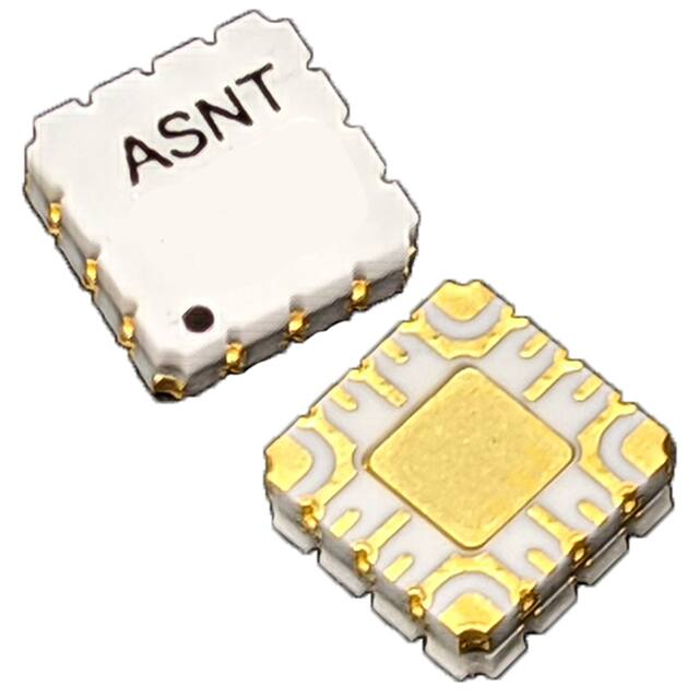
The chip die is housed in a custom 24-pin CQFN package shown in Error! Reference source not found..
The package provides a center heat slug located on its back side to be used for heat dissipation.
ADSANTEC recommends for this section to be soldered to the vcc plain, which is ground for a negative
supply, or power for a positive supply.
Fig. 2. CQFN 24-Pin Package Drawing (All Dimensions in mm)
Rev.1.0.2
5
April 2021
�Advanced Science And Novel Technology Company, Inc.
2790 Skypark Drive Suite 112, Torrance, CA 90505
Offices: 310-530-9400 / Fax: 310-530-9402
www.adsantec.com
The part’s identification label is ASNT5144-KHC. The first 8 characters of the name before the dash
identify the bare die including general circuit family, fabrication technology, specific circuit type, and part
version while the 3 characters after the dash represent the package’s manufacturer, type, and pin out
count.
This device complies with Commission Delegated Directive (EU) 2015/863 of 4 June 2015 amending
Annex II to Directive 2011/65/EU of the European Parliament and of the Council as regards the list of
restricted substances (Text with EEA relevance) on the restriction of the use of certain hazardous
substances in electrical and electronics equipment (RoHS Directive) in accordance with the definitions set
forth in the directives for all ten substances.
REVISION HISTORY
Revision
1.0.2
Rev.1.0.2
Date
04-2021
Changes
First release
6
April 2021
�